Abstract
Perovskite-based metal oxide phototransistors have emerged as promising photodetection devices owing to the superior optoelectronic properties of perovskite materials and the high carrier mobility of metal oxides. However, high dark current has been one major problem for this type of device. Here, we studied the dark current behaviors of phototransistors fabricated based on the Indium Gallium Zinc Oxide (IGZO) channel and different perovskite materials. We found that depositing organic–inorganic hybrid perovskites materials (MAPbI3/FAPbI3/FA0.2MA0.8PbI3) on top of IGZO transistor can increase dark current from ~10−6 mA to 1~10 mA. By contrast, we observed depositing an inorganic perovskite material, CsPbI3, incorporated with PCBM additive can suppress the dark current down to ~10−6 mA. Our study of ion migration reveals that ion migration is pronounced in organic–inorganic perovskite films but is suppressed in CsPbI3, particularly in CsPbI3 mixed with PCBM additive. This study shows that ion migration suppression by the exclusion of organic halide and the incorporation of PCBM additive can benefit low dark current in perovskite phototransistors.
1. Introduction
Phototransistors have obtained an increasing amount of research attention owing to their advantages of compatibility with transistor circuit manufacture and photodetection gain effect [1,2,3,4,5,6]. Over recent years, perovskite semiconductors have been developed remarkably, showing their high optoelectronic performance, such as quantum efficiency of over 90% and carrier lifetime of over 1 μs [7,8,9,10]. Therefore, developing phototransistors using perovskite light absorbers has been promoted as a promising solution for high-performance photodetection technology and has gained more research attention [11,12,13,14,15,16]. Moreover, the phototransistor requires a channel layer of high carrier mobility, a wide band gap for modulating a high on/off ratio for high detectivity, and good transparency and chemical robustness for depositing the perovskite layer through solution reaction. These requirements lead to the use of metal oxide semiconductors, which are known for mobility over 40 cm2V−1s−1 [17,18,19,20], large band gap over 3.5 eV, which produces ideal transparency to visible light, and reliable chemical stability and durability [21,22,23,24]. Therefore, developing phototransistors based on perovskite as the light absorber and metal oxide as the channel layer is an effective solution for pursuing high-detectivity photodetection.
In these reports of phototransistors based on perovskites and metal oxides [25,26,27,28], there are observations of high dark current after depositing perovskites on top of a metal oxide channel, leading to very poor photo detectivity. This is a major problem hindering the development of perovskite phototransistors. Therefore, it is important to understand the interplay between material property and the high dark current behavior in order to obtain solutions. We investigated the dark current behavior on phototransistors based on a wide range of perovskite materials, MAPbI3/FAPbI3/FA0.2MA0.8PbI3/CsPbI3 (MA and FA denote CH3NH3 and CH4N2). Our results show that dark current rise is relevant to ion migrations that are pronounced in perovskites of organic halides and are relatively suppressed in fully inorganic perovskites, CsPbI3. Moreover, we found that by using PCBM additive into the CsPbI3 film, the ion migration is further reduced, and correspondingly, the CsPbI3/PCBM phototransistor exhibits a dark current down below 10−6 mA. Our study provides an in-depth understanding of the dark current behavior of perovskite phototransistors and an effective device solution to obtain a low dark current for photodetection operation.
2. Materials and Methods
As shown in Figure 1, a Si/SiO2 wafer was cut into 15 mm × 15 mm substrates using a laser fragment system, with the highly doped silicon layer and the SiO2 layer (300 nm) serving as the gate electrode and the dielectric layer, respectively. First, the substrates were cleaned with an ultrasonic bath in Decon 90 (with deionized water), deionized water, acetone, and isopropanol for 10 min each. Then, the substrates were dried using a nitrogen gun and treated with oxygen plasma for 5 min. After that, the substrates were again cleaned with isopropanol for 5 min. IGZO material was sputtered onto the substrate through a shadow mask under a high vacuum (8 × 10⁻⁴ Pa) as the active layer. On this basis, LOR 5B and S1813 photoresist were spin-coated at a speed of 6000 rpm, pre-baked for 5 min and 2 min, respectively, and then developed after photolithography to pattern the source and drain electrodes, followed by the deposition of gold onto the substrate to a thickness of 30 nm at a rate of 1~2 Å/s through thermal evaporation. By weighing 1.5 mmol of the perovskite precursor, a 2 mL solution of 0.75 mol/L perovskite was prepared using N,N-Dimethylformamide (DMF): Dimethyl sulfoxide (DMSO) = 9:1(V:V) as the solvent. Then, 80 μL of the perovskite solution was dropped onto the substrate surface, followed by an immediate spin-coating at 5000 rpm for 15 s. Afterward, the sample was annealed at 100 °C for 10 min in a nitrogen atmosphere.
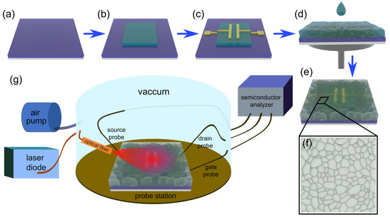
Figure 1.
(a)–(e) Schematic diagram of the device fabrication process; (a) cleaning the substrate; (b) sputtering IGZO; (c) depositing the electrode after lithography; (d) spinning perovskite solution; (e) annealing to form a film; (f) schematic diagram of the perovskite film; (g) electrical measurement schematic.
Electrical measurements were conducted at room temperature in a vacuum probe station, as shown in Figure 1g. All transfer and output characteristics were measured using a Keithley 2636B semiconductor analyzer and kickstart-2 software. The ion migration in the device is reflected by the timing change of the source-drain current at a fixed bias voltage. We measured the current changing over a 30-s period under a bias of VD = 5 V and VG = 5 V. Illumination was provided by a 650 nm wavelength laser diode with different light intensities. The light source illuminates the equipment through optical fibers in the probe station while the equipment is in a vacuum state inside the probe station. The scanning electron microscopy (SEM) used in the experiment is Zeiss Sigma 300, with secondary electronic resolution ≤1.0 nm@15 kV, ≤1.6 nm@1 kV, electron beam acceleration voltage 0.02 kV ~ 30 kV, step by 10 V, and continuous adjustable.
3. Results and Discussion
Figure 2 shows the transfer curve characteristics and the output characteristics curve of the IGZO transistor, both of which were measured under dark conditions. From the transfer curve (Figure 2a), we obtain high carrier mobility with the linear region one of 28.1 cm2V−1s−1 and saturation region one of 41.6 cm2V−1s−1, respectively. In addition, a small threshold voltage (VTH = −1 V) is extracted from the transfer curve, indicating the fabricated IGZO transistors are of small contact resistance that is consistent with the output characteristics (Figure 2b). This result confirms that our fabricated IGZO transistor is of standard high performance.
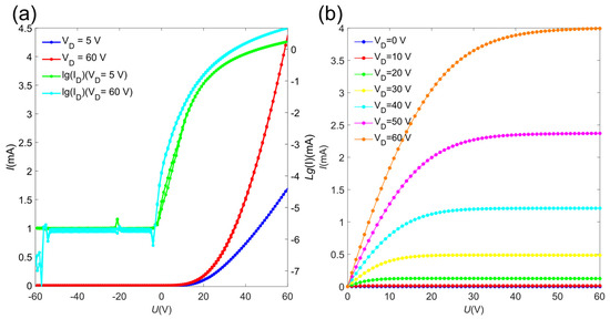
Figure 2.
IGZO device electrical performance, (a) transfer curve characteristic data, (b)output characteristic data.
On top of the surface of the IGZO transistor, we spin-coated perovskite layers to fabricate phototransistors. Here, we studied eight types of phototransistors based on four perovskite compositions and PCBM additive added to each composition. The eight devices are phototransistors of CsPbI3, CsPbI3-PCBM, FA0.2MA0.8PbI3, FA0.2MA0.8PbI3-PCBM, FAPbI3, FAPbI3-PCBM, MAPbI3, and MAPbI3-PCBM, respectively. We studied the dark current of these devices, and the transfer curve characteristics of all devices measured under dark conditions are shown in Figure 3. The red curve and the blue curve in Figure 3 represent the transfer characteristic curves measured of perovskite phototransistors without PCBM and perovskite phototransistors with PCBM, respectively.
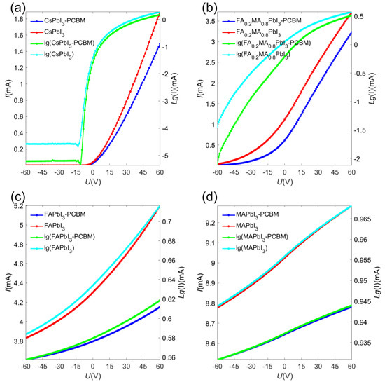
Figure 3.
Linear region transfer curve characteristic data measured under dark conditions (a) CsPbI3−PCBM and CsPbI3; (b) FA0.2MA0.8PbI3−PCBM and FA0.2MA0.8PbI3; (c) FAPbI3−PCBM and FAPbI3; (d) MAPbI3−PCBM and MAPbI3.
For comparison, we examine the dark current at the gate voltage where the minimal dark current is obtained for all devices, which is shown in Table 1.

Table 1.
Dark current and γ of phototransistors with different materials.
From the results, we conclude the following three trends. Firstly, the application of organic–inorganic hybrid perovskite (FA0.2MA0.8PbI3, FAPbI3, MAPbI3) on the top of IGZO surface can largely increase the dark current by several orders of magnitude (compared with the IGZO transistor without depositing perovskite layer), while the deposition of inorganic perovskite (CsPbI3) can still allow low dark current. Secondly, the application of PCBM additive into all perovskites can suppress the enlargement of dark current in their perovskite phototransistors, but not to a satisfactory level. Thirdly, the minimal dark current is observed in the CsPbI3-PCBM phototransistors.
We presume that the underlying mechanism is associated with the ion migration effect, which has been reported as one source of inducing extra current during the operation of perovskite optoelectronic devices [27]. Therefore, we then study the ion migration behavior within the perovskite layer of all devices. Figure 4 shows the results of ion migration measurement. We probe the ion migration effect by inspecting the current evolution while applying an external bias across the source-drain electrodes because ion migration towards electrodes can increase the channel current by lowering the injection barrier and enhancing the tunneling effect [14], as illustrated in Figure 4e,f. For comparison, we extract the proportion of maximum current (Imax, the maximum current reached during the external bias period) over initial current (Iinitial, the current at t = 0 s when external bias starts), as γ = Imax/Iinitial. We obtain γ of all phototransistors with different materials and list them in Table 1. It shows that ion migration is pronounced in organic–inorganic hybrid perovskite samples but is relatively small in the CsPbI3 sample and particularly in the CsPbI3-PCBM sample.
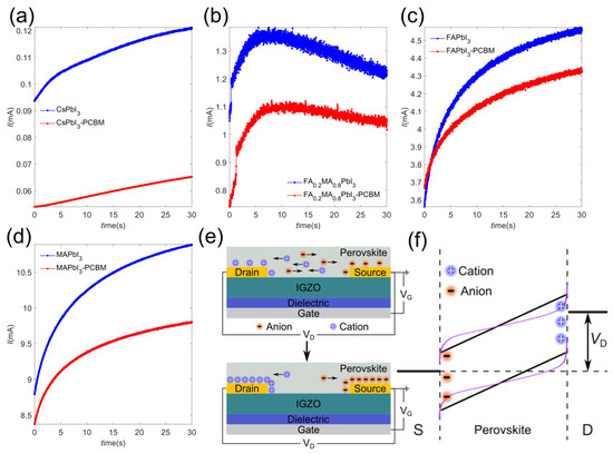
Figure 4.
The graph of the source-drain current changing within 30 s under a bias of VD = 5 V and VG = 5 V; (a) CsPbI3−PCBM and CsPbI3; (b) FA0.2MA0.8PbI3−PCBM and FA0.2MA0.8PbI3; (c) FAPbI3−PCBM and FAPbI3; (d) MAPbI3−PCBM and MAPbI3; (e) Schematic diagram of ion migration in perovskites; (f) Changes in energy levels caused by ion migration in perovskites.
To gain a deep insight, we inspected the microstructural characteristics of perovskite films by SEM. The SEM images shown in Figure 5 reveal the crystalline nature of perovskite grains is well preserved after the incorporation of the PCBM additive, suggesting that the PCBM additive might only be resident in the grain boundaries. This suggests that PCBM may suppress the ion transport between adjacent gains or lower the rate of ion migration, thus suppressing ion migration throughout the film. We presume the reason why CsPbI3-PCBM outperforms the candidates of organic–inorganic hybrid perovskite and PCBM additive are that the organic halide in the hybrid perovskites might have a reaction with the IGZO channel, as reported elsewhere [28], while CsPbI3 is of no organic halide.
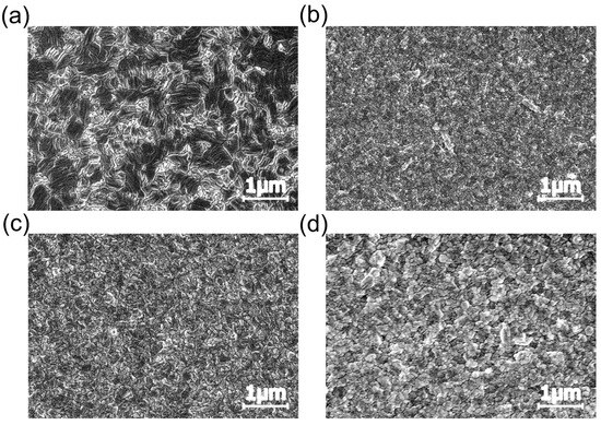
Figure 5.
SEM images of different perovskite material films; (a) CsPbI3-PCBM; (b) FA0.2MA0.8PbI3-PCBM; (c) FAPbI3-PCBM; (d) MAPbI3-PCBM.
The above concludes that the dark current and ion migration are effectively reduced in the CsPbI3-PCBM system. Therefore, we then probe the photodetection performance of the CsPbI3-PCBM phototransistor. We measured both the static photoresponse performance and the dynamic photoresponse performance, and the results are given in Figure 6. The static photoresponse performance is probed by measuring the transfer curves under light intensity (50~100 mW/cm2), as shown in Figure 6a. To evaluate the device’s photodetection performance, we extract detectivity (D) and photoresponsivity (R) by the following equation:
In the formula, represents the photocurrent, P is the incident light power, q is the elementary charge, and represents the dark current. Figure 6c,d shows the obtained data of D and R in dependence of VG extracted from the transfer curves under different light intensities. The peak of detectivity is obtained at around VG = −13 V, where the minimal dark current is reached. The maximum values of D and R are 3.00 × 10¹² Jones and 47.16 A/W, respectively. We further probe the dynamic photoresponse performance of CsPbI3-PCBM phototransistors by measuring the device current of under light signal switching on and off (5 s on and 5 s off), and the results are shown in the inset of Figure 6b. It shows that photocurrent can respond instantly to changes in light intensity.
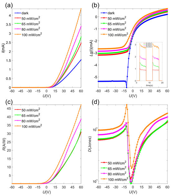
Figure 6.
Photoresponse characteristics of CsPbI3−PCBM: Transfer curve characteristic under different light intensity conditions (a) linear plot and (b) logarithmic plot, the inset in (b) is the result of light switching response; (c) photoresponse responsivity; (d) photoresponse detectivity.
4. Conclusions
In this work, we found that the high dark current in perovskite phototransistors is owed to the ion migration within the perovskite layer, and this is particularly pronounced in organic–inorganic hybrid perovskites. In addition, we found using an inorganic perovskite CsPbI3 film incorporated with PCBM additive is an effective solution to reduce ion migration and achieve a low dark current for reliable photodetection performance. The insights and the device solution in our work would be beneficial for pursuing high-performance perovskite phototransistors.
Author Contributions
C.H. and Y.Y. conducted the experiment. Y.L. and S.J. conducted investigation. L.Y. and R.L. analyzed the data. X.S. established the interpretation and supervised the work. All authors wrote and revised the manuscript. All authors have read and agreed to the published version of the manuscript.
Funding
The authors acknowledged the financial support from the Hundred-talents Program of Zhejiang University (No. 1942221R3/005).
Institutional Review Board Statement
Not applicable.
Informed Consent Statement
Not applicable.
Data Availability Statement
The raw data can be accessed upon request from the authors.
Conflicts of Interest
The authors declare no conflict of interest.
References
- Wang, Y.; Zhang, Y.; Pang, T.; Sun, K.; Hu, Z.; Zhu, Y.; Jia, R. Organolead Halide Perovskite-Based Metal-Oxide-Semiconductor Structure Photodetectors Achieving Ultrahigh Detectivity. Sol. Energy 2019, 183, 226–233. [Google Scholar] [CrossRef]
- Erodici, M.P.; Pierone, P.J.; Hartono, N.T.P.; Hidalgo, J.; Lai, B.; Buonassisi, T.; Correa-Baena, J.-P.; Sher, M.-J. Enhanced Charge Carrier Lifetime and Mobility as a Result of Rb and Cs Incorporation in Hybrid Perovskite. Appl. Phys. Lett. 2021, 118, 063901. [Google Scholar] [CrossRef]
- Kang, C.H.; Dursun, I.; Liu, G.; Sinatra, L.; Sun, X.; Kong, M.; Pan, J.; Maity, P.; Ooi, E.-N.; Ng, T.K.; et al. High-Speed Colour-Converting Photodetector with All-Inorganic CsPbBr3 Perovskite Nanocrystals for Ultraviolet Light Communication. Light Sci. Appl. 2019, 8, 94. [Google Scholar] [CrossRef] [PubMed]
- Chen, T.; Zhan, S.; Li, B.; Hou, B.; Zhou, H. A Low-Toxic Colloidal Quantum Dots Sensitized IGZO Phototransistor Array for Neuromorphic Vision Sensors. Adv. Opt. Mater. 2024, 2302451. [Google Scholar] [CrossRef]
- Xie, C.; You, P.; Liu, Z.; Li, L.; Yan, F. Ultrasensitive Broadband Phototransistors Based on Perovskite/Organic-Semiconductor Vertical Heterojunctions. Light Sci. Appl. 2017, 6, e17023. [Google Scholar] [CrossRef] [PubMed]
- Jiang, S.; Yang, L.; Huang, C.; Chen, Q.; Zeng, W.; She, X. Understanding Illumination Effect on Saturation Behavior of Thin Film Transistor. Photonics 2023, 10, 309. [Google Scholar] [CrossRef]
- Guo, J.; Wang, B.; Lu, D.; Wang, T.; Liu, T.; Wang, R.; Dong, X.; Zhou, T.; Zheng, N.; Fu, Q.; et al. Ultralong Carrier Lifetime Exceeding 20 ms in Lead Halide Perovskite Film Enable Efficient Solar Cells. Adv. Mater. 2023, 35, 2212126. [Google Scholar] [CrossRef] [PubMed]
- Wehrenfennig, C.; Eperon, G.E.; Johnston, M.B.; Snaith, H.J.; Herz, L.M. High Charge Carrier Mobilities and Lifetimes in Organolead Trihalide Perovskites. Adv. Mater. 2014, 26, 1584–1589. [Google Scholar] [CrossRef] [PubMed]
- She, X.-J.; Chen, C.; Divitini, G.; Zhao, B.; Li, Y.; Wang, J.; Orri, J.F.; Cui, L.; Xu, W.; Peng, J.; et al. A Solvent-Based Surface Cleaning and Passivation Technique for Suppressing Ionic Defects in High-Mobility Perovskite Field-Effect Transistors. Nat. Electron. 2020, 3, 694–703. [Google Scholar] [CrossRef]
- Xing, G.; Mathews, N.; Sun, S.; Lim, S.S.; Lam, Y.M.; Grätzel, M.; Mhaisalkar, S.; Sum, T.C. Long-Range Balanced Electron- and Hole-Transport Lengths in Organic-Inorganic CH3NH3PbI3. Science 2013, 342, 344–347. [Google Scholar] [CrossRef] [PubMed]
- Ran, P.; Chen, X.; Chen, Z.; Su, Y.; Hui, J.; Yang, L.; Liu, T.; Tang, X.; Zhu, H.; She, X.; et al. Metal Halide CsCu2I3 Flexible Scintillator with High Photodiode Spectral Compatibility for X-ray Cone Beam Computed Tomography (CBCT) Imaging. Laser Photonics Rev. 2024, 18, 2300743. [Google Scholar] [CrossRef]
- Cho, K.; Yamada, T.; Tahara, H.; Tadano, T.; Suzuura, H.; Saruyama, M.; Sato, R.; Teranishi, T.; Kanemitsu, Y. Luminescence Fine Structures in Single Lead Halide Perovskite Nanocrystals: Size Dependence of the Exciton–Phonon Coupling. Nano Lett. 2021, 21, 7206–7212. [Google Scholar] [CrossRef] [PubMed]
- Stoumpos, C.C.; Malliakas, C.D.; Kanatzidis, M.G. Semiconducting Tin and Lead Iodide Perovskites with Organic Cations: Phase Transitions, High Mobilities, and Near-Infrared Photoluminescent Properties. Inorg. Chem. 2013, 52, 9019–9038. [Google Scholar] [CrossRef] [PubMed]
- Yang, L.; Huang, C.; Chen, Q.; Zeng, W.; She, X.-J. A Vertical Phototransistor of Perovskite/Polymer Nano Heterojunction for Minimizing Ionic Defects. IEEE Electron Device Lett. 2023, 44, 1488–1491. [Google Scholar] [CrossRef]
- Gao, L.; Zeng, K.; Guo, J.; Ge, C.; Du, J.; Zhao, Y.; Chen, C.; Deng, H.; He, Y.; Song, H.; et al. Passivated Single-Crystalline CH3NH3PbI3 Nanowire Photodetector with High Detectivity and Polarization Sensitivity. Nano Lett. 2016, 16, 7446–7454. [Google Scholar] [CrossRef] [PubMed]
- Zhang, F.; Yang, B.; Mao, X.; Yang, R.; Jiang, L.; Li, Y.; Xiong, J.; Yang, Y.; He, R.; Deng, W.; et al. Perovskite CH3NH3PbI3-xBrx Single Crystals with Charge-Carrier Lifetimes Exceeding 260 Μs. ACS Appl. Mater. Interfaces 2017, 9, 14827–14832. [Google Scholar] [CrossRef] [PubMed]
- Sheng, J.; Hong, T.; Lee, H.-M.; Kim, K.; Sasase, M.; Kim, J.; Hosono, H.; Park, J.-S. Amorphous IGZO TFT with High Mobility of ∼70 cm2/(V·s) via Vertical Dimension Control Using PEALD. ACS Appl. Mater. Interfaces 2019, 11, 40300–40309. [Google Scholar] [CrossRef] [PubMed]
- Jang, J.T.; Park, J.; Ahn, B.D.; Kim, D.M.; Choi, S.-J.; Kim, H.-S.; Kim, D.H. Study on the Photoresponse of Amorphous In–Ga–Zn–O and Zinc Oxynitride Semiconductor Devices by the Extraction of Sub-Gap-State Distribution and Device Simulation. ACS Appl. Mater. Interfaces 2015, 7, 15570–15577. [Google Scholar] [CrossRef] [PubMed]
- Cho, M.H.; Seol, H.; Song, A.; Choi, S.; Song, Y.; Yun, P.S.; Chung, K.-B.; Bae, J.U.; Park, K.-S.; Jeong, J.K. Comparative Study on Performance of IGZO Transistors with Sputtered and Atomic Layer Deposited Channel Layer. IEEE Trans. Electron Devices 2019, 66, 1783–1788. [Google Scholar] [CrossRef]
- Lee, M.; Kim, K.-T.; Lee, M.; Park, S.K.; Kim, Y.-H. A Study on the Persistent Photoconductance and Transient Photo-Response Characteristics of Photochemically Activated and Thermally Annealed Indium-gallium-zinc-Oxide Thin-Film Transistors. Thin Solid Films 2018, 660, 749–753. [Google Scholar] [CrossRef]
- Wu, H.-C.; Chien, C.-H. Highly Transparent, High-Performance IGZO-TFTs Using the Selective Formation of IGZO Source and Drain Electrodes. IEEE Electron Device Lett. 2014, 35, 645–647. [Google Scholar]
- Yabuta, H.; Sano, M.; Abe, K.; Aiba, T.; Den, T.; Kumomi, H.; Nomura, K.; Kamiya, T.; Hosono, H. High-Mobility Thin-Film Transistor with Amorphous InGaZnO4 Channel Fabricated by Room Temperature Rf-Magnetron Sputtering. Appl. Phys. Lett. 2006, 89, 112123. [Google Scholar] [CrossRef]
- Trinh, T.T.; Nguyen, V.D.; Ryu, K.; Jang, K.; Lee, W.; Baek, S.; Raja, J.; Yi, J. Improvement in the Performance of an InGaZnO Thin-Film Transistor by Controlling Interface Trap Densities between the Insulator and Active Layer. Semicond. Sci. Technol. 2011, 26, 085012. [Google Scholar] [CrossRef]
- Huang, C.-Y.; Huang, C.-P.; Chen, H.; Pai, S.-W.; Wang, P.-J.; He, X.-R.; Chen, J.-C. A Self-Powered Ultraviolet Photodiode Using an Amorphous InGaZnO/p-Silicon Nanowire Heterojunction. Vacuum 2020, 180, 109619. [Google Scholar] [CrossRef]
- Wei, S.; Wang, F.; Zou, X.; Wang, L.; Liu, C.; Liu, X.; Hu, W.; Fan, Z.; Ho, J.C.; Liao, L. Flexible Quasi-2D Perovskite/IGZO Phototransistors for Ultrasensitive and Broadband Photodetection. Adv. Mater. 2020, 32, 1907527. [Google Scholar] [CrossRef] [PubMed]
- Tak, Y.J.; Kim, D.J.; Kim, W.-G.; Lee, J.H.; Kim, S.J.; Kim, J.H.; Kim, H.J. Boosting Visible Light Absorption of Metal-Oxide-Based Phototransistors via Heterogeneous In–Ga–Zn–O and CH3NH3PbI3 Films. ACS Appl. Mater. Interfaces 2018, 10, 12854–12861. [Google Scholar] [CrossRef] [PubMed]
- Kim, T.; Park, S.; Iyer, V.; Shaheen, B.; Choudhry, U.; Jiang, Q.; Eichman, G.; Gnabasik, R.; Kelley, K.; Lawrie, B.; et al. Mapping the Pathways of Photo-Induced Ion Migration in Organic-Inorganic Hybrid Halide Perovskites. Nat. Commun. 2023, 14, 1846. [Google Scholar] [CrossRef] [PubMed]
- Xu, X.; Yan, L.; Zou, T.; Qiu, R.; Liu, C.; Dai, Q.; Chen, J.; Zhang, S.; Zhou, H. Enhanced Detectivity and Suppressed Dark Current of Perovskite–InGaZnO Phototransistor via a PCBM Interlayer. ACS Appl. Mater. Interfaces 2018, 10, 44144–44151. [Google Scholar] [CrossRef] [PubMed]
Disclaimer/Publisher’s Note: The statements, opinions and data contained in all publications are solely those of the individual author(s) and contributor(s) and not of MDPI and/or the editor(s). MDPI and/or the editor(s) disclaim responsibility for any injury to people or property resulting from any ideas, methods, instructions or products referred to in the content. |
© 2024 by the authors. Licensee MDPI, Basel, Switzerland. This article is an open access article distributed under the terms and conditions of the Creative Commons Attribution (CC BY) license (https://creativecommons.org/licenses/by/4.0/).