Abstract
High-performance self-powered ultraviolet (UV) photodetectors (PDs) based on mixed-dimensional 3D BiOCl nanosheet array/2D ZnO nanoparticle films heterojunction were fabricated via facile spin-coating and impregnation methods. Under zero bias, compared to the pristine ZnO PD exhibiting a large dark current (≈2 μA) and slow response time (>20 s/>20 s), the optimized 2-BiOCl-ZnO heterojunction PD demonstrated a dramatically suppressed dark current (≈1 nA), along with an ultrahigh on/off ratio (22,748) and a shorter response time (17.44 ms/14 ms) under 365 nm light illumination. This optimized device also achieved a remarkable responsivity of 1.08 A·W−1 and a detectivity of 2.48 × 10¹³ Jones at 354 nm. The built-in electric field formed at the BiOCl-ZnO heterojunction interface, the improved light absorption enabled by the mixed-dimensional heterostructure, and the optimized charge carrier separation and transport within the device were responsible for the enhanced self-powered performance. Due to its fascinating photoelectric properties, this PD was applied as a self-powered signal receiver in a UV optical communication system, demonstrating the ability to achieve efficient and high-speed message transmission. The rational construction of BiOCl-based heterojunction has proved to be an efficient pathway to achieving self-powered photodetection. These results demonstrate that the rational construction of heterojunctions holds great potential for fabricating high-performance PDs.
1. Introduction
UV PDs have attracted significant research interest due to their critical applications in military communication, biomedical diagnostics, environmental monitoring, and space exploration [1,2,3]. The charge carrier behaviors in UV PDs can be divided into four steps [4]: UV photons excite valence band electrons to the conduction band, forming photo-induced electron-hole pairs; internal/external electric fields separate and drive the photogenerated electrons and holes to migrate in opposite directions [5]; the separated charge carriers are directionally transferred through the sensitive materials towards the electrodes; and alternating electrodes complete charge carrier collection and convert them into measurable electrical signals. Metal oxide semiconductor nanomaterials are commonly used as sensitive materials in UV PDs due to their high specific surface area, excellent electron transport properties, and photoelectric conversion mechanism [6].
ZnO nanomaterials are ideal candidates for high-performance and low-power UV optoelectronic devices [7]. However, traditional ZnO-based PDs always suffer from persistent optoelectronic properties [8], slow response (>60 s) [9], and high dark current (>1 μA) [10], leading to their seriously limited practical applications. Several strategies have been proposed to achieve the balance between increasing responsiveness and reducing response time. On one hand, the morphology and size of ZnO nanomaterials, including nanotubes [11], nanorods [12], nanosheets [13], nanoparticles [14], and quantum dots [15], are regulated. On the other hand, PDs with novel device structures are designed, including the construction of Schottky junctions and heterojunctions [16,17,18]. Semiconductor heterostructures with a regulated energy band structure and interfaces are widely adopted in PDs [19], solar cells [20], light-emitting diodes [21], and high electron mobility transistors [22]. Through the combination of matched semiconductor materials or the formation of a semiconductor-organic molecular acceptor hybrid system [23], the optical absorption of sensitive materials in the PDs can be optimized [24], and the responsive wavelength region of the PDs can be extended [25]. The interfacial electric field of heterojunctions, especially p-n junctions, can significantly facilitate the separation of electron-hole pairs so as to effectively enhance the carrier transport efficiency and optimize the devices’ photoelectric performance [26].
BiOCl nanomaterials show potential as partners of heterojunctions due to their unique layered structures and suitable band gaps (3.0–3.5 eV) [27,28]. The [Bi2O2]2+ plates interlaced with the double Cl− layers generate a strong internal electric field and promote the separation of charge carriers [29]. Feng’s group reported that the response of ZnO-based heterojunction UV PDs involving BiOCl nanostructures was significantly improved, but the rise/decay time of this heterojunction PD remained longer than 10 s [30]. Ouyang et al. prepared heterojunction UV PDs based on BiOCl nanosheets/TiO2 nanotube arrays [31]. The response time under 350 nm light illumination was shortened to 1 s, but a bias voltage of −5 V was required.
In this study, to form BiOCl-ZnO heterojunctions, ZnO nanoparticle films were fabricated onto FTO substrates through the spin-coating of a sol containing zinc acetate as a precursor, and the as-followed growth of BiOCl nanosheet arrays on their top was achieved via a straightforward impregnation method. The thermal deposition of Au strips onto the BiOCl nanosheet arrays yielded self-powered BiOCl-ZnO heterojunction UV PDs with shortened response times and enhanced sensitivity. Compared to the bare ZnO PDs, the BiOCl-ZnO PD exhibits a reduction in dark current by over three orders of magnitude at 0 V bias, accompanied by a notable increase in photocurrent under 365 nm light illumination and a shortened response time from over 20 s to less than 20 ms. By optimizing the thickness of the BiOCl nanosheet array film, the as-assembled 2-BiOCl-ZnO PD achieves a high responsivity of 1082.6 mA·W−1 and an on/off ratio up to 22,748. Its detectivity and linear dynamic range reach 2.48 × 10¹³ Jones and 67.62 dB, respectively. The built-in electric field formed at the ZnO nanoparticle film/BiOCl nanosheet array interface facilitates the separation of photo-induced electron-hole pairs, thereby enhancing the device’s photoelectric performance. Furthermore, this 2-BiOCl-ZnO PD is integrated into a UV optical communication system as a message receiver to demonstrate high-speed message transmission. It is proved that the BiOCl-ZnO heterojunction UV PDs hold great promise for UV communication due to their exceptional photoelectric properties.
2. Materials and Methods
All chemicals were purchased from Shanghai Macklin Biochemical Company (Shanghai, China) and used without further purification. Several fluorine-doped tin oxide (FTO)-coated substrates with etched 25 mm × 3 mm rectangular patterns were ultrasonically cleaned in acetone, followed by rinsing in anhydrous ethanol and deionized water and drying. 1.44 g of zinc acetate dihydrate and 0.75 g of polyvinyl alcohol (PVA) were dissolved in a mixed solution of 9 mL of deionized water, 1 mL of anhydrous ethanol, and 0.5 mL of acetic acid, which was then stirred at 85 °C for 3 h to prepare a sol for fabricating ZnO nanomaterials. The sol was spin-coated onto etched FTO-coated substrates at 500 rpm for 20 s and 3000 rpm for 20 s and then annealed at 450 °C for 90 min to form ZnO films on the FTO-coated substrates. To prepare BiOCl-ZnO composite films, 0.45 g of bismuth chloride (BiCl3) was dissolved in 40 mL of absolute ethanol and then spin-coated onto ZnO films for 1, 2, 3, or 6 times. The spin-coating of BiCl3 solution was conducted at 500 rpm for 6 s and 3000 rpm for 20 s, which was followed by immersing in water for 30 min, drying at 85 °C for 20 min, and annealing at 450 °C for 90 min. The corresponding samples were labeled as x-BiOCl-ZnO (x = 1, 2, 3, and 6). For comparison, BiOCl samples were directly grown on etched FTO-coated substrates via a similar procedure, which were labeled as x-BiOCl (x = 1, 2, 3, and 6).
The characterization of these samples included the X-ray diffraction (XRD) analysis of crystal structure using Rigaku SmartLab SE with Cu Kα radiation (λ = 1.5405 Å), the morphology examination by scanning electron microscope (SEM, Zeiss Sigma, Carl Zeiss AG, Oberkochen, Germany), the microstructure characterization using transmission electron microscope (TEM, JEOL JEM-F200, JEOL Ltd., Tokyo, Japan), the composition and chemical state analysis via X-ray photoelectron spectroscope (XPS, Thermo Scientific K-Alpha, Thermo Fisher Scientific, Waltham, MA, USA, using C 1s peak at 284.6 eV for calibration), and the optical absorption measurements using UV-vis spectroscope (Shimadzu UV-3600i Plus, Shimadzu Corporation, Kyoto, Japan, with BaSO4 reference). Optoelectronic measurements were performed using a semiconductor parameter analyzer (Keithley 4200S, Tektronix, Inc., Beaverton, OR, USA) with two probes to form electrical contacts with the electrodes of PDs so as to record the I–V and I–t curves under varied light illuminations and to test the PDs’ spectral response using a monochromator (350–450 nm) and power calibration device (Newport 1936-R, Newport Corporation, Irvine, CA, USA) and to measure their response time via oscilloscope (Tektronix MSO4054, Tektronix, Inc., Beaverton, OR, USA) with an electronic shutter. The diameter of the spot of the light source illuminated on the PDs is 10 mm. The active area S of the PDs is confined by the overlapped area of opposite electrodes and estimated to be 9 mm2. This methodology enables the reproducible fabrication and comprehensive evaluation of high-performance heterojunction PDs.
3. Results and Discussion
Figure 1 illustrates the fabrication process of BiOCl-ZnO heterojunction samples, which comprises the preparation of thin ZnO nanoparticle films, followed by the growth of BiOCl nanosheet arrays on top. First, a sol containing zinc acetate is spin-coated onto a cleaned FTO-coated substrate, which is subsequently annealed to form a ZnO thin film. Next, an ethanol solution of BiCl3 is spin-coated onto the as-prepared ZnO film for different times. After being immersed in deionized water for a fixed duration, these samples are dried and calcinated at 450 °C for 90 min, resulting in the formation of BiOCl-ZnO samples. The BiOCl-ZnO samples fabricated with spin-coating for 1, 2, 3, and 6 times are denoted as 1-BiOCl-ZnO, 2-BiOCl-ZnO, 3-BiOCl-ZnO, and 6-BiOCl-ZnO, respectively. The low-cost methods for fabricating BiOCl-ZnO PDs made them suitable for mass production and practical application.
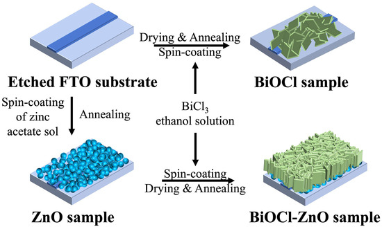
Figure 1.
Preparation process of the BiOCl–ZnO samples and the BiOCl sample.
Figure S1a,b display the top-view and cross-sectional SEM images of the pristine ZnO sample, respectively. The ZnO sample is an even and flat film consisting of densely packed nanoparticles. These nanoparticles show an average diameter of approximately 36.2 nm, and the average thickness of this ZnO film was estimated to be 170–180 nm. Figure 2 shows the morphologies and cross-sectional elemental mappings of the ZnO sample and a series of BiOCl-ZnO samples. Figure 2a–d presents the magnified top-view SEM images of the 1-, 2-, 3-, and 6-BiOCl-ZnO samples. The BiOCl layers are composed of vertical nanosheet arrays. The sizes of pores surrounded by BiOCl nanosheets in the 1- and 2-BiOCl-ZnO samples show no obvious difference. Notably, several BiOCl nanosheets protrude above the top BiOCl layer in the 1-BiOCl-ZnO sample, while the top BiOCl layer in the 2-BiOCl-ZnO sample has a significantly smoother surface. As the spin-coating time increases, the pore sizes formed by surrounding BiOCl nanosheets enlarge gradually in the 3- and 6-BiOCl-ZnO samples. Figure 2e–h show the cross-sectional SEM images of these BiOCl-ZnO samples, respectively. All these samples share a three-layered structure: the FTO substrate layer at the bottom, an intermediate ZnO nanoparticle layer, and a top BiOCl layer comprising vertically aligned BiOCl nanosheet arrays. The thicknesses of the top BiOCl layers are measured to be 184.4, 206.7, 284.9, and 430.2 nm in the 1-, 2-, 3-, and 6-BiOCl-ZnO samples, respectively. Consistent with the top-view SEM results, the 2-BiOCl-ZnO sample demonstrates superior surface flatness compared to the 1-BiOCl-ZnO sample.
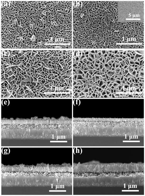
Figure 2.
Top-view SEM images of the (a) 1-BiOCl–ZnO, (b) 2-BiOCl–ZnO, (c) 3-BiOCl–ZnO, and (d) 6-BiOCl–ZnO samples. Cross-sectional SEM images of the (e) 1-BiOCl–ZnO, (f) 2-BiOCl–ZnO, (g) 3-BiOCl–ZnO, and (h) 6-BiOCl–ZnO samples.
Figure S2 displays the TEM characterization results of the hybrid separated from the 2-BiOCl-ZnO sample. It is seen in Figure S2a that the separated hybrid consists of several thin nanoplates, some of which are decorated with a few nanoparticles. The high-resolution TEM (HRTEM) image in Figure S2b is obtained from a sample area confined by the red rectangle. The clear lattice fringes of the corresponding nanoplate indicates its high crystallinity. One set of clear lattice fringes from the nanoplate with an interplanar lattice spacing of 0.257 nm corresponds to the (111) atomic planes of tetragonal BiOCl. The lateral size of these BiOCl nanoplates is much smaller than the nanosheets shown in the SEM images; it is deduced that the BiOCl nanosheets are formed by the compact accumulation of small nanoplates. A nanoparticle with a diameter of ≈30 nm, showing polycrystallinity, is anchored on the sharp edge of this nanoplate. The other sets of clear lattice fringes from this nanoparticle, decorated at the edge of the nanoplate with an interplanar lattice spacing of 0.280 nm, correspond to the (100) atomic planes of hexagonal ZnO. These results confirm the combination of ZnO nanoparticles with BiOCl nanosheets in the 2-BiOCl-ZnO sample.
Figure 3 presents the cross-sectional energy-dispersive X-ray spectroscopy (EDS) mapping results of the 2-BiOCl-ZnO sample. Its elemental mapping images in Figure 3a–e reveal distinct spatial segregation patterns. The oxygen element is uniformly distributed across all three layers, originating from the BiOCl in the top nanosheet array layer, the ZnO in the middle nanoparticle layer, and the SnO2 in the bottom FTO-coated substrate. Bismuth and chlorine elements are exclusively localized in the top BiOCl layer. The zinc element is predominantly confined to the ZnO layer in the middle. Moreover, gradual concentration gradients for all detected elements are found at the interfacial regions, demonstrating the successful formation of a heterojunction with continuous compositional transition and absence of abrupt interfacial discontinuities. The EDS spectrum of this sample in Figure 3f reveals the co-existence of O, Bi, Cl, and Zn elements.
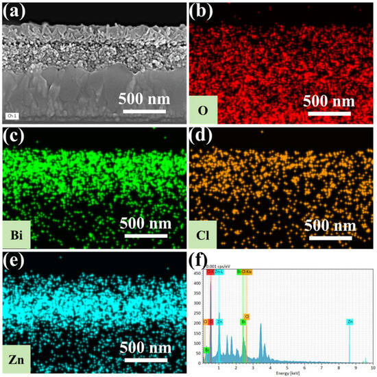
Figure 3.
(a) Cross-section SEM image, (b–e) elemental (O, Bi, Cl, and Zn) mappings, and (f) EDS spectrum of the 2-BiOCl-ZnO sample.
To investigate the influence of ZnO nanoparticle films on the growth process of BiOCl nanosheet arrays, a series of BiOCl nanosheet samples is prepared by the direct spin-coating of BiCl3 ethanol solution onto FTO substrates for different times, followed by the immersion in water and the subsequent annealing. With the times of spin-coating varying from 1, 2, 3, to 6 times, the corresponding BiOCl samples were labeled as 1-BiOCl, 2-BiOCl, 3-BiOCl, and 6-BiOCl. Figure S3 shows the morphologies and surface EDS characterization results of the 2-BiOCl sample. Figure S3a,b show the top-view and cross-sectional SEM images of the 2-BiOCl sample, respectively. It is revealed that several BiOCl nanosheets are stacked parallel or crosswise on the FTO surface to form an island-like distribution. The EDS elemental mapping images in Figure S3c–e demonstrate that Bi and Cl elements are enriched at the sites where BiOCl nanosheet stacks are, while the Sn element is concentrated in the other regions not covered by BiOCl nanostructures. In comparison, the BiOCl nanoflake arrays grown on ZnO films in the BiOCl-ZnO samples exhibit a smoother morphology and denser arrangement. This can be attributed to the closely packed ZnO nanoparticle layers, which provide abundant nucleation sites for BiOCl nanosheets. During the hydrolysis of BiCl3, a large number of BiOCl nanoflakes readily nucleate and grow, aligning uniformly along the well-ordered ZnO nanoparticle matrix. The EDS spectrum in Figure S3f confirms the coexistence of Bi, O, and Cl elements in the 2-BiOCl sample.
XRD patterns of the 2-BiOCl sample and 2-BiOCl-ZnO composite film samples are shown in Figure 4. The diffraction peaks of the 2-BiOCl thin film sample match well with the tetragonal phase BiOCl (PDF 99-000-0389). The peaks that emerged at 2θ of 25.97°, 32.6°, and 33.5° correspond to the (002), (101), and (110) crystal planes of the tetragonal BiOCl phase, respectively. For the 2-BiOCl-ZnO sample, the distinct diffraction peaks appear at 2θ of 31.8°, 34.6°, and 56.8°, which match well with the (100), (002), and (110) planes of hexagonal phase ZnO (PDF 97-006-5119), confirming the presence of well-crystallized hexagonal ZnO phase. The diffraction peaks of the BiOCl phase are also found in this 2-BiOCl-ZnO sample. However, the diffraction peaks originating from the BiOCl phase show reduced intensity and broadening, suggesting that the BiOCl nanosheets might consist of small-sized structural units or the strain effect originated from the confined nucleation and growth of BiOCl nanosheets in the formation of the BiOCl-ZnO heterojunction.
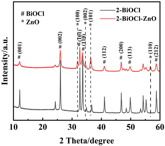
Figure 4.
XRD patterns of the 2-BiOCl and the 2-BiOCl–ZnO samples.
To analyze the surface composition and oxidation states of the composite film, XPS was performed on the 2-BiOCl-ZnO sample. The survey spectrum in Figure 5a confirms the presence of Zn, O, Cl, and Bi as the primary elements in this sample. The high-resolution Cl 2p spectrum in Figure 5b exhibits two characteristic peaks at 198.3 and 199.9 eV, corresponding to Cl 2p3/2 and Cl 2p1/2 in BiOCl, respectively, which verifies the existence of Cl− in BiOCl. As shown in Figure 5c, the binding energy peaks centered at 1022.1 and 1045.3 eV are attributed to Zn 2p3/2 and Zn 2p1/2, confirming the presence of Zn2+ in ZnO. The high-resolution O 1s spectrum in Figure 5d reveals two distinct binding energy peaks at 530.1 and 531.5 eV, which are assigned to lattice oxygen (O2−) and oxygen vacancy defects in the BiOCl-ZnO sample, respectively. Figure 5e displays the high-resolution Bi 4f spectrum, where the doublet binding energy peaks at 159.4 and 164.7 eV are indexed to Bi 4f7/2 and Bi 4f5/2, demonstrating the presence of Bi3+ in the BiOCl phase. Furthermore, signals from impurities, including metallic Bi0, are not detected, confirming the high purity of the 2-BiOCl-ZnO composite. These results provide evidence for the coexistence of BiOCl and ZnO in the composite sample, which is fully consistent with the XRD characterization results.
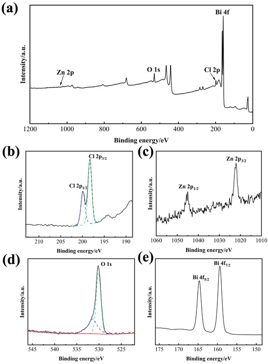
Figure 5.
XPS spectra of the 2-BiOCl-ZnO sample: (a) survey scan, (b) Cl 2p, (c) Zn 2p, (d) O 1s, and (e) Bi 4f spectrum.
Figure 6 presents the ultraviolet–visible diffuse reflectance spectroscopy (UV-Vis DRS) results of the ZnO and 2-BiOCl-ZnO composite samples. As shown in Figure 6a, the pure ZnO sample exhibits high UV light absorption and presents a sharp absorption edge near 405 nm. The optical band gaps of semiconductors could be determined using the Tauc plot method through the following equation [32],
where α, hν, A, Eg, and n denote the absorption coefficient, photon energy, constant of proportionality, band gap, and transition type constant, respectively. For the ZnO sample with a direct band gap, n = 1 is employed, and it estimates an intrinsic band gap of 3.25 eV, as indicated by the inset in Figure 6a. Meanwhile, the 2-BiOCl-ZnO sample demonstrates a notable red shift in absorption edge to 426 nm (Figure 6b), suggesting an extended responsive wavelength range via the incorporation of BiOCl nanosheet arrays. The Tauc plot of the pure BiOCl sample is shown in the inset of Figure 6b; its bandgap is calculated to be 3.32 eV.
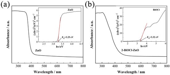
Figure 6.
UV-Vis DRS results of (a) the ZnO and (b) the 2-BiOCl-ZnO samples. The inserts are the Tauc plots of the ZnO and BiOCl samples.
Gold strip electrodes are deposited on the top of ZnO, BiOCl, and BiOCl-ZnO samples using thermal evaporation through templates. Silver pastes are doctor-bladed onto FTO strips in these samples to assemble the corresponding PDs. The photoelectric properties of these ZnO, BiOCl, and BiOCl-ZnO UV PDs were systematically investigated using a two-probe method, forming electrical contacts with the FTO and Au strip electrodes. Schematic diagrams of these three PD configurations are presented in the insets of Figure 7a–c. The dark current-voltage (I–V) characteristics of the FTO/ZnO/Au PD in Figure 7a and the FTO/BiOCl/Au PD in Figure 7b, as well as the I–V curves of the FTO/ZnO/Au PD under illumination in Figure S4, all exhibit symmetric linear relationships, confirming the formation of good ohmic contacts. The typical dark I–V curve of the 2-ZnO-BiOCl PD in Figure 7c demonstrates pronounced rectifying behavior with a rectification ratio of 21.67 at ±1 V, indicating its heterojunction nature, which primarily originates from the interfacial BiOCl-ZnO heterojunction. The energy band structure of the FTO/ZnO/BiOCl/Au heterojunction PD is proposed in Figure 7d via the comprehensive analysis of UV-Vis DRS results in Figure 6 and previous reports. The valence band (VB) and conduction band (CB) edge potentials of ZnO are estimated to be −7.6 eV and −4.35 eV, while those of BiOCl are −7.12 eV and −3.8 eV, respectively [33]. Upon the formation of a heterojunction, the Fermi levels of BiOCl and ZnO phases align at equilibrium. Because both the CB and VB edges of BiOCl are higher than those of ZnO, an efficient type-II heterojunction is formed at the BiOCl/ZnO interface, facilitating the effective spatial separation and transport of photoinduced charge carriers [34].
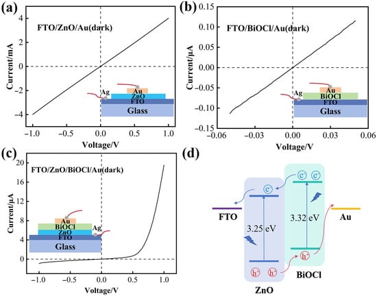
Figure 7.
I–V curves of (a) the FTO/ZnO/Au PD, (b) the FTO/BiOCl/Au PD, and (c) the FTO/ZnO/BiOCl/Au PD in the dark. (d) Schematic energy band structure of the FTO/ZnO/BiOCl/Au heterojunction PD.
To further investigate the photoelectric properties of the BiOCl-ZnO heterojunction PDs, Figure 8a compares the I–V characteristics of the BiOCl-ZnO heterojunction PD and ZnO PD in the dark and under 365 nm UV light illumination. Under zero bias, the ZnO PD generates a dark current of 2.3 μA, showing symmetric and linear curves regardless of illumination. After the growth of BiOCl nanosheet arrays on the ZnO nanoparticle film, all BiOCl-ZnO heterojunction PDs demonstrate rectifying behavior, with rectification ratios of 21.67 and 6.69 for 2- and 6-BiOCl-ZnO PDs at ±1 V, respectively. Compared with the ZnO PD, the 1-BiOCl-ZnO PD with one time of spin-coating shows a reduced dark current of 3.25 nA and an enhanced photocurrent of −11.18 μA at 0 V. The increase in spin-coating to two times reduces the dark current to 182 pA while boosting the photocurrent to −26.93 μA in the 2-BiOCl-ZnO PD. For the thick BiOCl layer formed by six times of spin-coating, the 6-BiOCl-ZnO PD maintains a relatively low dark current of 0.64 nA, which is slightly higher than the 2- and 3-BiOCl-ZnO devices but significantly lower than both the ZnO PD and 1-BiOCl-ZnO PD. The thinner BiOCl layers with 1–3 times of spin-coating enable carrier transport primarily through thermionic emission over the potential barrier, showing substantially lower dark current compared to pure ZnO and thicker BiOCl films. The thicker BiOCl layer with 6 times the spin-coating contains more pronounced defect states that may provide additional thermal excitation channels, slightly compromising the suppression effect of the interfacial built-in electric field on the dark current. Nevertheless, the lower dark current of 6-BiOCl-ZnO PD compared to ZnO PD confirms the effectiveness of the heterojunction, attributed to the increased grain boundaries and non-uniform stacking of nanosheets in thicker BiOCl layers. Figure 8b presents the current-voltage characteristics of the 2-BiOCl-ZnO PD in the dark and under illumination at various wavelengths. This PD exhibits pronounced rectifying behavior in the dark, with current rapidly increasing under forward bias while being effectively suppressed under reverse bias, yielding a rectification ratio of 21.67 and proving the formation of a heterojunction between ZnO and BiOCl phases. Under 365 nm UV light illumination, the photocurrent of this device shows remarkable enhancement, particularly in the reverse bias region, indicating efficient separation of photogenerated carriers driven by the electric field in the depletion region. When illuminated by other UV light (290 and 310 nm) and visible light (405, 450, 515, and 550 nm) illuminations, the measured photocurrents are weaker than those generated at 365 nm but remain significantly higher than the dark current. These results demonstrate the broadband spectral response of 2-BiOCl-ZnO PD enabled by the incorporation of BiOCl. The gradual decrease in photocurrent from 365 to 550 nm aligns with the bandgap matching of the BiOCl-ZnO heterojunction, confirming the dominant role of UV light excitation in the photo-induced carrier generation process. Notably, this device generates a photocurrent of 23.55 μA at zero bias and 365 nm, demonstrating its self-powered photodetection capability. Figure 8c,d display the time-dependent current responses of the ZnO PD, various BiOCl PDs, and the BiOCl-ZnO heterojunction PDs under 365 nm illumination and at zero bias. Both the ZnO PD and BiOCl PDs present significant persistent photoconductivity (PPC) effects, characterized by the slow rise in currents upon illumination and incomplete recovery to the initial level of dark currents after the end of light illumination. In comparison, the BiOCl-ZnO heterojunction PDs demonstrate typical transient photoconductivity behavior, with rapid saturation of photocurrents upon illumination and their complete recovery to the dark state within 20 ms after the termination of light illumination. The ZnO PD shows a gradual increase in photocurrent to 1.47 μA after 20 s of light illumination, followed by a slow decay of current to 2.05 μA within 20 s after the light is off, resulting in a negligible on/off ratio of 0.718. Meanwhile, the 1-BiOCl-ZnO PD achieves a photocurrent of −11.18 μA. The introduction of BiOCl nanosheet arrays dramatically reduces the dark current while significantly enhancing the photocurrent, leading to a much higher on/off ratio of 1245. The 2-BiOCl-ZnO PD shows further improved photoelectric performance, with its photocurrent elevated to −26.93 µA and the on/off ratio increased to 22,748. However, as the spin-coating times increase, the photocurrents of 3- and 6-BiOCl-ZnO PDs decrease to −7.36 and −4.54 µA, respectively. Their on/off ratios have declined successively to 5984 and 3916. Importantly, all these BiOCl-ZnO PDs exhibit excellent current reproducibility in response to the repeated light on/off switching cycles, confirming their outstanding operational stability.
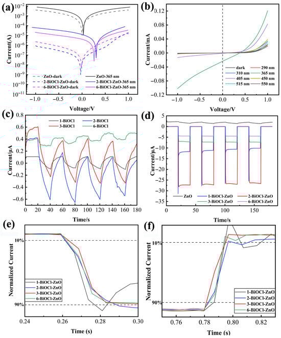
Figure 8.
Photoelectric performance comparison between the ZnO PD, the BiOCl PDs, and the BiOCl-ZnO heterojunction PDs: (a) I–V characteristics of the PDs in dark and under 365 nm light illumination; (b) I–V curves of the 2-BiOCl-ZnO PD under different wavelength light illumination; I–t characteristics of (c) the BiOCl PDs and (d) ZnO PD and BiOCl-ZnO PDs at 0 V and under 365 nm light illumination; normalized (e) rising and (f) recovery I–t curves of the BiOCl-ZnO PDs.
Rapid response to light illumination is fundamental to high-performance PDs. To investigate the influence of BiOCl nanosheet arrays on the response speed of heterojunction PDs, the normalized I–t curves of the ZnO PD and ZnO-BiOCl PDs are presented in Figure 8e,f. The rise time is defined as the duration required for the current to increase from 10% to 90% of its peak value, while the recovery time corresponds to the period required for the current to decrease from 90% to 10% of the peak value. Both the rise and decay times of the ZnO PD exceed 20 s. The 1-BiOCl-ZnO PD demonstrates significantly improved performance with a greatly reduced rise time of 15.80 ms and a dramatically shortened decay time of 14.32 ms. The 2-BiOCl-ZnO PD shows a comparable rise/decay time of 17.44 ms/14.00 ms. Meanwhile, the 3- and 6-BiOCl-ZnO PDs exhibit rise times of 18.98 and 20.46 ms, accompanied by decay times of 13.59 and 10.54 ms, respectively. These results demonstrate that the built-in electric field formed at the BiOCl-ZnO heterojunction interface facilitates the efficient carrier separation and rapid recombination, thereby accelerating both the fast increase and rapid decay of photocurrent. The improvements in response times underscore the critical role of heterojunction engineering in achieving high-speed photodetection.
The spectral responsivity (Rλ), as a fundamental figure of merit for PDs, quantifies the electrical response to monochromatic illumination [35]. It is defined by
where Iph represents photocurrent, Id denotes dark current, P is the optical power density, and S indicates the effective illumination area. Figure 9a presents the spectral response of the ZnO PD and BiOCl-ZnO PDs under zero bias across 350–450 nm. All these devices exhibit pronounced photoresponse from 350 to 390 nm; they also present gradually decreasing sensitivity toward longer wavelengths, demonstrating excellent UV selectivity. Notably, the 1-BiOCl-ZnO PD shows significantly enhanced responsivity compared to the ZnO PD in the UV region of 350–390 nm. Under zero bias, the ZnO PD achieves a responsivity of 6.2 mA·W−1 at 350 nm, while the peaks of responsivity curves for all the BiOCl-ZnO PDs appear near 354 nm. The 2-BiOCl-ZnO PD demonstrates a maximum responsivity of 1082.60 mA·W−1 at 365 nm, representing a 174-fold improvement over the ZnO PD. It is believed that the high surface-area-to-volume ratio of BiOCl nanosheet arrays facilitates the formation of abundant ZnO/BiOCl heterointerfaces, dramatically improving carrier separation efficiency and resulting in improved responsivities. However, excessive thicknesses of BiOCl layers in the 3- and 6-BiOCl-ZnO PDs induce the losses of light scattering and overall light absorption, consequently reducing their photoresponse. The photoconductive behavior of this device is investigated under 365 nm light illumination with power densities ranging from 2.20 to 98.4 mW·cm−2. As shown in Figure 9b, the photocurrents generated by all these BiOCl-ZnO PDs are increased with light intensities. For the 2-BiOCl-ZnO PD, the photocurrent at zero bias evolves from −0.012 µA (2.2 mW·cm−2) to −23.28 µA (98.4 mW·cm−2), following the fundamental relationship between the efficiency of carrier generation and photon flux. The photocurrent-light intensity relationship of PDs generally obeys the power law,
where A is a constant and θ (0.5 < θ < 1) determines the linearity of response with power density (P). It reveals excellent linearities for the 2-BiOCl-ZnO (θ = 0.996) and 3-BiOCl-ZnO PDs (θ = 0.962), suggesting their potentials for precision photometry. Whereas the 1-BiOCl-ZnO (θ = 0.542) and 6-BiOCl-ZnO PDs (θ = 0.719) show sublinear behavior, reflecting complex carrier dynamics at the BiOCl/ZnO heterointerfaces.
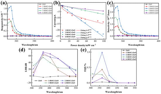
Figure 9.
(a) Spectral response of the PDs at 0 V bias. (b) Corresponding fitting curves for the relationship between photocurrent of the PDs and light intensity. (c) Detectivity curves, (d) linear dynamic range spectra, and (e) EQE curves of the BiOCl–ZnO PDs at 0 V bias.
Specific detectivity (D*, Jones) [36] and linear dynamic range (LDR, dB) [37], as two critical figures of merit for PDs, are systematically evaluated and recorded in Figure 9c and Figure 9d, respectively. D* represents the signal-to-noise performance and is calculated as,
The 2-BiOCl-ZnO PD achieves the highest D* value of 2.48 × 10¹³ Jones at 354 nm in the wavelength range from 350 to 390 nm, owing to its suppressed dark current and enhanced responsivity. All heterojunction PDs outperform the ZnO PD in detectivity, proving the advantage of heterostructure engineering. LDR demonstrates the operational range for weak-signal detection and is defined as,
The ZnO PD shows negative LDR (Iph < Id) in the wavelength range of 310–450 nm, all BiOCl-ZnO PDs exhibit LDR values larger than 50 dB at 365 nm. The LDR value of 6-BiOCl-ZnO PD at 365 nm reaches 71.56 dB, indicating their potential application in complex lighting conditions.
External quantum efficiency (EQE) indicates the conversion efficiencies of PDs from light energy to electrical energy, which can be calculated as,
Compared with a low EQE value (0.03%) of the ZnO PD at 365 nm, the EQE values of the BiOCl-ZnO PDs were significantly improved, and the corresponding EQE-wavelength curves are depicted in Figure 9e. Most of the BiOCl-ZnO PDs generate the highest EQE at 365 nm, and the highest EQE value of 0.99% is achieved by the 2-BiOCl-ZnO PD.
Table 1 compares the key performance parameters of various PDs under 365 nm light illumination and zero bias. The results highlight that the heterojunction formed between BiOCl nanosheets and ZnO nanoparticles improves the photodetection capabilities. Particularly, the 2-BiOCl-ZnO PD achieves an optimal balance between light absorption and carrier behavior management, delivering the best performance. This work establishes that nanostructured heterointerfaces can simultaneously enhance the responsivity, detectivity, and operational dynamic range of PDs.

Table 1.
Performance parameters of the ZnO PD and different BiOCl-ZnO heterojunction PDs operating at 0 V bias and under 365 nm light illumination.
Table 2 compares the photoelectric performance of BiOCl-ZnO with other previously reported and related heterostructures. The BiOCl–ZnO heterojunction PD exhibited better performance than other related PDs.
Table 2.
Comparison of the PD performance of 2-BiOCl-ZnO with other reported heterostructures.
Owing to its self-powered operation, rapid response, and high on/off ratio, the optimized BiOCl-ZnO heterojunction PD demonstrates promising potential as a message receiver in an optical communication system displayed in Figure 10a. At the beginning of light communication, the message is coded by the signal source according to the binary encoding protocol, which outputs a series of continuous electrical signals. The output electrical signal is utilized to control the on/off states of the 365 nm laser in a certain period of time, generating a series of light signals conveying a message. After being transferred by an optical fiber, the as-generated 365 nm light signals are illuminated on the PD. The electrical signals output by this PD are amplified by an amplifier and then processed by the data acquisition (DAQ) device. The electrical signals are encoded according to the binary encoding protocol and recovered to the original message. As shown in the code-interpretation parallel table in Figure 10b, every eight binary number bits constitute one byte. Three specific bytes, “00000100”, “00000100”, and “00100000”, symbolize the start of the message, the end of the message, and the space between words in the message, respectively. For the 2-ZnO-BiOCl PD acting as the message receiver, the photocurrent generated under 365 nm laser illumination in a fixed interval represents one bit named “1”, while its dark current in the same interval signifies one bit named “0”. Using this optical switching scheme, the 2-ZnO-BiOCl PD successfully decodes the transmitted message to “Hello NWPU!”, as presented in Figure 10c. This PD’s sub-20 ms response time is shorter than the on/off state switching duration of 0.1 s for the 365 nm laser, achieving a transmission rate of 10 bit·s−1 and effectively preventing inter-symbol interference. The exceptional on/off ratio (>104) combined with the ultralow dark current of this PD ensures reliable signal discrimination at this data rate. Moreover, the self-powered properties of this PD eliminate the requirement of an external power source, substantially reducing the receiver-end power consumption and extending the operational endurance. Remarkably, this PD exhibits near-ideal linear response characteristics (θ > 0.99), enabling precise discrimination of eight distinct intensity levels for advanced modulation schemes. This capability permits 3-bit information encoding per byte, theoretically tripling the data throughput compared to binary transmission. When employing such multilevel signaling, the device’s short response time theoretically supports transmission rates up to 50 bit·s−1 in optimized systems.
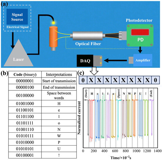
Figure 10.
BiOCl-ZnO heterojunction PD adopted in an optical communication system: (a) schematic diagram, (b) code-interpretation parallel table, and (c) I–V curve generated by the PD and utilized for message transmitting.
4. Conclusions
In summary, mixed-dimensional heterojunction PDs based on 3D BiOCl nanosheet arrays and 2D ZnO nanoparticle films were successfully fabricated through simple spin-coating and soaking methods. Compared to the pristine ZnO PD exhibiting large dark current (≈2 μA), low photocurrent (≈1.5 μA), and slow response/decay times (>20 s), the optimized 2-BiOCl-ZnO heterojunction PD demonstrates significantly improved performance under 365 nm light illumination (104 mW·cm−2) at zero bias, including dramatically reduced dark current (≈1 nA), ultrahigh on/off ratio (2.275 × 10⁴), and short rise/decay time (17.44 ms/14 ms). This device also achieves an outstanding responsivity (1082.6 mA·W−1), a high detectivity (2.48 × 10¹³ Jones) at 354 nm, as well as a large linear dynamic range (67.62 dB) and EQE value (0.99%) at 365 nm, representing its substantially improved photoelectric performance over the ZnO PD. The enhanced performance originates from the built-in electric field formed at the BiOCl-ZnO heterojunction interface, the improved light absorption enabled by the nanosheet array morphology of BiOCl, and the optimized charge carrier separation and transport within the device. Additionally, the addition of optimized BiOCl nanostructures contributes to extra photon absorption and generation of electron-hole pairs that are effectively separated by the built-in field, further increasing the responsivities over the extended responsive wavelength range. However, BiOCl nanosheet arrays with excessive thickness can reduce the light absorption and carrier transport, leading to degraded photoelectric performance. The optimized 2-BiOCl-ZnO heterojunction PD also demonstrates its usage as a self-powered receiver in a high-speed optical communication system, making it promising for UV light communication applications. The rational construction of BiOX-based heterojunction has been proven as an efficient way to achieve self-powered photodetection.
Supplementary Materials
The following supporting information can be downloaded at: https://www.mdpi.com/article/10.3390/pr13113428/s1, Figure S1: (a) top-view and (b) cross-sectional images of the ZnO sample; Figure S2: (a) TEM images and (b) HRTEM image of the hybrid separated from the 2-BiOCl-ZnO sample; Figure S3: (a) top view and (b) cross-sectional SEM images; (c–e) elemental mapping (Bi, Sn, and Cl), and (f) EDS spectrum of the 2-BiOCl sample; Figure S4: I–V curves of the ZnO PD under different wavelength light illumination.
Author Contributions
Writing—original draft preparation, M.Z.; Methodology, W.O.; Investigation, M.Z.; Writing—review and editing, W.O.; Supervision, W.O. All authors have read and agreed to the published version of the manuscript.
Funding
This research was funded by the National Natural Science Foundation of China (52202187), the Natural Science Basic Research Program of Shaanxi Province (2022JQ-352), and the Fundamental Research Funds for the Central Universities (D5000210579).
Data Availability Statement
The original contributions presented in this study are included in the article/Supplementary Materials. Further inquiries can be directed to the corresponding authors.
Conflicts of Interest
The authors declare no conflicts of interest.
Abbreviations
The following abbreviations are used in this manuscript:
| PD | Photodetector |
| FTO | Fluorine-doped tin oxide |
| DRS | Diffuse reflectance spectroscopy |
| EDS | Energy-dispersive X-ray spectroscopy |
| XRD | X-ray diffraction |
| SEM | Scanning electron microscopy |
| XPS | X-ray photoelectron spectroscopy |
| PPC | Photoconductivity |
| LDR | Linear dynamic range |
| DAQ | Data Acquisition |
References
- Guo, L.; Guo, Y.; Wang, J.; Wei, T. Ultraviolet communication technique and its application. J. Semicond. 2021, 42, 081801. [Google Scholar] [CrossRef]
- Abdullah, M.; Younis, M.; Sohail, M.T.; Wu, S.; Zhang, X.; Khan, K.; Asif, M.; Yan, P. Recent progress of 2D materials-based photodetectors from UV to THz waves: Principles, materials, and applications. Small 2024, 20, 2402668. [Google Scholar] [CrossRef]
- Rogalski, A.; Bielecki, Z.; Mikołajczyk, J.; Wojtas, J. Ultraviolet photodetectors: From photocathodes to low-dimensional solids. Sensors 2023, 23, 4452. [Google Scholar] [CrossRef] [PubMed]
- Ouyang, W.; Zhang, M. Electrode materials and structures in UV photodetectors. Appl. Phys. Rev. 2024, 11, 031309. [Google Scholar] [CrossRef]
- Xing, R.; Zhang, X.; Fan, X.; Xie, R.; Wu, L.; Fang, X. Coupling strategies of multi-physical fields in 2D materials-based photodetectors. Adv. Mater. 2025, 37, 2501833. [Google Scholar] [CrossRef]
- Fang, X.; Hu, L.; Huo, K.; Gao, B.; Zhao, L.; Liao, M.; Chu, P.K.; Bando, Y.; Golberg, D. New ultraviolet photodetector based on individual Nb2O5 nanobelts. Adv. Funct. Mater. 2011, 21, 3907–3915. [Google Scholar] [CrossRef]
- Deka Boruah, B. Zinc oxide ultraviolet photodetectors: Rapid progress from conventional to self-powered photodetectors. Nanoscale Adv. 2019, 1, 2059–2085. [Google Scholar] [CrossRef]
- Hullavarad, S.; Hullavarad, N.; Look, D.; Claflin, B. Persistent photoconductivity studies in nanostructured ZnO UV sensors. Nanoscale Res. Lett. 2009, 4, 1421–1427. [Google Scholar] [CrossRef] [PubMed]
- Jiang, G.; Zhao, D.; Zhao, B. ZnO nanowire UV photodetector with multiple channels. Microelectron. Int. 2018, 35, 18–23. [Google Scholar] [CrossRef]
- Peng, Y.; Jiang, D.; Zhao, M.; Duan, Y.; Wei, H.; Li, H.; Liang, Q.; Wang, S. High-performance UV–visible photodetectors based on ZnO/perovskite heterostructures. J. Alloy. Compd. 2023, 965, 171372. [Google Scholar] [CrossRef]
- Chantarat, N.; Chen, Y.W.; Chen, S.Y.; Lin, C.C. Enhanced UV photoresponse in nitrogen plasma ZnO nanotubes. Nanotechnology 2009, 20, 395201. [Google Scholar] [CrossRef][Green Version]
- Chai, G.; Lupan, O.; Chow, L.; Heinrich, H. Crossed zinc oxide nanorods for ultraviolet radiation detection. Sensor. Actuat. A Phys. 2009, 150, 184–187. [Google Scholar] [CrossRef]
- Ouyang, W.; Chen, J.; Shi, Z.; Fang, X. Self-powered UV photodetectors based on ZnO nanomaterials. Appl. Phys. Rev. 2021, 8, 031315. [Google Scholar] [CrossRef]
- Jin, Y.; Wang, J.; Sun, B.; Blakesley, J.C.; Greenham, N.C. Solution-processed ultraviolet photodetectors based on colloidal ZnO nanoparticles. Nano Lett. 2008, 8, 1649–1653. [Google Scholar] [CrossRef]
- Yang, H.Y.; Son, D.I.; Kim, T.W.; Lee, J.M.; Park, W.I. Enhancement of the photocurrent in ultraviolet photodetectors fabricated utilizing hybrid polymer-ZnO quantum dot nanocomposites due to an embedded graphene layer. Org. Electron. 2010, 11, 1313–1317. [Google Scholar] [CrossRef]
- Gao, Z.; Chen, L.; Li, S.; Pan, X.; Liu, Y.; Gao, G.; Zou, B. Type-II CsPbBr3/ZnS heterostructured nanocrystals for high-performance self-powered photodetector. ACS Appl. Nano Mater. 2025, 8, 5623–5631. [Google Scholar] [CrossRef]
- Cao, H.-X.; Yao, C.-B.; Li, H.-Y.; Shi, B.-Y.; Zheng, X.-Y.; Liu, Y.; Yin, H.-T. Band gap and interface engineering of ZnO@MoSe2 heterojunction film and its light-matter coupling. Opt. Mater. 2023, 136, 113410. [Google Scholar] [CrossRef]
- Lin, H.; Jiang, A.; Xing, S.; Li, L.; Cheng, W.; Li, J.; Miao, W.; Zhou, X.; Tian, L. Advances in self-powered ultraviolet photodetectors based on P-N heterojunction low-dimensional nanostructures. Nanomaterials 2022, 12, 910. [Google Scholar] [CrossRef] [PubMed]
- Chen, Y.; Zhang, L.; Peng, X.; Qin, W.; Li, S.; Wang, Y.; Chen, Z.; Xiao, S.; Yang, B.; Liu, B.; et al. Epitaxial quasi-2D/3D hybrid perovskite heterojunctions for photodetector with enhanced detectivity and stability. Nano Res. 2024, 17, 6594–6602. [Google Scholar] [CrossRef]
- Ni, S.; Guo, F.; Wang, D.; Liu, G.; Xu, Z.; Kong, L.; Wang, J.; Jiao, S.; Zhang, Y.; Yu, Q.; et al. Effect of MgO surface modification on the TiO2 nanowires electrode for self-powered UV photodetectors. ACS Sustain. Chem. Eng. 2018, 6, 7265–7272. [Google Scholar] [CrossRef]
- Ma, Y.; Wu, M.; Wan, P.; Jiang, M.; Li, Z.; Cui, Q.; Shi, Z.; Wang, X.; Xu, C. One-dimensional ZnO/AlN core-shell interface design for pure ultraviolet electroluminescence. J. Light. Technol. 2025, 43, 4352–4357. [Google Scholar] [CrossRef]
- Deng, Z.; Liang, Z.; Yang, Y.; Ye, Q.; Ning, H.; Liu, X.; Li, Z.; Luo, D.; Yao, R.; Peng, J. Heterojunction channel engineering for enhanced mobility and stability of solution-processed holmium-doped indium oxide thin film transistors. Mater. Sci. Semicond. Process. 2024, 184, 108776. [Google Scholar] [CrossRef]
- Dutta, A.; Medda, A.; Patra, A. Recent advances and perspectives on colloidal semiconductor nanoplatelets for optoelectronic applications. J. Phys. Chem. C 2020, 125, 20–30. [Google Scholar] [CrossRef]
- Jena, D.; Fang, T.; Zhang, Q.; Xing, H. Zener tunneling in semiconducting nanotube and graphene nanoribbon p-n junctions. Appl. Phys. Lett. 2008, 93, 112106. [Google Scholar] [CrossRef]
- Ahn, J.; Yeon, E.; Hwang, D.K. Recent progress in 2D heterostructures for high-performance photodetectors and their applications. Adv. Opt. Mater. 2025, 13, 2403412. [Google Scholar] [CrossRef]
- Chen, J.; Ouyang, W.; Yang, W.; He, J.H.; Fang, X. Recent progress of heterojunction ultraviolet photodetectors: Materials, integrations, and applications. Adv. Funct. Mater. 2020, 30, 1909909. [Google Scholar] [CrossRef]
- Chen, Y.; Wang, R.; Gao, H.; Huang, H.; Dong, R.; Lu, C.; Kou, J. Elevating the photocatalytic performance of BiOCl by promoting llight utilization: From Co doping to the microreactor. J. Phys. Chem. Lett. 2024, 15, 1412–1419. [Google Scholar] [CrossRef]
- Kondusamy, A.L.N.; Liu, W.; Roy, J.; Zhu, X.; Smith, C.V.; Wang, X.; Young, C.; Kim, M.J.; Wallace, R.M.; Vandenberghe, W.G.; et al. Bismuth oxychloride as avan der Waals dielectric for 2D electronics. Nanotechnology 2025, 36, 185201. [Google Scholar] [CrossRef]
- Wang, J.; Chu, Q.; Xu, M.; Gong, Y.; Feng, Y.; Meng, M.; Gao, M. Construction of a BiOCl/Bi2O2CO3 S-scheme heterojunction photocatalyst via sharing [Bi2O2]2+ slabs with enhanced photocatalytic H2O2 production performance. Langmuir 2024, 40, 15456–15467. [Google Scholar] [CrossRef]
- Teng, F.; Ouyang, W.; Li, Y.; Zheng, L.; Fang, X. Novel structure for high performance UV photodetector based on BiOCl/ZnO hybrid film. Small 2017, 13, 1700156. [Google Scholar] [CrossRef]
- Ouyang, W.; Teng, F.; Fang, X. High performance BiOCl nanosheets/TiO2 nanotube arrays heterojunction UV photodetector: The influences of self-Induced inner electric fields in the BiOCl nanosheets. Adv. Funct. Mater. 2018, 28, 1707178. [Google Scholar] [CrossRef]
- Sangiorgi, N.; Aversa, L.; Tatti, R.; Verucchi, R.; Sanson, A. Spectrophotometric method for optical band gap and electronic transitions determination of semiconductor materials. Opt. Mater. 2017, 64, 18–25. [Google Scholar] [CrossRef]
- Ouyang, W.; Chen, J.; He, J.H.; Fang, X. Improved photoelectric performance of UV photodetector based on ZnO nanoparticle-decorated BiOCl nanosheet arrays onto PDMS substrate: The heterojunction and Ti3C2Tx MXene conduction layer. Adv. Electron. Mater. 2020, 6, 2000168. [Google Scholar] [CrossRef]
- Dutta, A.; Medda, A.; Bera, R.; Rawat, A.; De Sarkar, A.; Patra, A. Electronic band structure and ultrafast carrier dynamics of two dimensional (2D) semiconductor nanoplatelets (NPLs) in the presence of electron acceptor for optoelectronic applications. J. Phys. Chem. C 2020, 124, 26434–26442. [Google Scholar] [CrossRef]
- Zhao, B.; Wang, F.; Chen, H.; Wang, Y.; Jiang, M.; Fang, X.; Zhao, D. Solar-blind avalanche photodetector based on single ZnO-Ga2O3 core-shell microwire. Nano Lett. 2015, 15, 3988–3993. [Google Scholar] [CrossRef] [PubMed]
- Dou, L.; Yang, Y.M.; You, J.; Hong, Z.; Chang, W.H.; Li, G.; Yang, Y. Solution-processed hybrid perovskite photodetectors with high detectivity. Nat. Commun. 2014, 5, 5404. [Google Scholar] [CrossRef]
- García de Arquer, F.P.; Armin, A.; Meredith, P.; Sargent, E.H. Solution-processed semiconductors for next-generation photodetectors. Nat. Rev. Mater. 2017, 2, 16100. [Google Scholar] [CrossRef]
- Su, L.; Ouyang, W.; Fang, X. Facile fabrication of heterostructure with p-BiOCl nanoflakes and n-ZnO thin film for UV photodetectors. J. Semicond. 2021, 42, 052301. [Google Scholar] [CrossRef]
- Huang, J.; Jiang, J.; Hu, L.; Zeng, Y.; Ruan, S.; Ye, Z.; Zeng, Y.-J. Self-powered ultraviolet photodetector based on CuGaO/ZnSO heterojunction. J. Mater. Sci. 2020, 55, 9003–9013. [Google Scholar] [CrossRef]
- Zhang, Q.; Xu, J.; Li, M.; Chen, J.; Xu, J.; Zheng, Q.; Shi, S.; Kong, L.; Zhang, X.; Li, L. High-performance self-powered ultraviolet photodetector based on BiOCl/TiO2 heterojunctions: Carrier engineering of TiO2. Appl. Surf. Sci. 2022, 592, 153350. [Google Scholar] [CrossRef]
- Kumari, R.; Kumar, A.; Dahiya, S.; Srivastava, S.K.; Guin, D.; Tripathi, C.S.P. A highly responsive UV photodetector based on WO3–ZnO layered thin film. Opt. Mater. 2025, 166, 117205. [Google Scholar] [CrossRef]


Disclaimer/Publisher’s Note: The statements, opinions and data contained in all publications are solely those of the individual author(s) and contributor(s) and not of MDPI and/or the editor(s). MDPI and/or the editor(s) disclaim responsibility for any injury to people or property resulting from any ideas, methods, instructions or products referred to in the content. |
© 2025 by the authors. Licensee MDPI, Basel, Switzerland. This article is an open access article distributed under the terms and conditions of the Creative Commons Attribution (CC BY) license (https://creativecommons.org/licenses/by/4.0/).