Abstract
In recent times, important contributions and the incorporation of renewable sources, such as photovoltaic, fuel cells, etc., are the main reasons for the popularity of DC microgrids. Integrating renewable sources into the microgrid requires high-voltage, high-efficiency DC-to-DC converters. Without modification, traditional converters are not suitable for achieving the required voltage in microgrid applications, due to the requirement for a large duty cycle, inductor resistance, voltage rating of switches, reverse recovery of the diode, high current rating inductors, etc. Various converters based on the circuitry of voltage multipliers, switched inductors/capacitors, coupled inductors, transformers, etc., have been proposed in the literature and have their drawbacks. In this paper, to realize significant voltage gain with two duty cycle controls, a new multi-leg (ML) converter is recommended as a solution for use in DC microgrids. The converter is designed by incorporating multiple legs into the boost converter. The implications of the proposed converter are reduced device voltage stress, small inductors and capacitors, two-duty cycle control, triple mode operation, single-stage conversion, etc. The proposed converter’s power circuits, mode of operation, and design equations of the converter are presented. The non-ideal model of the proposed converter is discussed, and efficiency is analyzed. The effect of unequal insurance on the operation of the converter is discussed. Comparative studies of converters are provided to draw attention to the benefits of the converter. The results of the experiments are shown to prove that the analysis and performance of the converter are correct. The discontinuous mode of operation and unequal inductance case of the converter are studied with the help of a simulation model.
1. Introduction
Many nations concentrate on renewable energy systems, which are more reliable, less costly, produce no poisonous by-products during operation, and are abundant in nature. In comparison to the voltage of the DC link, the output voltage of renewable sources, such as photovoltaic and fuel cell systems, is relatively low [1,2]. The sustainable development goals in the Envision 2030 agenda of the United Nations will pave the way for a promising future for renewable energy. The Saudi Vision 2030 is consistent with these objectives. The sustainable development goals (SDG) in the Envision 2030 agenda of the United Nations will pave the way for a promising future for renewable energy. The Saudi Vision 2030 is consistent with these objectives. SDG 7 of the United Nations is a sustainable, affordable energy system, which is supported by the suggested work goals. This effort promises to provide a good, energy-efficient system by employing a new DC–DC converter (SDG 12). The authors employed methods known as “double duty control” to achieve this (SDG 9). The structure of a usual microgrid operating at 400V DC is depicted in Figure 1. Research of a more advanced nature is being conducted in order to develop a more advanced interface system for the purpose of integrating renewable energy sources with the existing microgrid. This is in response to the growing demand for renewable energy sources within the existing microgrid [3,4]. The DC–DC converters are employed to integrate different power sources with the DC bus available in a microgrid [5,6]. The advancement of loads used in the current microgrid results in the requirement of a higher voltage source to drive them, whereas the voltage generated by renewable energy sources is insufficient to power those loads. In order to feed the DC and AC loads from the power generated by renewable energy sources, power electronics converters are employed [7,8]. The employment of DC–DC converters in emerging research fields, such as intelligent systems, electric-car fast-charging systems, and spacecraft applications have led researchers to concentrate more on DC–DC converter research areas. While developing improved DC–DC converters, different properties, such as high gain, high power delivery capability, compactness in size, converters with fewer component counts, less electromagnetic interference, fewer switches, etc., are mainly focused on [9,10]. Obtaining a higher gain voltage from the conventional DC–DC converters is possible, theoretically. However, practically operating a converter with a duty ratio of ≥0.9 is highly impossible, as it leads to high instability of the voltage at the output of the converter [11,12]. Moreover, parasitic elements in the converters restrict their usage to obtain a higher voltage gain. The invention of an isolated/non-isolated converter using a transformer or coupled inductor led researchers to obtain higher voltage gain [13,14]. Isolated power converters use a transformer to physically and electrically separate the input and output of the circuit so that no direct current can flow between them. When a transformer is turned on for the first time or after a short break, the core magnetization may not be in sync with the voltage. This can cause the transformer to draw inrush current from the system. Positive voltage creates positive flux, which adds to the residual flux already on the transformer core (remember, flux is the time integral of the voltage). The core is quickly saturated as a result of this. The effective magnetizing branch reduces the transformer’s air-core impedance. The air-core impedance is about the same size as the leakage impedance of the transformer. The effective impedance is controlled by flux; thus, when the transformer core saturates, the small impedance pulls a high-magnitude current from the system. The core saturates in one direction, so the transformer draws pulses of the inrush current with a strong DC component. In general, isolated converters follow DC–AC and AC–DC conversion steps. The two-step power-conversion process, core loss, and leakage magnetic power loss lead to an increase in total system loss. Moreover, the formation of a high inrush current at the primary side increases the size of the input filter. The isolated converter system was cumbersome and expensive due to the fact that it utilized a transformer [15,16]. The voltage gain in the coupled inductor-based topologies is based on the coupling factor, number of turns, and duty ratio. Therefore, we can achieve the desired voltage gain by selecting appropriate turns of the coupling inductor and controlling the duty ratio. In [17], a converter based on the coupling of two inductors is presented to achieve voltage gain , where D is the duty cycle and n is coupling ratio. However, this circuitry required an additional clamp circuit to absorb the leakage of energy. In [18], a zero-voltage-switching converter based on the coupling of two inductors and one normal inductor is presented with high efficiency and voltage gain . Nevertheless, to get rid of the voltage spike, this circuitry needed an active clamp circuit. In [19], a coupled inductor-based converter with minimal reverse recovery of the output diode and the ability to achieve voltage gain is presented. However, to construct this converter, an auxiliary boosting circuit including snubber circuitry is required. Therefore, to suppress the switch voltage spike caused due to leakage inductance, an auxiliary voltage clamp and a snubber circuit are applied, which increases the cost and size. Several other converters based on coupled inductors and other boosting techniques are discussed with advantages and disadvantages in [20].
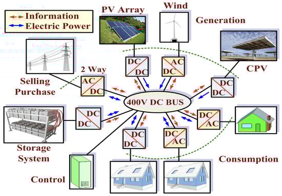
Figure 1.
Typical microgrid structure with 400 V DC bus.
Adding converters in series is a straightforward method to boost the voltage with high voltage gain. A cascaded converter is created when two or more boost converters of the same or different types are linked together [20,21,22]. However, in this, the energy is transferred from one block to another block, which results in lower efficiency since the complete efficiency is the multiplication of the efficiency of each block. For example, the first-stage stored energy transfers to the second stage, the second stage to the third stage, and so on, and the final last stage energy delivers to the load. Moreover, the voltage gain is more nonlinear, and slight changes in the duty affect the output voltage more. Thus, a precise intricate control technique is required. The rating of the reactive components progressively increases from the first stage to the last stage. Moreover, the current and voltage ratings of the components and devices also need to be higher as the total number of stages increases. Revolution in converter research leads to the invention of the switched capacitor converters as a replacement for the cascaded converters, which can provide both step-up/down voltage conversion ratios [23,24]. In the conventional switched capacitor method, generally, the number of active switches (two or more for one capacitor) is greater to charge the capacitor and discharge the capacitor into the load. There are several topologies available in the literature, where a switched capacitor based on a diode can be connected between the primary side inductance and load [20]. However, these types of converters work on the principle of two-stage power transfer: first, the transfer of energy from the inductor to the intermediate switched capacitor, and second, the transfer of energy from the intermediate switched capacitor to the load side capacitor. In [23], the high voltage gain is achieved by using a voltage multiplier, which is formed by using several switched capacitor stages. In this converter, two diodes and two capacitors are required to add one additional stage on the output side. However, a single high current rating inductor is required on the input side. Moreover, the charging of one capacitor from another capacitor creates multiple loops, which decreases the efficiency of the converter. The impulse current ripple can be observed during the charging of the capacitor of the converter due to the voltage level difference between the input and capacitor voltage. Additionally, there is an initial transient spike in the input current due to the charging of capacitors directly from the input voltage. However, the impulse current is reduced suddenly due to equal potential at the capacitors and input voltage. To overcome the disadvantages of transfer energy loss of capacitors and loss of voltage regulation, a new soft-charging-based DC–DC switched-capacitor-type converter is suggested in [25]. Additionally, to avoid this issue, a filter can be used, or the charge and discharge of capacitors can be controlled with inductors, as explained in [25]. Since leakage current is also a concern with 3-level converters, a standard 3-level DC–DC buck–boost converter is proposed in [26] for solar applications. The suggested converter is comparable to the standard 3-level DC–DC converter in that it has a low leakage current and retains the benefit of high efficiency due to its lower voltage stress on switching components.
Recently, several converters have been proposed that combine the properties of a traditional converter or an interleaved structure with a voltage multiplier cell [27,28]. These schemes provide large conversion ratios and have reduced voltage stress. However, they are accompanied by the inherent disadvantages of a large number of switched capacitor circuits. To overcome these constraints, converters [29,30,31] are proposed that use a concept of the switched inductor to realize a high voltage. The voltage gain is not significantly improved by using several components and devices. In [32,33], high voltage gain is obtained through microgrid application-based converters by controlling two duty ratios. Furthermore, the use of a single duty cycle to operate the converter limits its range of voltage gain capability. Despite using three switches and two inductors, the converter voltage gain is moderate. In [34], the voltage gain is intensified by using multiple active–passive inductor cells. In the improved version, the inductor structure was replaced with multiple switched inductors, which resulted in higher voltage gain [35]. The use of several inductors resulted in the bulkiness of the converter and required several numbers of diodes. The overall system cost also increased. Theoretically, high voltage gain can be attained using an existing converter [34,35], which uses a single duty ratio. Additionally, using a classical boost converter, higher voltage gain can be attained at a duty ratio closer to unity (infinity at duty = 1). However, practically, these converters suffer to achieve high step-up voltage gain due to the low range of the duty cycle, the effect of the series resistance of high-rated capacitors and inductors, effective electromagnet interference (EMI), and high rating components and semiconductor devices. Moreover, the switches of these converters are continuously on for a longer time when operating at a higher duty ratio. Hence, there is a requirement for a large heat sink.
In this paper, a new converter called the “multi-leg (ML) converter” for the DC microgrid is presented. The converter is designed by incorporating multiple legs into the boost converter. The implications of the proposed converter are reduced device voltage stress of devices; small inductors and capacitors; two-duty-cycle control; triple mode operation; and single-stage conversion. The benefits of the proposed configurations are that the operating range is increased by operating the converter in three modes with a double duty ratio, and hence the converter can be operated at a higher duty ratio (the sum of two duty ratios). Moreover, the energy is transferred without multiple energy transfer loops, which increases efficiency and performance. The main contribution of the proposed circuit is that the proposed converter’s key features include high voltage gain; two-duty cycle control; low-rated semiconductor devices; flexibility in selecting a duty cycle to attain maximum voltage gain, etc. The high voltage gain can be attained by increasing the legs of the converter and by choosing appropriate duty cycles. The proposed converter is mainly based on the low energy in the magnetic field, which results in the reduced size of inductors. The current through each inductor is also lessened, with a reduction in the ripple inductor current. Another objective is to design a converter with low current stress on switches and decrease the current through the inductor. Furthermore, the structure is made without a coupled inductor, classical switched inductor, transformer, classical switched capacitor, or voltage multiplier. The suggested converter’s non-ideal model is explained, and its efficiency is examined. The effect of unequal inductance in the converter is explored. The converter’s discontinuous mode of operation and unequal inductance situation were also investigated and verified. The results of the experiments prove that the analysis and performance of the converter are correct.
The article is arranged as follows: Section 1 discusses why the proposed converter is important and its motivation. In Section 2, Section 3 and Section 4, the power circuitry, modes of operation, and voltage gain analysis are discussed. In Section 5, the non-ideal mode and efficiency analysis of the converter are discussed. Section 6 presents the analysis of the converter by considering unequal inductors. Section 7, Section 8 and Section 9 present the design, control scheme, and comparison with similar converters, respectively. The findings of a hardware prototype of the converter and simulation results are presented in Section 10. Finally, Section 11 summarizes the findings.
2. Multi-Leg (ML) Converter
Figure 2 depicts the proposed multi-leg (ML) converter’s circuit. The presented converter circuitry combines the multiple active–passive leg (APL) structures and voltage lift circuitry in the middle of the typical boost converter. In Figure 2, the power circuit has the parts of a traditional boost converter, such as the switch S, inductor L, diode D, and capacitor C. In the proposed converter, a n parallel multi-leg structure is designed using switches to , inductors to , capacitors capacitor to , and diodes to that are connected to achieve high voltage gain. The diode and capacitor are used to lift the voltage to a higher level. The control switch is utilized to operate the converter in triple mode. Furthermore, the switches operate in a single direction by connecting series diodes in series to prevent the input source from short circuiting.
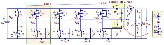
Figure 2.
Power circuit of ML converter.
The lossless model of the proposed converter is assumed to explain modes of operation. The inductors to are considered to be of the same inductance level. Switches to are controlled by the pulse of duty cycle , while switch is controlled by the pulse of duty cycle . The gate pulse of switch is displaced by time , where the time period is T. The value of the duty ratio is chosen in such a way that its addition is always less than unity, i.e., .
3. Continuous Conduction Mode
The suggested ML converter will function in three different ways. The voltage and current waveforms of reactive components and semiconductor devices are depicted in Figure 3.
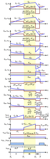
Figure 3.
Voltage and current typical waveforms in CCM.
3.1. MODE-I ( to )
Figure 4a illustrates the proposed ML converter circuitry for mode I. Switches S and to are switched on, while switch remains turned off. The input current is divided into parallel legs to charge inductors L and to , and capacitors to . At the same time, the input supply charges capacitor via diode and switch S. It is noteworthy that the diodes and D are reverse biased, and the diodes and to are forward biased. Additionally, all the passive components, i.e., inductors L and to , and and to are charged in parallel. The capacitor C supplies energy to the load R. The input voltage is applied across the inductors L, , , …, and , as well as the capacitors , , , …, and , during this mode. Therefore,
where is the average value of input voltage; , , , …, and are the average voltages across inductors L, , , …, and , respectively; , , , …, and are capacitors , , , …, and are average voltages, respectively. The current at the converter’s input and output terminals is given by
where and are instantaneous input and output currents, respectively; is the average output voltage; , , , …, and represent instantaneous currents flowing through inductors L, , , …, and , respectively; and instantaneous currents through capacitors C, , , , …, and are denoted by , , , , …, and , respectively. The current ripple via inductors L, , , …, and , i.e., , , , …, and , and voltage ripple across capacitors , , , …, and , i.e., , , …, and , can be expressed as
where f is the switching frequency of the converter.
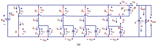
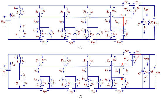
Figure 4.
Operating modes, (a) mode-I, (b) mode-II, and (c) mode-III.
The current through capacitors to and can be expressed as
where , , …, and are the current through capacitors and to .
3.2. MODE-II ( to )
Figure 4b illustrates the proposed ML converter circuitry for mode-II. Switches S and are turned off in this mode, whereas switch is turned on. During this mode, stored energy in the capacitors , , …, and , along with the input voltage, charges the inductors L, , …, and in series. The diodes D, , and to are not conducting due to reverse biasing, whereas the diodes are forward biased in this mode. Inductors L, to are charged and capacitors to are discharged. It is noteworthy to mention that the energy of capacitors and remains as it is, and capacitor C supplies power to load R. The summation of the and capacitors to voltages is reflected across the series connection of inductors L, , …, and . Therefore,
The current at the converter’s input and output is given by
The current ripple through inductors L, to and voltage ripple across capacitors to can be obtained as
The current through capacitors to and are as follows:
3.3. MODE-III ( to )
Figure 4c illustrates the proposed ML converter circuitry for mode-III. In this mode, switches S, , and are disabled. Inductors L, , …, and , as well as capacitors , , , …, and , are serially discharged with input voltage to supply power to load R and capacitor .
The diode D is forward biased, and reverse-biased diodes are , , , , …, . The voltage across load R is the sum of the voltages across the input , capacitors , to , and the inductors L, , to . Therefore,
The current at the converter’s input and output is given by
The current ripple through inductors L, to and voltage ripple across capacitors to can be obtained as
The current through capacitors to and is as follows:
4. Discontinuous Conduction Mode
The ML converter has four modes of operation. Figure 5 shows waveforms of reactive components and semiconductors.
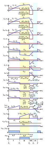
Figure 5.
Voltage and current typical waveforms in DCM.
4.1. MODE-I ( to )
This mode is similar to CCM mode-I. The currents via inductors L, , , …, and grow linearly, and their peak values are as follows:
where , , …, are the peak values of the current via inductors L, , …, , respectively, in mode-I. Upon the completion of the period (at ), all inductor currents attained the mode-I peak value. Therefore,
4.2. MODE-II ( to )
This mode is similar to CCM mode-II. The currents via inductors L, , , …, and grow linearly, and their peak values are as follows:
where , , …, are the peak values of the current via inductor L, , …, , respectively, in mode-II. At the completion of the period (at ), all inductor currents attained the mode-II peak value. Therefore,
4.3. MODE-III ( to )
This mode is similar to CCM mode-III. The currents via inductors L, , , …, and decrease linearly from their peak value and reach zero at the completion of this mode. The peak value of currents via inductors L, , , …, and in mode-III are calculated as follows:
where , , …, represent the maximum current values via inductors L, , …, and in mode-III, respectively. At , all the inductor currents reached zero levels.
4.4. MODE-IV ( to )
The suggested ML converter circuitry for mode-IV, i.e., DCM, is shown in Figure 6. Switches S, , and stay turned off, and the current in all inductors is zero. All the diodes are reverse biased, and the capacitor C supplies energy to the load R.
Figure 6.
ML converter in DCM.
The peak currents across all of the inductors in mode-II and -III are the same. As a result, by combining (15) and (17),
By solving (21), the value of is obtained as
The average capacitor C current is zero and can also be expressed as
Using (23), the ML converter’s DCM voltage gain is obtained as
where is normalized inductors time constant which is expressed as .
The boundary normalized inductor time constant is expressed as
Figure 7a,b shows the plot of versus duty cycle and for and 2, respectively; where the CCM and DCM areas are noticeable. The ML converter operates in CCM when is larger than . Additionally, to operate the ML converter in CCM, the conditions are as follows:
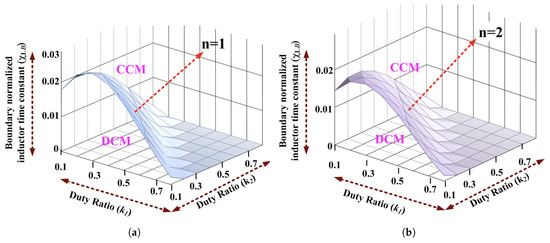
Figure 7.
Boundary for CCM and DCM, (a) , (b) .
5. Non-Ideal Model and Efficiency Analysis of ML Converter
The consideration is given to the existence of non-idealities and an illustration of the non-idealistic circuit of the ML converter is given in Figure 8. It is possible to illustrate the non-ideal properties of inductors by taking into account the resistance that is connected in series with each inductor. The non-ideal characteristics of switches are illustrated by considering on-state resistance in series with each switch. Due to the fact that diodes are not ideal, denotes their resistance, and denotes their threshold voltage. Consider , , and as voltage drops across resistances , , and , respectively.
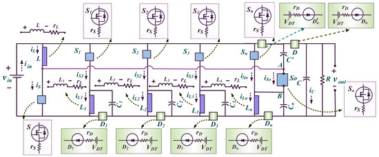
Figure 8.
ML converter with non-idealities.
5.1. MODE-I []
The inductors’ voltages can be found by
The capacitors’ C average voltage and current can be found by
5.2. MODE-II []
The inductors’ voltages can be found by
The capacitors’ C average voltage and current can be found by
5.3. State-III []
The inductors’ voltages can be found by
The capacitors’ C average voltage and current can be found by
By applying the capacitor-charged balanced principle on capacitor , the currents of inductors L, , , …, and are
The voltage gain with considering non-idealities is
where , , and . The total switching loss in power due switches can be found by
The total loss with considering switching rising and falling switches time can be obtained as
The power at the input side of the converter can be found by
The power at the output side of the converter can be found by . Using, (34)–(37), the efficiency of ML converter can be found by
where
From (39), when the non-ideality factors Y, and Z are reduced as well as when the ratio of switching loss to output power is lowered, the efficiency of the system improves. From (39) and (38), it is observed that higher efficiency can be obtained by selecting the appropriate duty cycle to achieve the desired voltage gain. The voltage drop is greater when the duty ratio of the converter is high. Moreover, the low value of the duty ratio and the higher value of the duty ratio result in low efficiency. Therefore, to achieve higher efficiency, it is suggested that the duty ratio should be high as compared to .
6. ML Converter with the Discrepancy in Inductors
The current and voltage characteristics of the ML converter are different than the ideal case when inductances L, to are not equal due to tolerances in the magnetic component. Additional operating modes will occur between actual mode-I and mode-II due to different currents in the inductors at the end of mode-I. These additional modes occur to make an equal current in the inductors since in mode-II, all the inductors are in series. It is noteworthy to mention that, for switching inductor-based circuitry, the current through inductors will be different, and some component voltages may be different than the ideal if unequal inductors are used [31,32,35]. The ratings of the components are based on the unequal inductances cases. There are many possible combinations of unequal inductances that occur in ML converters. The cases where and are considered to explain the operation of the ML converter with the discrepancy in the inductor. A similar analysis can be made for other cases and the additional intermediate molds depend on the number of unequal inductances. The inductor currents for the considered case are shown in Figure 9.
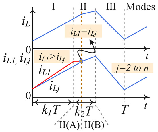
Figure 9.
Current waveforms through inductors when and .
6.1. MODE-I []
The switches S and to are switched on, while switch remains switched off. This mode equivalent circuitry is similar to the circuitry of CCM mode-I. The inductors’ voltages can be found by
The currents via inductors L, , , …, and grow linearly. However, since and , the current through inductors L, , …, and is low as compared to the current through inductor .
The voltages across switches are
The voltages across the diodes are
6.2. MODE-II(A) []
The switches S, and to are switched off, while switch is switched on. This is the additional mode that occurs due to the considered discrepancies in the inductors. The equivalent circuit is shown in Figure 10. The inductors’ voltages can be found by
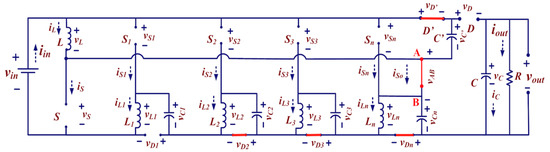
Figure 10.
Equivalent circuit of ML converter in mode II(A) when and .
The currents via inductors L, , …, and are the same and still grow linearly, and the current through is freewheel and constant.
The voltages across switches are
The voltages across diodes are
This mode will end when the currents through all the inductors become the same.
6.3. MODE-II(B) []
The switches S, and to are still switched off, while switches remain switched on. This mode is similar to CCM mode-II. The inductors’ voltages can be found by
At the end of this mode, the current through all the inductance reaches maximum value.
The voltages across switches are
The voltages across diodes are
6.4. MODE-III []
All the switches are switched off, and the equivalent circuitry is similar to CCM mode-III circuitry. The inductors’ voltages can be found by
At the end of this mode, the current through all the inductance reaches the minimum value.
The voltages across switches are
The voltages across diodes are
By using the inductor volt second balance principle, the voltage gain of the converter is calculated as
where and are the duty ratio for modes II(A) and II(B), respectively. We know . Therefore, the voltage gain is rewritten as,
The difference between the two inductor currents is due to the small practical difference in the inductance. Split mode-II into two sub-modes (mode-II(A) and -II(B)), and the current profiles of the inductors are different. However, finally, the voltage gain will be the same as (15). This is well known and also proved for other switched inductor-based circuitry; this was discussed by various authors in [31,32,35]. For the case where and , the voltage across diodes and switches is discussed above. However, for the other combination of discrepancy in inductors, the voltage across switches and diodes is different, and can be analyzed similarly as the above.
7. Design of ML Converter
For a specified voltage gain, the duty cycle can be determined as follows:
where is a function of duty cycles and , and it is obtained as
By using Equations (54) and (55), one can easily obtain the required duty cycle for the given voltage gain. For the purpose of design, the worst efficiency factor can be incorporated into the duty cycle calculation as the designed converter must also deliver the dissipated energy. Thus, while calculating the required duty cycle in Equation (56), we considered the worst-case scenarios of Equations (54) and (55) by adding the worst efficiency factor. This calculation method gives a more realistic duty cycle than just the equation without the efficiency factor. Therefore, the duty cycle parameters are designed with respect to the worst efficiency of the system as explained in [36]. The proposed system duty cycle while operating in is denoted by
The critical inductances of legs, i.e., , is calculated as
In this proposed system, the inductor current ripple, denoted by , is estimated to be 40% of the , where is the average current through inductor L. The critical current rating inductor, i.e., , is calculated as
The critical capacitances , , …, and are calculated as follows:
The critical voltage ratings of , , …, and capacitors are found as follows:
The critical voltage rating of capacitor , i.e., , is obtained as
The critical capacitance of the output capacitor , i.e., is obtained as
The relation between the input voltage and capacitor voltages can be obtained by
where is the equivalent of all the resistance present in the charging loop or path, which includes the on-state resistance of switches, forward resistance of the diode, and ESR of the switch. The switching spike across the capacitor occurs due to the difference between and , which can be minimized by selecting the appropriate device in the path, which has low internal resistance. For switches, the on-state resistance and the diode forward resistance should be minimal. This switching spike can also be reduced by selecting an appropriate capacitor with an accurate capacitance rating with low effective series resistance (ESR).
The critical voltages across the switches S, , , , … and , i.e., , , , , …, and , are
The critical voltages across the diodes D, ,, , …, and , i.e., , , , , …, and are
It is important that to design the converter, the ratings of all the components and semiconductor devices should be greater than the calculated critical value. Additionally, the on-state resistance of the switches, and forward resistance and the threshold voltage of the diode should be as minimal as possible.
8. Possible Control Schemes for the ML Converter
The converter derives its output voltage from the two duty ratios and . The plot of the voltage gain versus duty ratio for a different fixed values of duty ratio , versus duty ratio for different fixed value of duty ratio , and versus duty ratio and , is shown in Figure 11. The voltage gain depends on both duty ratios and , and the condition must be satisfactory to operate the converter. Therefore, both and are related to each other, and the desired voltage gain is possible to achieve in multiple ways by varying any one or both duty ratios.
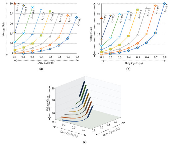
Figure 11.
Voltage gain (a) versus duty ratio for different fixed value of duty ratio , (b) versus duty ratio for different fixed value of duty ratio , and (c) versus duty ratio and .
Due to the benefits of the two duty ratios, there are three ways to manage the control functioning of the converter:
- Scheme-1: Fixed duty ratio and a adjust duty ratio ,
- Scheme-2: Fixed duty ratio and a adjust duty ratio ,
- Scheme-3: Adjust both duty ratios and .
8.1. Control Scheme-1
First, we fixed the duty ratio to achieve desired voltage gain based on the plot shown in Figure 11a. The value of duty ratio depends on the maximum and minimum values of the required voltage gain in the case of input voltage perturbation. For example, if the required minimum voltage gain (when input voltage is at maximum level) is 6.8, and the required maximum voltage gain (when the input voltage is at minimum level) is 26, then can be fixed at 0.4 and control from 0.1 to 0.5. Therefore, adjusting the duty ratio allows the output voltage to be controlled and maintained at a constant level whenever there is a change in the input voltage . Figure 12 illustrates the pulses that are associated with this method in which the duty ratio is adjusted by a value of in order to generate the suitable output voltage . The difference in input voltage determines the value of .
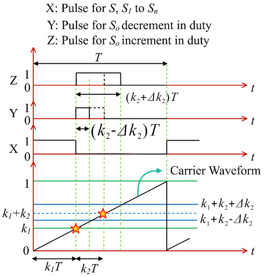
Figure 12.
Control scheme-1, (X: gate pulse for switches S, , Y: variation in the duty cycle of switch when voltage is increased at the input side, Z: variation in the duty cycle of switch when voltage is decreased at the input side).
8.2. Control Scheme-2
First, we fixed the duty ratio to achieve the desired voltage gain based on the plot shown in Figure 11b. The value of duty ratio depends on the maximum and minimum values of the required voltage gain in the case of input voltage perturbation. For example, if the required minimum voltage gain (when the input voltage is at a maximum level) is 5.5 and the required maximum voltage gain (when the input voltage is at minimum level) is 28, then can be fixed at 0.3 and control from 0.1 to 0.6. Therefore, adjusting the duty ratio allows the output voltage to be controlled and maintained at a constant level whenever there is a change in the input voltage . Figure 13 illustrates the pulses that are associated with this method, in which the duty ratio is adjusted by a value of in order to generate the suitable output voltage . The difference in input voltage determines the value of . Here, the duty ratio is shifted according to a change in the value of .
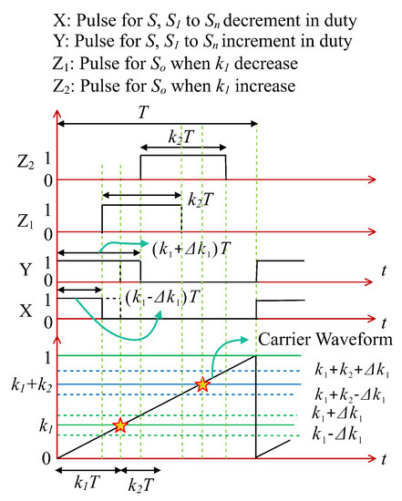
Figure 13.
Control scheme-2, (X: variation in the duty cycle of switches S, , when voltage is increased at the input side, Y: variation in the duty cycle of switches S, , when voltage is decreased at the input side, : the fixed duty cycle of switch is shifted when the voltage is increased at the input side, : the fixed duty cycle of switch is shifted when voltage is decreased at the input side).
8.3. Control Scheme-3
The desired voltage gain can be achieved by varying both duty ratios and based on the plot shown in Figure 11c and maintaining the condition . Therefore, when the input voltage changes, the duty ratios and are used to control and keep the output voltage steady. Figure 14 shows the pulses that are used in this method. The duty ratios and are changed by and to obtain the suitable output voltage . The values of and are determined by the change in . Both and duty ratio values changed and were dependent on one another during the disturbance.
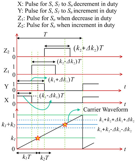
Figure 14.
Control scheme-3, (X: variation in the duty cycle of switches S, when voltage is increased at the input side, Y: variation in the duty cycle of switches S, when voltage is decreased at the input side, : the duty cycle of switch is shifted and varies when voltage is increased at the input side, : the fixed duty cycle of switch is shifted and varies when voltage is decreased at the input side).
9. Comparison of ML and Recent Converters
The findings of a comparison between the ML converter and other similar converters that were recently proposed are tabulated in Table 1. The novel converter developed in papers [31,32,33,34,35] is a variant on the simple boost converter. The converter is designed by adding one additional leg with voltage lift and active switched inductor techniques. The converter presented in [34,35] has the facility of choosing the number of legs, which is also one of the benefits of the proposed ML converter. One active switch is required to add one leg of the converter [34,35] and the proposed ML converter. However, the converter presented in the literature [35] requires five diodes and two inductors to design one leg of the converter, whereas the proposed ML converter requires only one inductor, one diode, and one capacitor to design one leg of the converter. Therefore, compared to [35], the proposed converter uses a smaller number of passive elements while designing the system. This results in the complexity of the converter being simplified, the overall cost of the system being reduced, and the converter being more compact. The ML converter shows an enormous increase in voltage gain when compared to [31,32,33,34]. The converter [33] and ML converter operates at two different duty cycles, allowing for greater variety in the duty cycle selection for the converter. This is the uniqueness of the ML converter. This characteristic of the ML converter permits two-duty cycle control, which is not achievable with ordinary single-switch converters. The switch-normalized voltage in the ML converter is lower than in the converters described in [33,34,35]. This enables the application of the ML converter using low-voltage rating devices. In the ML converter, an additional switch is employed to facilitate two different duty cycle operations of the converter. However, the switch voltage stress is less than the suggested converter’s output voltage. Additionally, the intermediate diodes utilized in this converter have a lower PIV rating than the converter’s output voltage. The PIV rating of the diodes decreases as the number of legs of the proposed converter increases. Therefore, diodes with lower PIV ratings than the output voltage are used to design the proposed converter system.

Table 1.
Comparison of converters.
10. Validation of the ML Converter
10.1. Equal Case of Inductances: Experimental Findings
The suggested converter behavior is examined experimentally, and the parameters are tabulated in Table 2. The prototype of the multi-leg (ML) converter with n = 2 is shown in Figure 15. The power density of the designed prototype is calculated as
where is the power density, is the output power, and is the product of the length, width, and height of the designed prototype.
Table 2.
Parameters of designed ML converter.
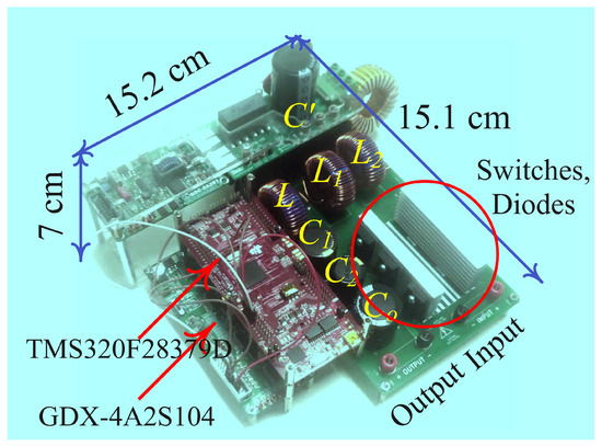
Figure 15.
Prototype of multi-leg (ML) converter with n = 2.
The voltage waveforms at the input and output are shown in Figure 16a. The output voltage of 399.8 V is achieved by supplying 36.3 V at the input voltage. It is tested that the suggested ML converter steps up the input voltage by a factor of 10. The experimental waveforms of the output voltage and output current are depicted in Figure 16b. It is perceived that the high gain converter delivers a voltage and current of 399.7 V and 1.25 A, respectively, at the output of the converter, which confirms the output power of 499.62 W. Figure 16c shows the input current and inductor L current waveforms. The average input current is 14.63 A, and the average current through inductor L is 4.77 A.
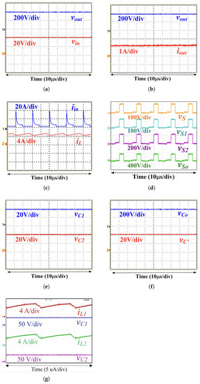
Figure 16.
Results, (a) and , (b) and , (c) and , (d) , , , and , (e) and , (f) and , (g) , , and .
The voltages across switches S, , , and are shown in Figure 16d. In mode-I, switches S, , and are all turned on, and the voltage across switch is −35.7 V. The switch is turned on in mode-II. It is observed that the switches S, , and are turned off, and the voltages across S, , and are 12.6 V, 12.5 V, and 25.5 V, respectively. All the switches are turned off in mode-III. It is observed that the voltages across S, , and and are 122.3 V, 122.1 V, 243.4 V, and 328.3 V, respectively. The voltages across capacitors and are shown in Figure 16e. The average voltages across the capacitor are 36.1 V and 35.8 V, respectively. The voltages of capacitors and are shown in Figure 16f. The average voltage of capacitor is 35.9 V and that of capacitor is 399.8 V. Figure 16g depicts the inductor and current and the capacitor and voltage waveform. The average currents through inductors and are 4.54 A and 4.63 A, respectively.
The proposed converter’s efficiency is measured at different output powers. Figure 17a shows a graph of efficiency versus load power. At a load power of 500 W, it can be seen that the prototype’s experimental efficiency is 93.61%. To analyze the discrepancies between theoretical and experimental efficiency, the plot of efficiency versus power is also drawn theoretically, as shown in Figure 17a. It is found that the theoretical efficiency of the converter is 94.2% at 500 W. Therefore, the differences between theoretical calculated efficiency and experimental efficiency are 0.47%. It is also found that the differences between theoretical calculated efficiency and experimental efficiency are almost consistent when the power is increased from 100 W to 500 W.
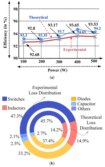
Figure 17.
Plots: (a) efficiency curve for different powers, (b) loss distribution when output power 500 W.
Figure 17b shows the loss distribution of the converter at a power of 500 W. It is found that switches cause 45.7% of the total losses in theory and 47.3% of the total losses in practice. It is also found that 37.4% of the total losses occur in the didoes in theory and 33.2% of the total losses occur in practice. It is observed that the switches experience maximum losses in the converter as compared to other devices. It is investigated that theoretically and experimentally, 16.9% and 17.4% losses occur, respectively, due to reactive components.
10.2. Discontinuous Conduction Mode Validation-Simulation Results
To investigate the performance of the ML converter in DCM, a simulation model is developed by considering three legs in the converter. To operate the converter in the DCM mode, the switching frequency is reduced to 25 kHz, all the inductor values are reduced to 325 H, and the converter is operated at low power by considering the load (R) value 1000 , and all of the capacitors’ value is 100 F. For the given specification, the normalized inductors’ time constant value for each inductor is calculated as . The expected voltage gain of the ML converter at duty ratios and is calculated by using (24) which is equal to 11.29. Figure 18a shows the obtained waveform of , , , and , where the input voltage is 40 V. It can be observed that the inductor L current is increased in mode-I and -II, decreased to zero in mode-III, and remains zero till the start of the next mode-I. The current ripple through inductor L is 8 A and the average current is 4.13 A. The average value obtained output voltage is 449.7 V and the output current is 1.12 A. The output voltage and current ripples are 3.1 V and 0.6 mA, respectively. Figure 18b shows the obtained waveform of , , , and , where the input voltage is kept constant at 40 V. It can be observed that the inductor current is increased in mode-I and -II, decreased to zero in mode-III, and remains zero till the start of the next mode-I. The current ripple through inductor L is 8 A, and the average current is 4.12 A, which is the same as the current through inductor L. The voltages across the switch in mode-II and -III are 10.2 V and 102.3 V, respectively. The voltages across the inductor in mode-I, -II, and -III are 40 V, 29.8 V, and −62.5 V, respectively. In DCM mode, the voltage across inductor drops to zero. All of the investigated values confirm the presented DCM theoretical analysis.
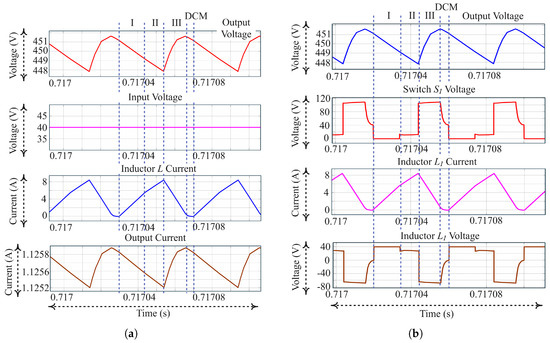
Figure 18.
Simulation results in DCM mode, (a) , , , and (b) , , , and .
10.3. Unequal Case of Inductances-Simulation Results
To investigate the performance of the ML converter with unequal inductances, a simulation model by considering and (70% discrepancy in inductance ) is developed, and the load (R) value of 320 is connected at the output. The performance is investigated at duty ratio and , with the switching frequency of 50 kHz. All the capacitors’ values are 100 F. Figure 19a shows the obtained waveform of , , , and , where the input voltage is 40 V. The average values of the output voltage and current are 400.2 V and 1.26 A. The average input current is 12.7 A. Figure 19b shows the obtained waveforms of , , , and . It can be observed that the currents through inductors L, , and are the same in each mode since . However, the current through inductor in mode-I is slightly greater than the current through inductor L due to . Mode-II is divided into sub-mode-II(A) and -II(B). In mode-II(A), the current of inductor holds a constant value, and this mode ends when the current through all of the inductors becomes equal. In mode- II(B) and -III, the currents through all the inductors are equal. It is observed that the peak-to-peak value of all the inductor currents is the same and equal to 0.6 A. However, the average current through inductor is higher than the average current through inductors L, , and since . Figure 19c shows the obtained waveform of , , , and . In mode-I, the average voltage across inductors L and is the same and equal to 40 V. In mode-II(A), the voltages across inductors L and are different and equal to 40 V and 0 V, respectively, which is expected due to . This unequal voltage across inductors results in unequal voltages across switches. The average voltage across switches S and are 0 V and 40 V. In mode-II(B), the average voltages across inductors L and are 33.2 V and 23.07 V, respectively, which is expected due to . The average voltages across switches S and are 6.9 V and 18.1 V in mode-II(B), respectively. In mode-III, the average voltages across inductors L and are −54.1 V and −38.8 V, respectively, which is expected due to . The average voltages across switches S and are 94.2 V and 78.8 V, respectively. All of the investigated values confirm the presented theoretical analysis for the unequal case of inductance.
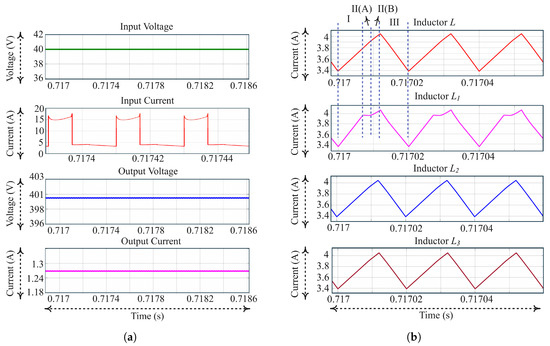
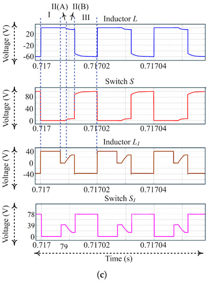
Figure 19.
Simulation results when and , (a) , , , and , (b) , , , and , (c) , , , and .
11. Conclusions
A novel DC–DC converter called the “multi-leg” (ML) converter is proposed to obtain a high voltage. The ML converter is designed by inserting multiple legs into a standard boost converter. Each leg is made up of a switch, an inductor, a diode, and a capacitor. The switches are turned on and off in such a way that the ML converter functions in three modes, and the output voltage is controlled through two duty cycles. As a result, the recommended converter allows for greater flexibility in selecting the duty cycle for switches. Other advantages of the ML converter include the following: (1) the size of inductors is less since following the principle of the switched inductor, (2) low current rating inductors, (3) less diodes than contemporary converters, (4) providing flexibility in the selection of legs, (5) low voltage rating devices, (6) low voltage rating capacitors in intermediate stages, (7) modular structure, etc. The converter operable in CCM and DCM operational analysis, design, and comparison is detailed and presented in this paper. The non-ideal model and various possible control schemes based on the selection of duty ratios to achieve constant voltage at the output are presented. Using an experimentally developed prototype, the performance of the ML converter for the equal inductances case is validated. Theoretically and experimentally, 16.9% and 17.4% losses, respectively, occur due to reactive components. At a load power of 500 W, the measured efficiency of the developed prototype is 93.53%. The DCM operation and unequal case of inductance are validated through a simulation model. Due to high voltage gain, unidirectional power flow, wide duty range operation, and flexibility in control and selection of duty ratio, the proposed converter is more suitable for 400 V DC microgrid PV applications. One of the SDG 7 objectives of the UN is a reliable, affordable energy system, which is supported by the suggested work targets. This effort promises to achieve SDG 12 by providing a high voltage gain converter system by employing a double-duty technique.
Author Contributions
Conceptualization, M.S.B.; methodology, M.S.B.; software, M.S.B.; validation, M.S.B. and D.A.; formal analysis, M.S.B.; investigation, M.S.B.; resources, M.S.B. and D.A.; data curation, M.S.B. and D.A.; writing—original draft preparation, M.S.B. and D.A.; writing—review and editing, M.S.B. and D.A.; visualization, M.S.B.; supervision, M.S.B. and D.A.; project administration, M.S.B. and D.A.; funding acquisition, M.S.B. and D.A. All authors have read and agreed to the published version of the manuscript.
Funding
This work was supported by research grants at Prince Sultan University; Saudi Arabia [SEED-2022-CE-103] and [SEED-2022-CE-95]. The authors would like to acknowledge the support of Prince Sultan University for paying the article processing charges (APC) of this publication.
Acknowledgments
All the other members from the Renewable Energy Lab (REL) at Prince Sultan University in Saudi Arabia provided technical help to the author.
Conflicts of Interest
The authors declare no conflict of interest.
References
- Qazi, A.; Hussain, F.; Rahim, N.A.; Hardaker, G.; Alghazzawi, D.; Shaban, K.; Haruna, K. Towards sustainable energy: A systematic review of renewable energy sources, technologies, and public opinions. IEEE Access 2019, 7, 63837–63851. [Google Scholar] [CrossRef]
- de Aguiar, C.R.; Fuzato, G.H.F.; Machado, R.Q.; Guerrero, J.M. An adaptive power sharing control for management of DC microgrids powered by fuel cell and storage system. IEEE Trans. Ind. Electron. 2019, 67, 3726–3735. [Google Scholar] [CrossRef]
- Hassan, W.; Lu, Y.; Farhangi, M.; Lu, D.D.C.; Xiao, W. Design, analysis and experimental verification of a high voltage gain and high-efficiency DC–DC converter for photovoltaic applications. IET Renew. Power Gener. 2020, 14, 1699–1709. [Google Scholar] [CrossRef]
- Xue, F.; Yu, R.; Huang, A.Q. A 98.3% efficient GaN isolated bidirectional DC–DC converter for DC microgrid energy storage system applications. IEEE Trans. Ind. Electron. 2017, 64, 9094–9103. [Google Scholar] [CrossRef]
- Afkar, M.; Gavagsaz-Ghoachani, R.; Phattanasak, M.; Martin, J.P.; Pierfederici, S. Proposed system based on a three-level boost converter to mitigate voltage imbalance in photovoltaic power generation systems. IEEE Trans. Power Electron. 2021, 37, 2264–2282. [Google Scholar] [CrossRef]
- Srinivasan, S.; Tiwari, R.; Krishnamoorthy, M.; Lalitha, M.P.; Raj, K.K. Neural network based MPPT control with reconfigured quadratic boost converter for fuel cell application. Int. J. Hydrog. Energy 2021, 46, 6709–6719. [Google Scholar] [CrossRef]
- Khan, S.; Mahmood, A.; Tariq, M.; Zaid, M.; Khan, I.; Rahman, S. Improved dual switch non-isolated high gain boost converter for DC microgrid application. In Proceedings of the 2021 IEEE Texas Power and Energy Conference (TPEC), College Station, TX, USA, 2–5 February 2021; pp. 1–6. [Google Scholar]
- Ramanathan, G.G.; Urasaki, N. Non-Isolated Interleaved Hybrid Boost Converter for Renewable Energy Applications. Energies 2022, 15, 610. [Google Scholar] [CrossRef]
- Salim, K.; Asif, M.; Ali, F.; Armghan, A.; Ullah, N.; Mohammad, A.S.; Al Ahmadi, A.A. Low-stress and optimum design of boost converter for renewable energy systems. Micromachines 2022, 13, 1085. [Google Scholar] [CrossRef] [PubMed]
- Zeng, Y.; Li, H.; Wang, W.; Zhang, B.; Zheng, T.Q. Cost-effective clamping capacitor boost converter with high voltage gain. IET Power Electron. 2020, 13, 1775–1786. [Google Scholar] [CrossRef]
- Yari, K.; Shahalami, S.H.; Mojallali, H. A novel nonisolated buck–boost converter with continuous input current and semiquadratic voltage gain. IEEE J. Emerg. Sel. Top. Power Electron. 2021, 9, 6124–6138. [Google Scholar] [CrossRef]
- Ahmed, H.Y.; Abdel-Rahim, O.; Ali, Z.M. New High-Gain Transformerless DC/DC Boost Converter System. Electronics 2022, 11, 734. [Google Scholar] [CrossRef]
- Jou, H.L.; Huang, J.J.; Wu, J.C.; Wu, K.D. Novel isolated multilevel DC–DC power converter. IEEE Trans. Power Electron. 2015, 31, 2690–2694. [Google Scholar] [CrossRef]
- Eskandarpour Azizkandi, M.; Sedaghati, F.; Shayeghi, H.; Blaabjerg, F. Two-and three-winding coupled-inductor-based high step-up DC–DC converters for sustainable energy applications. IET Power Electron. 2020, 13, 144–156. [Google Scholar] [CrossRef]
- Meng, T.; Yu, S.; Ben, H.; Wei, G. A family of multilevel passive clamp circuits with coupled inductor suitable for single-phase isolated full-bridge boost PFC converter. IEEE Trans. Power Electron. 2014, 29, 4348–4356. [Google Scholar] [CrossRef]
- Ragonese, E.; Spina, N.; Parisi, A.; Palmisano, G. An experimental comparison of galvanically isolated DC-DC converters: Isolation technology and integration approach. Electronics 2021, 10, 1186. [Google Scholar] [CrossRef]
- Zhao, Q.; Lee, F. High-efficiency, high step-up DC-DC converters. IEEE Trans. Power Electron. 2003, 18, 65–73. [Google Scholar] [CrossRef]
- Wu, T.; Lai, Y.; Hung, J.; Chen, Y. Boost converter with coupled inductors and buck–boost type of active clamp. IEEE Trans. Ind. Electron. 2008, 55, 154–162. [Google Scholar] [CrossRef]
- Wai, R.; Duan, R. High step-up converter with coupled-inductor. IEEE Trans. Power Electron. 2005, 20, 1025–1035. [Google Scholar] [CrossRef]
- Forouzesh, M.; Siwakoti, Y.; Gorji, S.; Blaabjerg, F.; Lehman, B. Step-up DC–DC converters: A comprehensive review of voltage-boosting techniques, topologies, and applications. IEEE Trans. Power Electron. 2017, 32, 9143–9178. [Google Scholar] [CrossRef]
- Guo, Z.; Li, H.; Liu, C.; Zhao, Y.; Su, W. Stability-improvement method of cascaded DC-DC converters with additional voltage-error mutual feedback control. Chin. J. Electr. Eng. 2019, 5, 63–71. [Google Scholar] [CrossRef]
- Mukherjee, N.; Strickland, D. Control of cascaded DC–DC converter-based hybrid battery energy storage systems—Part I: Stability issue. IEEE Trans. Ind. Electron. 2015, 63, 2340–2349. [Google Scholar] [CrossRef]
- Rosas-Caro, J.C.; Ramirez, J.M.; Peng, F.Z.; Valderrabano, A. A DC–DC multilevel boost converter. IET Power Electron. 2010, 3, 129–137. [Google Scholar] [CrossRef]
- Rajaei, A.; Shahparasti, M.; Nabinejad, A.; Niazi, Y.; Guerrero, J.M. Switching Strategy Development, Dynamic Model, and Small Signal Analysis of Current-Fed Cockcroft-Walton Voltage Multiplier. IEEE Open J. Power Electron. 2021, 2, 591–602. [Google Scholar] [CrossRef]
- Lei, Y.; Pilawa-Podgurski, R.C. Soft-charging operation of switched-capacitor DC-DC converters with an inductive load. In Proceedings of the 2014 IEEE Applied Power Electronics Conference and Exposition-APEC 2014, Fort Worth, TX, USA, 16–20 March 2014; pp. 2112–2119. [Google Scholar]
- Farswan, R.S.; Datta, A.; Kamble, G.; Fernandes, B. A low leakage transformer-less 3-level DC-DC boost converter for transformer-less PV inverters. In Proceedings of the 2015 17th European Conference on Power Electronics and Applications (EPE’15 ECCE-Europe), Geneva, Switzerland, 8–10 September 2015; pp. 1–10. [Google Scholar]
- Mayo-Maldonado, J.C.; Valdez-Resendiz, J.E.; Sanchez, V.M.; Rosas-Caro, J.C.; Claudio-Sanchez, A.; Puc, F.C. A novel PEMFC power conditioning system based on the interleaved high gain boost converter. Int. J. Hydrog. Energy 2019, 44, 12508–12514. [Google Scholar] [CrossRef]
- Baddipadiga, B.P.; Ferdowsi, M. A high-voltage-gain dc-dc converter based on modified dickson charge pump voltage multiplier. IEEE Trans. Power Electron. 2016, 32, 7707–7715. [Google Scholar] [CrossRef]
- Tewari, N.; Thazhathu, S.V. Family of modular, extendable and high gain dc–dc converter with switched inductor and switched capacitor cells. IET Power Electron. 2020, 13, 1321–1331. [Google Scholar] [CrossRef]
- Sadaf, S.; Bhaskar, M.S.; Meraj, M.; Iqbal, A.; Al-Emadi, N. A novel modified switched inductor boost converter with reduced switch voltage stress. IEEE Trans. Ind. Electron. 2020, 68, 1275–1289. [Google Scholar] [CrossRef]
- Yang, L.S.; Liang, T.J.; Chen, J.F. Transformerless DC–DC converters with high step-up voltage gain. IEEE Trans. Ind. Electron. 2009, 56, 3144–3152. [Google Scholar] [CrossRef]
- Bhaskar, M.S.; Alammari, R.; Meraj, M.; Padmanaban, S.; Iqbal, A. A new triple-switch-triple-mode high step-up converter with wide range of duty cycle for DC microgrid applications. IEEE Trans. Ind. Appl. 2019, 55, 7425–7441. [Google Scholar] [CrossRef]
- Lakshmi, M.; Hemamalini, S. Nonisolated high gain DC–DC converter for DC microgrids. IEEE Trans. Ind. Electron. 2017, 65, 1205–1212. [Google Scholar] [CrossRef]
- Maheri, H.M.; Babaei, E.; Sabahi, M.; Hosseini, S.H. High step-up DC–DC converter with minimum output voltage ripple. IEEE Trans. Ind. Electron. 2017, 64, 3568–3575. [Google Scholar] [CrossRef]
- Babaei, E.; Maheri, H.M.; Sabahi, M.; Hosseini, S.H. Extendable nonisolated high gain DC–DC converter based on active–passive inductor cells. IEEE Trans. Ind. Electron. 2018, 65, 9478–9487. [Google Scholar] [CrossRef]
- Hauke, B. Basic Calculation of a Boost Converter’s Power Stage; Application Report November; Texas Instruments: Dallas, TX, USA, 2009; pp. 1–9. [Google Scholar]
Publisher’s Note: MDPI stays neutral with regard to jurisdictional claims in published maps and institutional affiliations. |
© 2022 by the authors. Licensee MDPI, Basel, Switzerland. This article is an open access article distributed under the terms and conditions of the Creative Commons Attribution (CC BY) license (https://creativecommons.org/licenses/by/4.0/).