Abstract
A single-switch N-stage Z-network high-gain boost converter is proposed in this study, which can be applied in the field of chip etching for bias provision. The circuit topology, operation mode, voltage gain and the control strategy are analyzed. Thereafter, the steady-state performance of the circuit is analyzed with small signal stability modeling. A simulation model is built using Simulink and compared with the traditional quadratic circuit. Combined with the control strategy, the circuit can obtain better steady-state performance by controlling the number of working N-networks and adjusting the duty ratio in the case of high voltage, wide range of voltage output and dynamic voltage output. The simulation model and hardware prototype of the single-switch four-stage Z-network high-gain boost circuit are built and tested, which have verified the effectiveness of the proposed design.
MSC:
68Q06
1. Introduction
Dry etching is an important step in the chip manufacturing process. In the etching process, ion energy, ion angle and ion density play important roles in the etching rate, surface reaction and etching selectivity, respectively [1]. These ion characteristics are influenced by the voltage bias applied to the electrode where the silicon wafer is located [2]. The biasing sources directly or indirectly relate to a high-voltage DC power supply. So, how to generate the high-voltage DC power supply with simple structure, high efficiency and low cost deserves attention in the field of chip etching. The etching process [3,4,5,6,7,8] and biasing voltage are shown in Figure 1.
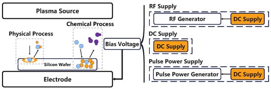
Figure 1.
Etching process and bias voltage.
In order to achieve the above high-voltage DC, many methods can be used [9]. Step-up DC–DC converters are one of most popular methods to directly pump up DC voltage. They can be divided into isolated boost circuits and non-isolated boost circuits. The isolated boost circuit is suitable for a situation requiring an isolated power supply [10,11,12], but the disadvantages are the large volume of the transformer and electromagnetic interference. Non-isolated boost circuits have many different structures, and the traditional boost circuit is one of the most popular boost cirucits with a simple structure. However, it has the drawback of a limited voltage gain. The rise of the duty ratio will lead to higher operating temperature of the switch, causing damage and failure of the switch.
In order to solve this problem, many high-gain boost circuits have been proposed [13,14]. For example, the cascade boost circuit [15] or the interleaved boost converter [16] are composed of multistage boost circuits, and the total gain is the product of the gain of each stage. However, it is difficult to control the circuit with multiple switches, and the cost is high. Some scholars put forward the quadratic boost circuit with a single switch [17,18], but the voltage stress of the switch is high, leading to a higher demand for the switching. Based on this quadratic boost circuit, the introduction of coupled inductor [19,20,21,22], switched inductor [23,24,25] and switched capacitor [26,27] have shown improvement of device stress or boost gain, but the circuit structure is complex, which is not conducive to the expansion of use. Some scholars put forward the quadratic boost circuit using a voltage doubler and voltage-lift technique to increase the voltage gain [28,29,30,31], but the introduction of voltage-double cells makes component design more complicated. The voltage gain, switch stress and diode stress in different methods are shown in Table 1.

Table 1.
The voltage gain, switch stress and diode stress in different Methods.
In this paper, a single-switch N-stage Z-network high-gain boost circuit (SS-NS-ZN-HGBC) is proposed. Inspired by the idea of Z-source structure [32,33,34,35,36] and quasi-Z-source structure [37,38,39], N-stage Z-network is introduced to achieve a high voltage gain while avoiding complex structures compared with other methods mentioned. Voltage gain can be greatly increased by increasing the number of Z-networks, which can be obtained with a small duty ratio. In addition, only one switch is used for control in the SS-NS-ZN-HGBC. Therefore, the control circuit will be simplified, and the control accuracy will be improved.
2. Modeling and Control Design of SS-NS-ZN-HGBC
2.1. Structure of the SS-NS-ZN-HGBC
The structure of the SS-NS-ZN-HGBC is shown in Figure 2. There is only one switch, and each dashed line frame represents a basic Z-network, which includes an inductor, a capacitor and two diodes. The operations of the SS-NS-ZN-HGBC contain two stages as follows.
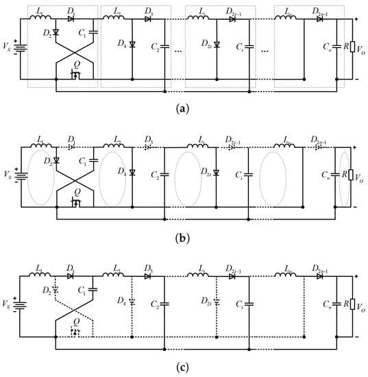
Figure 2.
The structure and operational model of the SS-NS-ZN-HGBC: (a) the structure of the SS-NS-ZN-HGBC; (b) stage I; (c) stage II.
Stage I: When Q is turned on, diodes , , …, are turned on, while diodes , , …, are turned off. For the first Z-network, the input voltage , inductor and diode are connected in series to form a closed loop, and provides power for this loop. For the other Z-networks, a capacitor from the upper Z-network , inductor and diode are connected in series to form a closed loop, and the capacitor provides power for the loop. In this case, the voltage of both ends of the inductor in the Z-network at all levels can be calculated.
Stage II: When Q is turned off, diodes , , …, are turned off, while diodes , , …, are turned on. For the first Z-network, the input voltage , inductor , diode and capacitor are connected in turn to form a closed loop. For the other Z-networks, an inductor , a diode , the capacitor in this Z-network and the capacitor from the upper Z-network are connected in turn to form a closed loop. In this case, the voltage of both ends of the inductor in the Z-network at all levels can be calculated.
For the inductor in the Z-network at all levels, in one period T, the voltage-second balance is used in (1) and (2).
The inductor has two working states, discontinuous current mode (DCM) and continuous current mode (CCM). In this paper, the inductors of the SS-NS-ZN-HGBC all work in CCM mode, so and are equal to the switch turning-on time and switch turning-off time . The and can be expressed with (4), where D is the duty cycle of the switch and can be adjusted by the control circuit, and T is the total time of the switching cycle.
Substituting (4) into (3), the gain of the circuit M can be as follows,
In addition, the voltage of each capacitor can be derived as below,
2.2. Parameter Design of Circuit Components
2.2.1. Inductors Design
In the SS-NS-ZN-HGBC, inductance has an important impact on the output voltage. To obtain the voltage gain M in (5), we must ensure that each inductor operates in the CCM mode, which means that the inductance of all inductors must be greater than critical inductance . Critical inductance is the minimum inductance to operate in the CCM mode. In CCM mode, the current through the inductor at any time must be greater than zero, so the minimum current is greater than zero.
According to the formula, , and is expressed in (8).
When the switch is turned on, the current through the inductor of each Z-network is shown in (9).
When the switch is turned off, the current through the inductor of each Z-network is shown in (10).
For the capacitor in the Z-network at all levels, in a period T, the ampere-second balance yields (1) and (2).
Therefore, the current flowing through the inductor can be calculated as follows,
In an ideal converter, the input power is equal to the output power ,
Substituting (5) into (13), we can calculate .
Substituting (14) into (12).
According to (15), should satisfy the following relation,
In addition, inductor decides whether the SS-NS-ZN-HGBC works in complete inductor supply mode (CISM). To work in CISM, the lowest current through should be greater than .
is the minimum inductance to let the SS-NS-ZN-HGBC work in CISM.
2.2.2. Output Capacitor Design
When the circuit operates in CISM mode, the ripple voltage of the output voltage is only related to the magnitude of the drop in the output capacitor during the conduction of the switch.
Term is introduced to represent the output voltage ripple rate and is expressed as follows.
The output capacitor is there determined by the output voltage ripple .
2.2.3. Forward Voltage Drop of Diode and DC Resistance of Inductor
The M in (5) is the value in an ideal case. In practice, the diode has a forward voltage drop when it is turned on, and the inductor has parasitic resistance, which reduces the voltage output of the system. Considering these factors, the inductors are re-analyzed as follows.
(24) can be expressed as,
can be calculated.
For a better description, we set the voltage output without considering the forward voltage drop of the diode and the DC resistance of the inductor as .
If the influence of forward voltage drop of the diode is not considered, (26) can be simplified as (29).
The influence of and on the output voltage will vary with the total number of Z-networks n, the order of Z-network i and the duty cycle ratioD. We express the influence of these factors in and for and , respectively.
Set D as a fixed value 0.35, and calculate and when , respectively. As shown in Figure 3, no matter what the value of n, and decrease as i increases. It means that the value of and has the greatest influence on the output voltage. To obtain higher output voltage, their values should reduce as much as possible. In addition, and increase as n increases, especially . It is an important reason why the actual voltage output of the high-order boost circuit is much less than the ideal voltage output.
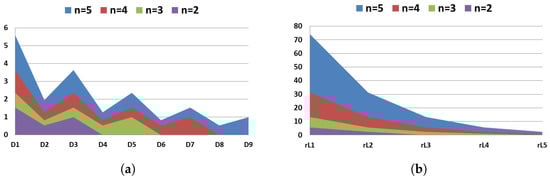
Figure 3.
The value of and when . (a) ; (b) .
The diode’s forward voltage drop has an inevitable impact on the output voltage. In order to reduce this impact, increasing the input voltage, selecting a lower positive voltage drop diode and reducing the duty cycle reasonably can be useful. As for DC resistance of inductors, selecting inductors with lower DC resistance or decreasing the value of load R can be helpful.
2.3. Control Design of the SS-NS-ZN-HGBC
First, the transfer function of the circuit with small signal analysis is derived, and then the compensation circuit is designed by observing the Bode diagram of the transfer function. The design process is shown in Figure 4.
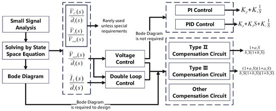
Figure 4.
Control design flow chart.
2.3.1. Small Signal Analysis
Through analyzing the stability of the Bode diagram of the transfer function, the appropriate control loop can be designed.
where is the duty ratio. Use the time average equivalence principle.
Superimpose the disturbance on the voltage and current parameters of (32) as follows.
Therefore, (32) can be expressed as follows,
Separate the DC part and the small-signal part as follows, (34).
To conduct steady-state analysis for the SS-NS-ZN-HGBC, the differential term of the DC part should be set as zero. In steady state, the relationship between different stages of voltage or current in N-stage can be calculated.
In the SS-NS-ZN-HGBC, when i is different, the values of , and are shown in Table 2.
Table 2.
The , and in the SS-NS-ZN-HGBC.
Perform Laplace transform on (38):
According to (40), the relationship between and or in a complex domain can be calculated.
According to (40), the relationship between and or in a complex domain can be calculated.
After calculation, the general form of is shown below.
The coefficients and can be calculated in MATLAB. Bode diagrams, concerning two-stage, three-stage, four-stage and five-stage Z-network high-gain boost circuits are plotted by MATLAB as shown in Figure 5.
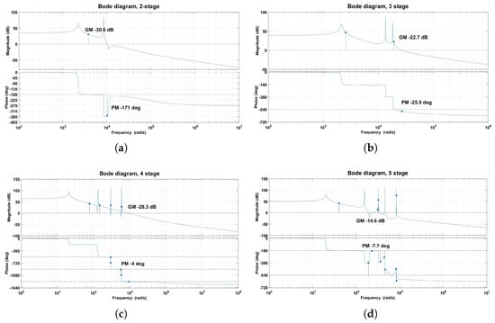
Figure 5.
Bode diagram of the single-switch N-stage Z-network high-gain boost converter: (a) 2-stage, GM −30.6 dB, PM −171 deg; (b) 3-stage, GM −22.7 dB, PM −25.9 deg; (c) 4-stage, GM −28.3 dB, PM −4 deg; (d) 5-stage, GM −14.6 dB, PM −7.7 deg.
It can be seen from the figures that as the number of Z-networks increases, the number of resonance peaks in an amplitude frequency characteristic diagram will also increase, but these resonance peaks are relatively concentrated, which lead a sharp phase drop in the phase-frequency characteristic figure.
2.3.2. Feedback Compensation Design
The appropriate compensation circuit can make the system more stable and reliable. Common compensation circuits, such as PI correction, PID control, double loop control and so on, all have their own advantages.
Without considering the current control, PI control is simple and efficient. It can basically achieve more accurate output, which shows in Figure 6. It processes the input signals actual output voltage and ideal output voltage , and then outputs the signal a, which adjusts the switching frequency of the switch transistor Q in order to minimize the difference between and .
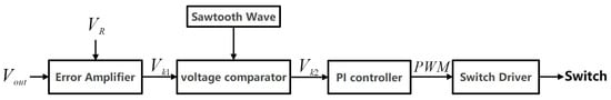
Figure 6.
Control design of duty ratio adjustment circuit.
The relationship between the output of the error amplifier and its input is shown in (44), where A is the amplification coefficient.
The relationship between the output of PI regulator and its input is shown in (45), where and are the coefficients depending on the circuit structure.
The voltage comparator compares with a sawtooth wave to output a PWM wave with an adjusted duty cycle. Then, this PWM wave controls the on and off switch through the switch transistor drive circuit to change the output voltage.
We perform small-signal analysis and Laplace transform on it in as follows.
The process of and sawtooth wave generating PWM through the comparator is expressed by in the transfer function, where is the peak value of the sawtooth wave. Therefore, the transfer function of this feedback compensation circuit can be expressed as follows,
After the compensation, the amplitude of the resonance peak becomes smaller, the amplitude margin and phase margin are sufficient and the system is stable. PI control can meet the requirements of stable operation of the system. For better steady-state performance, other more complex control circuits can be introduced, such as a single zero two-pole compensation circuit and a peak current compensation circuit [40].
3. Steady-State Performance Analysis
3.1. Analysis of Voltage Stress and Current Stress
When the switch is turned off, the voltage stress can be calculated.
When the switch is turned on, the current stress can be calculated.
Set D a fixed value of 0.35, and calculate and when . As shown in Figure 7a, we set a fixed value of 10 V to observe that , and have the first and second largest voltage stress, respectively. As shown in Figure 7b, we set a fixed value of 1 A to observe that , and have the largest current stress.
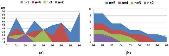
Figure 7.
The value of and when : (a) , V; (b) , A.
3.2. Analysis of Efficiency
3.2.1. The Power Loss of Inductor
Calculate the power loss of inductors .
Calculate total power loss of inductors .
3.2.2. The Power Loss of Capacitor
According to (9), (10) and (15), the current flowing through the capacitor in stage I and stage II is and separately.
T is the period of the switching transistor, and the power loss of the capacitor can be calculated.
Calculate the total power loss of capacitors .
3.2.3. Diode Conduction Loss
is the forward voltage drop of diode , and the current flowing through the diode can be approximated as the current of the inductor in (15). The diode conduction loss can be calculated.
Assuming that the same diodes are used in the circuit, the total diode conduction loss can be calculated.
3.2.4. Switch Conduction Loss
Here, is the resistance of the switch transistor, and is the current through it, so the switch transistor conduction loss is shown in (58)
3.2.5. Efficiency Analysis
Calculate the output power as follows,
Calculate the efficiency of the SS-NS-ZN-HGBC.
The ratio of power loss of different components to the total loss is shown in Figure 8.
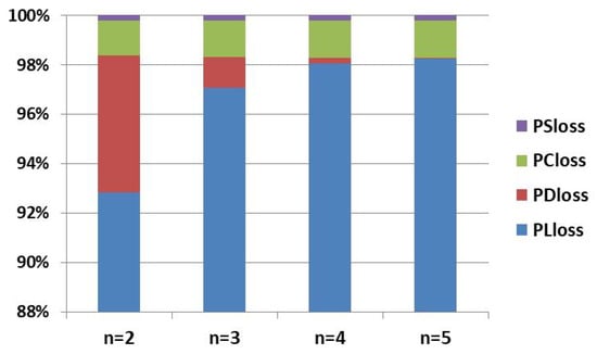
Figure 8.
The proportion of each part loss to total loss in different n.
The power loss of inductor accounts for the largest proportion of total loss, and the proportion will increase as n increases, while the proportion of diode conduction loss decreases as the n increases. and remain unchanged as the n increases.
4. Simulation Verification
4.1. Single-Switch Four-Stage Z-Network High Gain Boost Converter
A single-switch four-stage Z-network high-gain boost converter is taken as an example for simulation analysis, and its operational modes are shown in Figure 9.
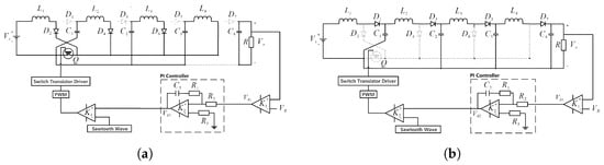
Figure 9.
Stage of the single-switch four-stage Z-network high-gain boost converter: (a) stage I; (b) stage II.
4.2. Simulation Studies and Result Analysis
According to Equations (20) and (21), the values of the circuit elements of a single-switch four-stage Z-network high-gain boost circuit can be calculated and are shown in Table 3.
Table 3.
Circuit parameters and number of components.
When the input voltage is 12 V, the duty cycle ratio is 0.35, and the switching frequency is 62,000 Hz, according to (62). The theoretical output voltage is 67.2 V. Considering the voltage drop of the diode and the resistance of the inductor, according to (62), the theoretical output voltage is 59.4 V.
PSIM is an electronic simulation software. We build and simulated a single-switch four-stage Z-network high-gain boost trcuit in PSIM, and the results are shown in Figure 10. The simulation result is consistent with the theoretical value.
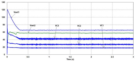
Figure 10.
Capacitor voltage output in PSIM.
According to (49) and (50), and have larger voltage stresses compared with other diodes theoretically, and has the largest current stress. The current and voltage waves of , and switch in PSIM are shown in Figure 11.
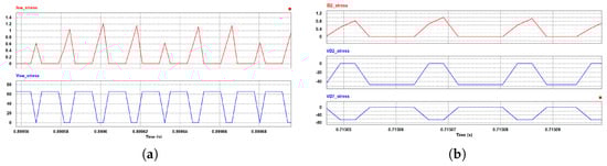
Figure 11.
The voltage stress and current stress of important components: (a) the stress waveforms of switch Q; (b) the stress waveforms of and .
5. Experimental Studies
To further verify the proposed method, an experimental prototype was built, and circuit parameters and the number of components are depicted in Table 4.
Table 4.
Circuit parameters and number of components.
The prototype consists of the SS-NS-ZN-HGBC, a PI control circuit, a DC power supply, a mobile charging power supply and a driver circuit. The control circuit is implemented in Arduino Uno. The experimental environment is shown in Figure 12.
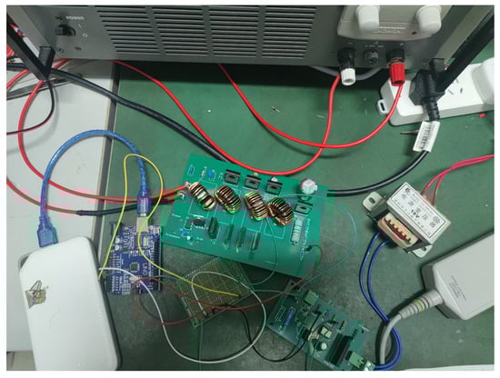
Figure 12.
Experimental environment.
The duty ratio D is 0.25, and the switching frequency f is 62,000 Hz. The Arduino Uno converts the input voltage (0–5 V) to the digital signal (0–255), and then outputs the PWM control signal after the PI control program proceeding. The and of the PI controller used in the experiment was 0.001 and 1.1, respectively. The experimental result waveforms are shown in Figure 13. The waveforms of the input voltage , output voltage and drive signal PWM in open loop are shown in Figure 13a. As shown in Figure 13b, in the experimental results, is close to the theoretical result of 12.64 V.
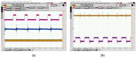
Figure 13.
Experimental result waveforms: (a) PWM, , in open loop; (b) output voltage with PI control.
Table 5 shows the output voltage in different methods when input voltage is 4 V and the duty ratio D is 0.25. The voltage gain M of the quadratic boost circuit with coupled inductors is related to its turns ratio N of the coupled inductors, which varies in different cases. This is not shown in Table 5.
Table 5.
Circuit parameters and number of components.
Compared with other methods, the SS-NS-ZN-HGBC has a much higher output voltage with the same input voltage and duty ratio because of its high voltage gain. The experimental results are consistent with the simulation results and theoretical analysis, which verify the effectiveness of the proposed design.
6. Conclusions
This study has proposed a class of general single-switch N-stage Z-network high-gain converters. Small signal modeling and stability analysis have been conducted for the converter. Simulations and prototype experiments were carried out on a 4-stage Z-network boost converter as an example, with a closed-loop control system. The simulation and experimental results agree well with the theoretical analysis, which verifies the effectiveness of the design approach. Compared with other methods mentioned, the SS-NS-ZN-HGBC has a higher voltage gain with a small duty ratio and only one switch. Its structure is simple and easy to expand.
Therefore, the proposed SS-NS-ZN-HGBC can be used for various applications that require high DC voltages, e.g., the etching process in chip manufacturing, auxiliary power supplies for electrical vehicles, and medical X-ray equipment. However, although the SS-NS-ZN-HGBC has a very high voltage gain, its voltage stress is also relatively high. In future research, some auxiliary circuits can be designed to reduce the voltage stress of the switch and diodes for wide practical applications.
Author Contributions
Conceptualization, G.Z.; software, X.L.; validation, W.L. (Weiqun Lin); formal analysis, X.L. and T.L.; writing—original draft, X.L; writing—review and editing, S.S.Y.; project administration, G.Z.; funding acquisition, W.L. (Weiping Le). All authors contributed equally to this work. All authors have read and agreed to the published version of the manuscript.
Funding
This research received no external funding.
Data Availability Statement
Not applicable.
Conflicts of Interest
The authors declare no conflict of interest.
References
- Dai, Z.; Mao, M.; Wang, Y. Physical Basis of Plasma Etching Process. Physics 2006, 35, 693–698. [Google Scholar]
- Liu, Z. Study on Ion energy and Angle Distribution on the Plate in Pulse Plasma Etching Process. Master’s Thesis, Dalian University of Technology, Dalian, China, 2016. [Google Scholar]
- Yan, X.; Jia, J. Study On Working Principle and Etching Performance of Focused Ion Beam. Equip. Electron. Prod. Manuf. 2010, 39, 14–16+32. [Google Scholar]
- Lai, W.; Liao, G.; Shi, T.; Yang, S. Study on Reactive Ion Etching Processing Technology. Semicond. Technol. 2006, 31, 414–417. [Google Scholar]
- Ren, Y. Present Situation and Future Development of Ion Etching Technology. Opt. Precis. Eng. 1998, 6, 8–15. [Google Scholar]
- Zhao, L.; Zhou, M.; Wang, S.; Li, J.; Huo, C.; Zhou, X. Ion Beam Etching. Semicond. Technol. 1999, 24, 39–42. [Google Scholar]
- Liu, Z. Plasma Etching. Chin. J. Nat. 1998, 20, 342–344. [Google Scholar]
- Guan, Y.; Lei, C.; Liang, T.; Bai, Y.; Qi, L.; Wu, X. Study On RIE Reactive Ion Etching Process of Silicon Nitride. Electron. Meas. Technol. 2021, 44, 107–112. [Google Scholar] [CrossRef]
- Zhang, G.; Chen, J.; Zhang, B.; Zhang, Y. A critical topology review of power electronic transformers: In view of efficiency. Chin. J. Electr. Eng. 2018, 4, 90–95. [Google Scholar] [CrossRef]
- Jiang, X. Research on Topology Theory and Control Technology of Isolated Full-Bridge DC-DC Boost Converter. Ph.D. Thesis, University of Chinese Academy of Sciences, Beijing, China, 2006. [Google Scholar]
- Anjel, J.; Gerald, C. Enhanced Isolated Boost DC–DC Converter with Reduced Number of Switches. In Proceedings of the International Conference on Artificial Intelligence, Smart Grid and Smart City Applications, Cairo, Egypt, 8–10 April 2020. [Google Scholar]
- Wang, Y.; Chen, S.Z.; Wang, Y.; Zhu, L.; Guan, Y.; Zhang, G.; Yang, L.; Zhang, Y. A Multiple Modular Isolated DC/DC Converter With Bidirectional Fault Handling and Efficient Energy Conversion for DC Distribution Network. IEEE Trans. Power Electron. 2020, 35, 11502–11517. [Google Scholar] [CrossRef]
- Zhang, G.; Wang, Z.; Yu, S.S.; Chen, S.Z.; Zhang, B.; Iu, H.H.C.; Zhang, Y. A Generalized Additional Voltage Pumping Solution for High-Step-Up Converters. IEEE Trans. Power Electron. 2019, 34, 6456–6467. [Google Scholar] [CrossRef]
- Zhang, G.; Yu, S.S.; Chen, W.; Zhang, B.; Zhang, Y. A General Polynomial Reverse Design of Step-Up Converters for EV Battery Applications. IEEE Trans. Veh. Technol. 2022, 71, 2628–2638. [Google Scholar] [CrossRef]
- Duan, W.; Wang, H. A Cascade High Gain DC / DC Boost Converter. Electr. Energy Manag. Technol. 2020, 7, 54–60. [Google Scholar] [CrossRef]
- Garrigós, A.; Marroquí, D.; García, A.; Blanes, J.M.; Gutiérrez, R. Interleaved, switched-inductor, multi-phase, multi-device DC/DC boost converter for non-isolated and high conversion ratio fuel cell applications. Int. J. Hydrogen Energy 2019, 44, 12783–12792. [Google Scholar]
- Yang, P. Research on Quadratic Boost Converter. Ph.D. Thesis, Southwest Jiaotong University, Chengdu, China, 2013. [Google Scholar]
- Ortiz-Lopez, M.G.; Leyva-Ramos, J.; Diaz-Saldierna, L.H.; Garcia-Ibarra, J.M.; Carbajal-Gutierrez, E.E. Current-Mode Control for a Quadratic Boost Converter with a Single Switch. In Proceedings of the IEEE Power Electronics Specialists Conference, Orlando, FL, USA, 17–21 June 2007. [Google Scholar]
- Cao, T.; Liu, W.; Guo, Y.; Chen, Z.; Wang, J.; Sun, Z.; You, F.; Luo, Q. Dual Coupled Inductor Quadratic High Gain DC-DC Converter. Trans. China Electrotech. Soc. 2015, 30, 104–112. [Google Scholar] [CrossRef]
- Cheng, S.; Zhao, S. Coupled Inductor High Gain DC-DC Converter with Dual Switch Quadratic Structure. J. Power Supply 2019, 19, 1366–1379. [Google Scholar]
- Axelrod, B.; Berkovich, Y. DC-DC converter based on the switched-coupled-inductor quadratic boost converter and diode-capacitor Dickson multiplier. In Proceedings of the 2017 19th European Conference on Power Electronics and Applications (EPE’17 ECCE Europe), Warsaw, Poland, 11–14 September 2017. [Google Scholar]
- Yang, F.; Ruan, X.; Wu, G.; Ye, Z. Discontinuous-Current Mode Operation of a Two-Phase Interleaved Boost DC–DC Converter with Coupled Inductor. IEEE Trans. Power Electron. 2017, 33, 188–198. [Google Scholar]
- Tang, J.; Shao, S.; Sun, T. Improved Quadratic Boost Circuit Based On Switched Inductor Network. China Strateg. Emerg. Ind. 2018, 2, 181–182. [Google Scholar] [CrossRef]
- Zhang, J.; Yang, Y.; Wang, D. Dynamic analysis and chaos control of the switched-inductor boost converter with the memristive load. Int. J. Circuit Theory Appl. 2021, 49, 2007–2020. [Google Scholar]
- Zhang, G.; Wang, Z.; Iu, H.H.C.; Chen, S.Z.; Ye, Y.; Zhang, B.; Zhang, Y. Unique Modular Structure of Multicell High-Boost Converters with Reduced Component Currents. IEEE Trans. Power Electron. 2018, 33, 7795–7804. [Google Scholar] [CrossRef]
- Zeng, Y.; Li, B.; Tang, L.; Ma, Z. Research On A Quadratic High Gain Boost Converter with Switched Capacitor. J. Power Supply 2018, 16, 8–13. [Google Scholar] [CrossRef]
- Wang, Z.; Zhang, G.; Chen, S.; Zhang, Y. Two Impedance-Network DC-DC Converters Based on Switched-Capacitor Techniques. In Proceedings of the 2018 IEEE International Power Electronics and Application Conference and Exposition (PEAC), Shenzhen, China, 4–7 November 2018; pp. 1–5. [Google Scholar] [CrossRef]
- Laha, A. A High Voltage Gain Quadratic Boost Converter using a Voltage Doubler and Voltage-Lift Technique. In Proceedings of the 2020 IEEE International Conference on Power Electronics, Smart Grid and Renewable Energy (PESGRE), Cochin, India, 2–4 January 2020. [Google Scholar]
- Yang, L.S.; Liang, T.J.; Lee, H.C.; Chen, J.F. Novel High Step-Up DC–DC Converter With Coupled-Inductor and Voltage-Doubler Circuits. IEEE Trans. Ind. Electron. 2010, 58, 4196–4206. [Google Scholar] [CrossRef]
- Zhu, M.; Luo, F.L. Series SEPIC implementing voltage-lift technique for DC-DC power conversion. IET Power Electron. 2008, 1, 109–121. [Google Scholar] [CrossRef]
- Prudente, M.; Pfitscher, L.L.; Emmendoerfer, G.; Romaneli, E.F.; Gules, R. Voltage Multiplier Cells Applied to Non-Isolated DC–DC Converters. IEEE Trans. Power Electron. 2008, 23, 871–887. [Google Scholar] [CrossRef]
- Wang, L.; Qian, Z.; Peng, F. Z-source Boost Converter. Electr. Drive 2006, 36, 28–29+32. [Google Scholar] [CrossRef]
- Peng, F.Z. Z-source inverter. IEEE Trans. Ind. Appl. 2003, 39, 504–510. [Google Scholar] [CrossRef]
- Mousavi, S.; Babaei, E. Single-Phase Dynamic Voltage Restorer Based on AC-AC Trans-Z-Source Converter for Voltage Sag and Swell Mitigation. In Proceedings of the 2021 12th Power Electronics, Drive Systems, and Technologies Conference (PEDSTC), Tabriz, Iran, 2–4 February 2021. [Google Scholar]
- Zhang, G.; Wu, Z.; Yu, S.S.; Trinh, H.; Zhang, Y. Four Novel Embedded Z-Source DC–DC Converters. IEEE Trans. Power Electron. 2022, 37, 607–616. [Google Scholar] [CrossRef]
- Zhang, G.; Li, Z.; Zhang, B.; Qiu, D.; Xiao, W.; Halang, W.A. A Z-Source Half-Bridge Converter. IEEE Trans. Ind. Electron. 2014, 61, 1269–1279. [Google Scholar] [CrossRef]
- Zhao, Y. Topology Research Based on Quasi-z-Source DC-DC Converter. Master’s Thesis, Shandong University of Science and Technology, Qingdao, China, 2018. [Google Scholar] [CrossRef]
- Yun, Z.; Shi, J.; Lei, Z.; Jing, L.; Sumner, M.; Ping, W.; Xia, C. Wide Input-Voltage Range Boost Three-Level DC–DC Converter with Quasi-Z Source for Fuel Cell Vehicles. IEEE Trans. Power Electron. 2017, 32, 6728–6738. [Google Scholar]
- Ayad, A.; Karamanakos, P.; Kennel, R. Direct Model Predictive Current Control Strategy of Quasi-Z-Source Inverters. IEEE Trans. Power Electron. 2016, 32, 5786–5801. [Google Scholar] [CrossRef]
- Yang, P.; Xu, J.; Zhang, S.; Wang, J. Quadratic Boost Converter Controlled By Peak Current. Trans. China Electrotech. Soc. 2011, 26, 101–107. [Google Scholar] [CrossRef]
Publisher’s Note: MDPI stays neutral with regard to jurisdictional claims in published maps and institutional affiliations. |
© 2022 by the authors. Licensee MDPI, Basel, Switzerland. This article is an open access article distributed under the terms and conditions of the Creative Commons Attribution (CC BY) license (https://creativecommons.org/licenses/by/4.0/).