Abstract
Metal-coated mesoporous PSi (mesoPSi) opens up disruptive perspectives for biosensing, which is primarily enabled by surface-enhanced Raman scattering (SERS). Although the unique performance of SERS-active substrates based on metal-coated mesoPSi has already been praised, influence of defects in silicon wafer on its morphology has not been revealed. Defects lead to formation of spiral regions in mesoPSi with varying porosity, which affects SERS activity of the overlying metallic nanostructures. It limits the reliability of SERS analysis. Here, we investigate repeatability of morphology and SERS activity of silver particles on mesoPSi as a function of defects in parent silicon, which are induced by irregular dopant levels. We propose an original corrosion approach that has not yet been applied to control the morphology of silicon nanostructures in general and mesoPSi in particular. By replacing silicon nanocrystallites with sacrificial copper nanoparticles, we were able to eliminate the surface irreproducibility of mesoPSi. The copper-corrosion-modified porous silicon surface was shown to be a suitable substrate for reliable SERS-active substrates. In more detail, SERS-active substrate based on mesoPSi without a defective surface layer allowed for a more than 40% increase in the SERS-active surface area with a signal deviation of only 10 % compared to that with a defective layer.
1. Introduction
Porous silicon (PSi) is an artificially formed nanomaterial consisting of a highly developed network of pores within a bulk silicon wafer [1]. Since its discovery in 1956 [2], PSi has undergone significant evolution—from use as isolating areas [3,4] and sacrificial layers for layer transfer technology [5] in microelectronics and microelectromechanical systems, to applications in lithium-ion battery anodes [6], integrated waveguides in optoelectronics [7,8], luminescent agents in sensing [9,10], tissue engineering [11], and drug delivery systems in biomedicine [12,13]. PSi layers are typically fabricated by electrochemical/chemical etching of silicon wafers in solutions based on hydrofluoric acid [14,15,16,17,18]. They exhibit a wide range of unique properties not observed in bulk silicon, including but not limited to photo- and electroluminescence [19,20], extremely developed surface area, biocompatibility [21], and biodegradability [22,23]. The structural parameters of PSi, such as porosity, pore diameter, and the spacing between pore centers, can be precisely controlled through the etching conditions and the type of silicon wafer used [24]. This makes PSi an excellent “host” platform for the controlled incorporation of “guest” nanostructures made from various materials (e.g., metals), with precise control over their size, shape, and spatial location. This capability has enabled the widespread use of PSi for nanoscale fabrication of ordered arrays and ensembles with defined morphological and electrodynamic properties [25,26,27,28]. For example, it has been used to fabricate plasmonic substrates that possess antibacterial properties [29,30] and activity in surface-enhanced Raman scattering (SERS) spectroscopy, including metallic nanoparticles [31], polydisperse particles [32], dendrites [33], and nanovoids [34].
According to IUPAC classification, PSi is divided into three categories based on pore diameter: microporous (pore diameter < 2 nm), mesoporous (2–50 nm), and macroporous (>50 nm) silicon [35,36,37]. Although SERS-active nanostructures can be fabricated using the three types [38], the strongest Raman signal enhancements are typically obtained with metal-coated mesoporous silicon (mesoPSi) formed by electrochemical etching. A remarkable detection limit down to the single-molecule level has already been demonstrated for both small molecules [39,40] and macromolecules [41]. Thanks to the exceptional SERS efficiency and a simple, cost-effective fabrication process—requiring only two wet Si-compatible steps—metal-coated mesoPSi substrates have the potential to become strong contenders in the SERS platform market. However, a significant challenge must be addressed before they can be widely adopted. An effective SERS-active substrate must be stable, offer a high enhancement factor, and provide reproducible SERS signals [42]. While the first two criteria are commonly met by mesoPSi-based substrates, signal reproducibility remains their “Achilles’ heel”. This issue mainly stems from defects in the parent silicon used to fabricate mesoPSi. These defects originate from irregular dopant concentration distributions in monocrystalline Si ingots grown by the Czochralski method. It should be noted that this feature is characteristic of mesoPSi formed on heavily doped wafers of electron conductivity at high current densities as reported elsewhere [43,44]. Although such inhomogeneities are not critical in microelectronics, where only surface layers are typically used, they become problematic when deeper regions of the wafer are processed, as in mesoPSi fabrication. The vertical alignment of the mesopore array is disrupted, leading to irregularities in the final metallic nanostructure. Since the morphology of the plasmonic metal directly influences the Raman signal enhancement, these structural inconsistencies drastically affect the SERS response of PSi-based substrates. Such defects are often visible to the naked eye as alternating dark and light circular stripes within the PSi layer [45]. When silver nanostructures are fabricated in these areas, a significant variation in SERS signal intensity is typically observed. An approach to improving the structural uniformity of PSi—and therefore the consistency of the resulting ‘guest’ nanostructures—involves the implantation of ions prior to electrochemical etching of the n+-type silicon wafer. This method has enabled the formation of mesoPSi with a more homogeneous dopant distribution in the surface layer, resulting in approximately a 5% reduction in spot-to-spot SERS signal variation in the final PSi-based plasmonic nanostructure. However, this technique is not easily integrated into standard metal-coated PSi fabrication protocols. Moreover, implementing it would compromise the key advantages of PSi templates: their simplicity and low cost. To maintain the high market potential of SERS-active substrates based on PSi, more accessible and scalable solutions must be developed.
To address this issue, we propose a robust method for producing mesoPSi layers with highly uniform pore opening sizes (surface porosity), based on a simple corrosive metal deposition and etching process. By combining this approach with the fabrication of plasmonic silver nanostructures, we demonstrate significant improvements in spot-to-spot SERS signal intensity reproducibility along with enhanced Raman signal intensity. The developed technique offers a rapid, user-friendly, and cost-effective means of controlling the structural, morphological, and optical properties of various nanostructures fabricated using mesoPSi templates.
2. Materials and Methods
2.1. Materials
A monocrystalline antimony-doped silicon wafer with (100) crystal orientation and a resistivity of 0.01 Ohm·cm (n+-Si) was purchased from the Kamerton branch of JSC ‘Integral’ (Pinsk, Belarus). Chemically pure isopropyl alcohol (C3H8O), analytical-grade copper sulfate (CuSO4·5H2O), 95–98% sulfuric acid (H2SO4), 70% nitric acid (HNO3), and 50% hydrogen peroxide (H2O2) were obtained from LLC ‘Khim-Analit’ (Minsk, Belarus). Technical-grade ethyl alcohol (C2H5OH) was provided by JSC ‘Belkhim’ (Minsk, Belarus), and 45% hydrofluoric acid (HF) was purchased from LLC ‘Mercury’ (Minsk, Belarus). Silver nitrate (AgNO3) and rhodamine 6G (R6G) were purchased from Sigma-Aldrich Chemie GmbH (Taufkirchen, Germany). All reagents were used without further purification. Deionized water was produced using a Milli-Q Ultrapure Water System (Merck Millipore, Darmstadt, Germany). A piranha solution was prepared by mixing H2SO4 and H2O2 in a 3:1 volume ratio. H2O2 for the piranha solution was diluted with DI water to 20%.
2.2. Fabrication of Mesoporous Silicon
First, the silicon wafer was diced into the 3 × 3 cm2 samples. Each Si sample was thoroughly cleaned by immersion in a freshly prepared piranha solution for 10 min under ambient conditions, followed by etching of the native SiO2 layer in HF diluted with DI water to 4.5%. Next, a mesoPSi layer was formed by electrochemical anodization of the cleaned wafer in an etching electrolyte composed of 45% HF, isopropyl alcohol (as a wetting agent) and water, mixed in a volume ratio of 1:1:3. Anodization was performed at a current density of 100 mA/cm2 for 45 s, using the Autolab PGSTAT302N potentiostat/galvanostat. Finally, the sample was rinsed with DI water and spin-dried. Schematic representation of the mesoPSi fabrication steps is shown in Figure 1a–c.
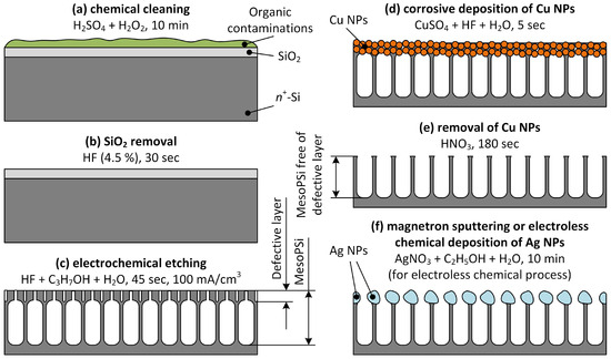
Figure 1.
Schematic representation of the experimental sample fabrication: (a) removal of organic contaminations, (b) removal of native SiO2, (c) formation of mesoPSi, (d) substitution of defective layer of mesoPSi with Cu NPs, (e) removal of Cu NPs with the rests of the defective layer, and (f) deposition of Ag NPs.
2.3. Removal of the Defective Surface Layer from Mesoporous Silicon
The surface layer was removed via corrosive copper deposition on the silicon skeleton of the mesoPSi sample, followed by etching in HNO3 diluted with DI water to 7%. The electrolyte for copper deposition was prepared by mixing a 0.25 M aqueous solution of CuSO4·5H2O with 45% HF in a volume ratio of 100:1. The mesoPSi sample was immersed in this electrolyte for 5 s, leading to the formation of copper nanoparticles (NPs) within the bottleneck layer, accompanied by partial dissolution of the silicon skeleton. Immediately afterward, the mesoPSi sample was placed in the diluted HNO3 solution for 180 s to etch away the Cu NPs. The sample was then rinsed with DI water and spin-dried. As a result, the mesoPSi sample free of the surface layer was obtained. A schematic representation of the defective layer removal is shown in Figure 1d,e.
2.4. Deposition of Silver on Mesoporous Silicon
Ag NPs were grown on the mesoPSi samples—with and free of the surface layer—using magnetron sputtering and electroless deposition techniques. Magnetron sputtering was performed using a MARS-100 (BSUIR, Minsk, Belarus) series system to form a 50-nm-thick film composed of Ag NPs. The film thickness was monitored using a quartz crystal sensor OI-001 (BSUIR, Minsk, Belarus). For electroless silver deposition, the mesoPSi sample was immersed in a 3 mM aqueous-ethanolic solution of silver nitrate (AgNO3) for 10 min as shown in Figure 1f. After deposition, the sample was rinsed with deionized water and spin-dried.
2.5. Characterization
The structural characterization of the experimental samples was carried out using a Hitachi S-4800 (Tokyo, Japan) scanning electron microscope (SEM), which offers a resolution of 1 nm. Elemental composition analysis was performed with a Stereoscan-360 SEM (Cambridge instruments, London, UK) equipped with a QUANTAX energy-dispersive X-ray (EDX) analyzer (Bruker Analytical, Berlin, Germany). The diameter of the focused electron beam was approximately 2 µm, and the depth of the analysis did not exceed 1 µm. The phase composition of the samples was investigated using a DRON-3M X-ray diffractometer (JSC Innovation Center "Burevestnik", St. Petersburg, Russia) with CuK radiation ( = 0.15406 nm) at room temperature, employing an exposure time of 4 s and a step size of 0.02°.
To quantitatively evaluate the surface uniformity achieved through our approach, we compared the porosity of mesoPSi before and after removal of the defective surface layer using both gravimetric and SEM image analysis methods. The gravimetric method involved measuring the sample mass before (m1) and after (m2) mesoPSi fabrication. Knowing the anodization surface area (SPSi), silicon density (Si, 2.32 g·cm [46]), and the thickness of the mesoPSi layer (dPsi), the porosity (p) was calculated using the following equation:
Porosity was also estimated via SEM image analysis, in which the cumulative surface area of visible pore openings in the top-view SEM images was calculated and divided by the total mesoPSi surface area captured in the image.
The organic dye R6G was used as an analyte for SERS measurements. The R6G powder was dissolved in DI water to prepare a basic solution with a concentration of 10 M, which was then diluted with water to obtain DI solutions down to a concentration of 10 M.
Silver-coated mesoPSi samples were immersed in 1 mL of the analyte solution for 1 h before SERS measurements, followed by a 30-s rinse in DI water to remove excess R6G molecules. SERS spectra were recorded using a 3D scanning confocal Raman microscope-spectrometer Confotec NR500 (SOL Instruments LLC, Minsk, Belarus). A laser with a wavelength of 473 nm was used for excitation. The initial laser power of 25 mW was attenuated to 1.3 mW after passing through the optical-mechanical unit and a 100× objective. SERS mapping was performed over a 48 × 48 µm2 area, corresponding to a 15 × 15 point grid.
2.6. Numerical Simulations
Electric field simulations were conducted for the silver-coated mesoPSi sample after removal of the defective surface layer, using the AC/DC module of the COMSOL Multiphysics software (v. 5.3) [47]. A finite element method was used to solve the 3D frequency-domain wave equation for the electric field, enabling the determination of its magnitude and spatial distribution. Floquet boundary conditions were applied to each facet of the pores in the model system. In the full-field formulation, the excitation source was a y-polarized plane wave with normal incidence, with a wavelength of 473 nm and propagation along the negative z-direction. The power of the excitation source was set to 1.3 mW.
3. Results and Discussion
3.1. Structural Parameters of Mesoporous Silicon Before and After the Defective Surface Layer Removal
For the study of structural parameters, SEM images of the mesoPSi surface were acquired at various magnifications before and after removal of the defective surface layer. Figure 2a,b show top-view SEM images of the freshly prepared mesoPSi surface, which exhibits periodic light and dark stripes following the irregular dopant distribution on the highly doped n+-Si wafer. These stripes correspond to regions with varying surface porosity in the mesoPSi layer. As seen in Figure 2a, the alternating light and dark stripes are 10–50 µm wide. A closer inspection of the boundary between the stripes in Figure 2b reveals a denser pore distribution in the dark one. The insets in Figure 2b show a wide variety of pore sizes and grayscale contrasts, with darker regions generally indicating deeper pores. As the doping level increases from 1018 to 1020 cm typical for the n+-Si wafers [48], the number of pores increases while the distance between them and the diameters of the pores are reduced. In the more doped area of the Si wafer, a greater number of antimony atoms segregate on its surface compared to the less doped area, which leads to the formation of an electron-depleted layer in the first seconds of the voltage biasing [49]. At the moment of breaking this layer, ordered pores start growing under it. However, the layer itself is no longer etched, and during further SEM analysis, it is strongly charged, resulting in the observation of a lighter region. Figure 2c presents a cross-sectional SEM image of the same mesoPSi sample, revealing morphology variations along the pore channels. In more detail, the pore entrances in the surface layer of mesoPSi form so-called bottlenecks. Bottleneck pores contribute to a broad distribution of pore entrance sizes. In addition to bottlenecks, numerous short collapsed ‘dead’ pores are also observed. Notably, the structural irregularities (bottlenecks and ‘dead’ pores) are confined to a thin surface layer of approximately 150 nm thickness. Once the mesoPSi layer becomes thicker, i.e., in the later stages of anodization, when the current density stabilizes across the sample surface, pores have rather uniform diameter and length. Although a deeper discussion of the mechanisms of pore formation in the thin Si surface layer is beyond the scope of this manuscript, those interested may find the more in-depth information elsewhere [50,51]. In contrast, the mesoPSi surface treated with the copper-assisted silicon corrosion method does not show a macroscopic stripe pattern, as illustrated in Figure 2d,e. The corresponding cross-sectional SEM image shown in Figure 2f confirms the absence of both ‘dead’ pores and bottlenecks, demonstrating the effectiveness of the proposed method in producing mesoPSi layers with homogeneous pore sizes.
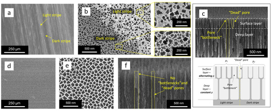
Figure 2.
SEM images of mesoPSi: (a,b) top-views at different magnifications and (c) cross-sectional view with corresponding schematic representation of pores arrangement (shown below) before removal of the mesoPSi defective surface layer, (d,e) top-views and (f) cross-sectional view after removal of the mesoPSi defective surface layer. The light (more doped) and dark (less doped) stripes observed in the freshly prepared mesoPSi (a–c) are caused by variation in porosity, which results from the irregular dopant distribution in the parent Si wafer. The dash yellow line shows pore boundaries.
Upon closer gravimetric and SEM image analysis, the pore distribution is found to be uniform in terms of density, size, and grayscale throughout the 3 cm2 surface area. Table 1 presents the gravimetrically determined mesoPSi porosities for the seven samples investigated in this work, before and after the copper-assisted corrosion. In addition, the surface porosity was calculated from the top-view SEM image of the sample. As shown in Table 1, the gravimetrically measured porosity values exhibit only a slight increase after removal of the mesoPSi surface layer. However, the variation in porosity from sample to sample is significantly reduced, from 5% for freshly prepared mesoPSi to 2% after copper-assisted corrosion. This change in absolute porosity is attributed to the nonspecific nature of the gravimetric method, which reflects an average total porosity encompassing both light and dark surface stripes as well as the bulk mesoPSi layer. In contrast, the SEM image analysis evaluates only the surface porosity and, therefore, reveals a dependence on the selected surface region, consistent with the observed differences between light and dark stripes in the freshly prepared mesoPSi. Notably, the porosity values obtained by both methods are nearly identical after removal of the surface layer. This outcome confirms the effectiveness of our method in eliminating the mesoPSi surface irregularities and exposing a homogeneous pore network.

Table 1.
Porosity of Samples Analyzed by Gravimetric and SEM Image Analysis Methods. A gravimetric porosity uncertainty is ±0.2%. An uncertainty of the porosity evaluated from the SEM images is ±0.8%.
3.2. Principle of the Copper-Assisted Corrosion for Removal of the Defective Surface Layer from Mesoporous Silicon
The study of the structural parameters of mesoPSi facilitated understanding the mechanism of removal of the defective surface layer of mesoPSi by the copper-assisted corrosion method.
Due to irregular pore morphology, it is challenging to precisely control the geometry of the ‘guest’ nanostructures, in our case, silver NPs. As a result, the localized surface plasmon resonance, whose spectral position is highly dependent on the nanoparticle size and shape, varies significantly across the mesoPSi surface. This variation is undesirable for the development of reliable and efficient SERS-active substrates, as it limits the substrate application when a specific excitation wavelength is required. The problem is further compounded by the wide distribution of interparticle distances, which leads to fluctuations in the sizes of the nanoscale gaps between metallic NPs, or ‘hot spots’, where the electromagnetic field is enhanced. This, in turn, causes substantial spot-to-spot variability in the SERS signal intensity.
To overcome these challenges, increasing the uniformity of the mesoPSi surface prior to nanostructure fabrication is essential. In this subsection, we describe the principle of our simple, cost-effective, and rapid method to remove the defective surface layer of mesoPSi, which reveals a uniform pore network for the subsequent formation of Ag NPs. The process begins with the standard fabrication of a mesoPSi layer, which is schematically shown in Figure 3a. Corrosive copper deposition is then performed using a solution of copper sulfate and diluted hydrofluoric acid. In this way, copper atoms partially replace silicon in the defective surface layer via chemical reactions, forming Cu NPs, as schematically depicted in Figure 3b. The duration of Cu deposition was adjusted to allow for the penetration of Cu NPs precisely into the defective surface layer, as follows from the SEM image in Figure 3c. XRD pattern shown in the inset of Figure 3c revealed prevalent orientations (111) and (100) of Cu nanocrystals. The mechanism of substitution of silicon and PSi with Cu NPs has been reported elsewhere [52,53]. Next, Cu NPs are removed by chemical etching in diluted HNO3, which also leads to destruction of the defective surface layer. This procedure exposes the deeper and more uniform layer of mesoPSi, as illustrated in Figure 3d.
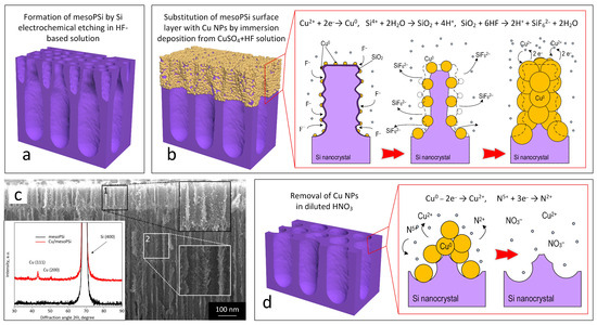
Figure 3.
Principle of the Cu-assisted corrosion for removal of the defective surface layer from mesoPSi: (a) schematic representation of freshly prepared mesoPSi, (b) schematic representation of substitution of the mesoPSi surface layer with Cu NPs including illustration of the corrosive Cu deposition chemical reactions following the addition of CuSO4 and HF (right image), (c) cross-section SEM image of mesoPSi after Cu deposition with magnified areas of (1) the defective surface layer coated with Cu NPs and (2) the deep porous layer free of Cu NPs; the inset shows XRD patterns of mesoPSi after Cu deposition (red curve) and following etching in the diluted HNO3 (black curve), and (d) schematic representation of chemical etching of Cu NPs with illustration of the chemical reactions carrying out during the Cu dissolution, which reveals the internal mesoPSi layer.
3.3. Morphology of Silver-Coated Mesoporous Silicon
It is particularly interesting to apply the surface treatment method developed in conjunction with plasmonic nanostructure fabrication. To explore this, we covered various mesoPSi surfaces with silver using two different techniques. Figure 4 presents top-view SEM images of the resulting samples. The first row in Figure 4a–c shows Ag coating formed by the electroless (or immersion) method using silver nitrate solution, while the second row in Figure 4d,e displays Ag NPs deposited by magnetron sputtering. Each column corresponds to a specific surface region: silver deposited on the light and dark stripes of mesoPSi (see Figure 4a,d and Figure 4b,e, respectively) and on the surface of mesoPSi after removal of the defective layer, as shown in Figure 4c,f. In all of the cases, Ag coatings with distinctly different morphologies were obtained. Electroless deposition resulted in isolated, well-dispersed quasispherical Ag particles, as seen in Figure 4a–c. These quasishperes exhibit a bimodal size distribution, comprising rare large particles (several hundred nanometers in diameter) and more abundant smaller particles or NPs (below 100 nm). Regarding the sample before the copper-assisted corrosion, Ag NPs were found on both the light and dark stripes, while large Ag particles were observed only on the dark stripes, as seen in Figure 4a,b, respectively. Figure 4c shows that the bottleneck-free mesoPSi is coated with the large and small Ag particles similarly to the light stripes of the initial sample. Although the larger Ag particles appeared randomly distributed across the mesoPSi surface, the smaller Ag NPs tended to localize at the entrances of the pores, as the insets in Figure 4a–c demonstrate. It should also be noted that removal of the defected surface layer led to better penetration and more uniform deposition of Ag NPs formed tightly packed ring-shaped structures on the pore walls, as follows from the inset in Figure 4c. In contrast, such spatial organization was not observed on the light and dark stripes, where the Ag NP distribution appeared to be more random. This can probably be attributed to the lack of pore uniformity in those surface regions.
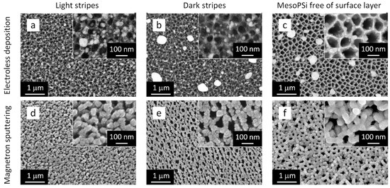
Figure 4.
Top-view SEM images of mesoPSi coated with Ag particles: (a) light stripe of mesoPSi with defective surface layer after electroless deposition of Ag, (b) dark stripe of mesoPSi with defective surface layer after electroless deposition of Ag, (c) mesoPSi free of defective surface layer after electroless deposition of Ag, (d) light stripe of mesoPSi with defective surface layer after magnetron sputtering of Ag, (e) dark stripe of mesoPSi with defective surface layer after magnetron sputtering of Ag, and (f) mesoPSi free of defective surface layer after magnetron sputtering of Ag.
In contrast to the results obtained via electroless deposition, magnetron sputtering produced dense quasi-continuous films composed of Ag NPs, as illustrated in Figure 4d–f. The size and spatial distribution of the resulting Ag NPs look similar on both the light and dark stripes of the mesoPSi surface. However, larger gaps between Ag NPs were observed in the films deposited on the light stripes, as shown in Figure 4d,e and the corresponding insets. Interestingly, the Ag film sputtered onto the defect-free mesoPSi surface presented in Figure 4f exhibits a distinct worm-like morphology, where the elongated Ag NPs conformed to the underlying mesoPSi skeleton, effectively replicating the surface topography of the mesoPSi sample. This resulted in the formation of the structure mimicking so-called silver ‘nanovoids’, which can enable a strong and reproducible SERS response [54].
3.4. Simulation of Electric Field Strength in Silver-Coated Mesoporous Silicon
To further investigate the Ag-coated mesoPSi, we conducted numerical simulations of the electric field strength distribution for the samples with and without the defective surface layer using COMSOL code. The model shown in Figure 5a reflects the morphology observed in the SEM image of Figure 4c, while the model in Figure 5b corresponds to the ‘nanovoid’ structure presented in Figure 4f. In more detail, the cross section of the pore channel is represented as an equilateral hexagon with a side length of 50 nm. Ag NPs are located on the internal pore surface. The geometry of the electroless Ag NPs is imitated by truncated spheres of 10 nm diameter. Ag NPs formed by magnetron sputtering are better described by the semisphere geometry of 25 nm in diameter. Simulation results under 473 nm plane wave excitation indicate stronger electric field strength up to 8.0 × 10⁷ V/m between Ag NPs formed by electroless deposition compared to those formed by magnetron sputtering, which provided the maximal electric field strength equal to 6.4 × 10⁷ V/m in the top parts of the semispheres. This is primarily attributed to the smaller interparticle distances in the electroless-deposited structures. Although the electroless Ag NPs are expected to facilitate a more intensive SERS signal, the Ag semispheres on the pore walls can potentially act as ‘nanovoid’ structure because a mild electric field enhancement is observed in the pore center.
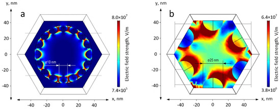
Figure 5.
Simulated electric field strength distribution for mesoPSi free of the defective surface layer coated with Ag NPs by (a) electroless deposition and (b) magnetron sputtering.
3.5. SERS Response from Silver-Coated Mesoporous Silicon
This study evaluates the effectiveness of the developed approach of modifying the mesoPSi surface to improve both spot-to-spot reproducibility and intensity of the SERS signal. To establish these correlations, we compared the morphologies shown in Figure 4 with the corresponding experimental results of the SERS measurements presented in Figure 6a,b. SERS-signatures of 10 M R6G are average spectra calculated from SERS maps collected in dark and light stripes of mesoPSi coated with Ag before the removal of the defected layer and in two spots of Ag-coated mesoPSi free of the defected surface layer.
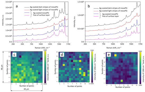
Figure 6.
SERS measurement results for R6G molecules adsorbed from a 10 M solution on Ag particles on mesoPSi. Ag particles were deposited by (a) electroless deposition and (b) magnetron sputtering. In (a,b), the SERS spectra were recorded from dark and light stripe regions on Ag-coated mesoPSi with the defective surface layer as well as from two different areas on Ag-coated mesoPSi free of surface layer. SERS intensity maps of the 1366 cm R6G band (C-C stretching in xantene ring) [55] intensity are shown for Ag coating on (c) mesoPSi free of the defective surface layer as well as on mesoPSi with the defective surface layer in the (d) dark and (e) light stripe regions.
For each Ag-coated mesoPSi sample, a distinct SERS fingerprint was recorded with all characteristic bands of R6G [55]. In accordance with our expectations, the SERS signal intensity varied depending on the underlying mesoPSi surface used as a template for the Ag deposition. Notably, a 2–3 time decrease in SERS intensity was observed when moving from the dark to the light stripes, regardless of the Ag deposition method. In contrast, samples treated with the copper-assisted corrosion method exhibited consistent SERS responses at different measurement points. In addition to the observed intra-sample variability in SERS intensity (i.e., among surface regions coated by the same silver deposition technique), it was also found that Ag particles formed by electroless deposition generally produced a stronger SERS response compared to those formed via magnetron sputtering. These findings align well with the observed difference in the simulation results, as SERS activity depends on the local electromagnetic field enhancement generated by plasmonic nanostructures.
The spot-to-spot reproducibility of the SERS signal was assessed by SERS mapping the Ag-coated mesoPSi samples with and without defected surface layer as shown in Figure 6c,d. The sample free of the defected layer exhibited much more uniform signal intensity across the silver-coated surface. In more detail, removal of the defective surface layer from mesoPSi provided a base for formation of over 65% of the SERS-active area with the signal deviation ±10%. On the other hand, only 12% of the SERS-active area of the Ag-coated mesoPSi surface with the defective layer resulted in the same signal intensity deviation. These results highlight the effectiveness of the developed method in producing stronger and reproducible SERS responses on various silver-covered mesoPSi surfaces.
4. Conclusions
This study presents a novel approach to address the surface structural nonuniformity of mesoPSi, which arises from the uneven distribution of dopant concentration in monocrystalline silicon ingots grown via the Czochralski method. The findings demonstrate that the corrosive copper deposition on pristine mesoPSi samples prior to the formation of the Ag coating, followed by wet etching of the deposited Cu film, effectively reduces spot-to-spot variability in the SERS signal intensity and enhances Raman scattering. Once the defective surface layer was removed, the variation in absolute porosity from sample to sample of mesoPSi was reduced from 5% for freshly prepared mesoPSi to 2% after Cu-assisted corrosion.
This improvement results from exposing the deeper mesoPSi surface, which is largely free from pore irregularities such as bottlenecks and ‘dead’ pores—conditions that are highly favorable for the formation of plasmonic metal nanostructures with well-defined morphology.
The proposed method is not only simple and cost-effective, but is also rapid, requiring only a few minutes to implement.
It was revealed that the spot-to-spot reproducibility of the SERS signal from R6G at micromolar concentration adsorbed on the Ag-coated mesoPSi substrate free of the defected layer exhibited much more uniform intensity level across the surface compared to that before the Cu-assisted treatment. Removal of the defective surface layer from mesoPSi led to formation of over 65% of the SERS-active area with the signal deviation ±10%. In contrast, just 12% of the SERS-active area of the Ag-coated mesoPSi surface with the defective layer resulted in the same signal intensity deviation.
In addition to improving the reproducibility and intensity of SERS signals, the proposed approach enables the fabrication of plasmonic substrates with enhanced control over pore uniformity and metal nanoparticle distribution. This is essential for applications in quantitative analytical chemistry, antibacterial surface engineering for tissue-embedded Si microchips, and optical biosensing, where a uniform electromagnetic field distribution is critical. Moreover, the method holds promise for a broad range of technologies that rely on mesoPSi as a template material.
Author Contributions
Conceptualization, H.V.B. and D.B.; methodology, H.V.B. and D.L.; software, U.S.; validation, D.L., Z.N. and D.J.; formal analysis, H.V.B., A.S., U.S., A.P. and D.B.; investigation, H.V.B., D.L. and A.P.; resources, A.D., A.A. and A.I.P.; data curation, Z.N. and U.S.; writing—original draft preparation, H.V.B. and A.S.; writing—review and editing, A.D., A.A., A.P., E.N., A.I.P. and D.B.; visualization, H.V.B., A.S. and U.S.; supervision, A.D., A.I.P. and D.B.; project administration, A.D. and D.B.; funding acquisition, A.D., A.A., A.I.P. and D.B. All authors have read and agreed to the published version of the manuscript.
Funding
This research has been funded by the Science Committee of the Ministry of Science and Higher Education of the Republic of Kazakhstan (Grant No. AP23487881), the Latvian Scientific Council grant No. LZP-2021/1-0464 and the State Program for Scientific Research of Belarus «Photonics and electronics for innovations» (subtasks Nos. 1.8.2, 2.2.7, and 3.9.5).
Data Availability Statement
The data sets presented in this study are available within the article.
Conflicts of Interest
The authors declare no conflicts of interest.
References
- Herino, R.; Bomchil, G.; Barla, K.; Bertrand, C.; Ginoux, J.L. Porosity and Pore Size Distributions of Porous Silicon Layers. J. Electrochem. Soc. 1987, 134, 1994–2000. [Google Scholar] [CrossRef]
- Uhlir, A. Electrolytic Shaping of Germanium and Silicon. Bell Syst. Tech. J. 1956, 35, 333–347. [Google Scholar] [CrossRef]
- Bomchil, G.; Halimaoui, A.; Herino, R. Porous silicon: The material and its applications to SOI technologies. Microelectron. Eng. 1988, 8, 293–310. [Google Scholar] [CrossRef]
- Imai, K. A new dielectric isolation method using porous silicon. Solid State Electron. 1981, 24, 159–164. [Google Scholar] [CrossRef]
- Lang, W.; Steiner, P.; Richter, A.; Marusczyk, K.; Weimann, G.; Sandmaier, H. Application of porous silicon as a sacrificial layer. Sens. Actuators A Phys. 1994, 43, 239–242. [Google Scholar] [CrossRef]
- Ge, M.; Fang, X.; Rong, J.; Zhou, C. Review of porous silicon preparation and its application for lithium-ion battery anodes. Nanotechnology 2013, 24, 422001. [Google Scholar] [CrossRef]
- Maiello, G.; La Monica, S.; Ferrari, A.; Masini, G.; Bondarenko, V.; Dorofeev, A.; Kazuchits, N. Light guiding in oxidised porous silicon optical waveguides. Thin Solid Film. 1997, 297, 311–313. [Google Scholar] [CrossRef]
- Torres-Costa, V.; Martín-Palma, R.J. Application of nanostructured porous silicon in the field of optics. A review. J. Mater. Sci. 2010, 45, 2823–2838. [Google Scholar] [CrossRef]
- Theiß, W. Optical properties of porous silicon. Surf. Sci. Rep. 1997, 29, 91–192. [Google Scholar] [CrossRef]
- Shatskaia, M.; Nazarovskaia, D.; Gonchar, K.; Lomovskaya, Y.; Tsiniaikin, I.; Shalygina, O.; Kudryavtsev, A.; Osminkina, L. Photoluminescent porous silicon nanowires as contrast agents for bioimaging. Condens. Matter Interphases 2024, 26, 161–167. [Google Scholar] [CrossRef]
- Fan, D.; De Rosa, E.; Murphy, M.B.; Peng, Y.; Smid, C.A.; Chiappini, C.; Liu, X.; Simmons, P.; Weiner, B.K.; Ferrari, M.; et al. Mesoporous Silicon-PLGA Composite Microspheres for the Double Controlled Release of Biomolecules for Orthopedic Tissue Engineering. Adv. Funct. Mater. 2012, 22, 282–293. [Google Scholar] [CrossRef]
- Li, W.; Liu, Z.; Fontana, F.; Ding, Y.; Liu, D.; Hirvonen, J.T.; Santos, H.A. Tailoring Porous Silicon for Biomedical Applications: From Drug Delivery to Cancer Immunotherapy. Adv. Mater. 2018, 30, 1703740. [Google Scholar] [CrossRef] [PubMed]
- Salonen, J.; Mäkilä, E. Thermally Carbonized Porous Silicon and Its Recent Applications. Adv. Mater. 2018, 30, 1703819. [Google Scholar] [CrossRef]
- Kumar, P.; Huber, P. Effect of Etching Parameter on Pore Size and Porosity of Electrochemically Formed Nanoporous Silicon. J. Nanomater. 2007, 2007, 1–4. [Google Scholar] [CrossRef]
- Kuntyi, O.; Zozulya, G.; Shepida, M. Porous Silicon Formation by Electrochemical Etching. Adv. Mater. Sci. Eng. 2022, 2022, 1–15. [Google Scholar] [CrossRef]
- Kochylas, I.; Gardelis, S.; Likodimos, V.; Giannakopoulos, K.; Falaras, P.; Nassiopoulou, A. Improved Surface-Enhanced-Raman Scattering Sensitivity Using Si Nanowires/Silver Nanostructures by a Single Step Metal-Assisted Chemical Etching. Nanomaterials 2021, 11, 1760. [Google Scholar] [CrossRef]
- Linevych, Y.; Koval, V.; Dusheiko, M.; Lakyda, M. Application of silicon nanowires in sensors of temperature, light and humidity. Mater. Sci. Semicond. Process. 2024, 184, 108773. [Google Scholar] [CrossRef]
- Boukhvalov, D.; Zhumabay, B.; Kusherovab, P.; Rakymetovb, B.; Tynyshtykbayev, K.; Serikkanov, S.; Chuchvag, N. One step large-scale preparation of silicon-based efficient solar vapor generators. RSC Adv. 2025, 15, 6794–6802. [Google Scholar] [CrossRef]
- Cullis, A.G.; Canham, L.T.; Calcott, P.D.J. The structural and luminescence properties of porous silicon. J. Appl. Phys. 1997, 82, 909–965. [Google Scholar] [CrossRef]
- Cullis, A.G.; Canham, L.T. Visible light emission due to quantum size effects in highly porous crystalline silicon. Nature 1991, 353, 335–338. [Google Scholar] [CrossRef]
- Low, S.P.; Voelcker, N.H. Biocompatibility of Porous Silicon. In Handbook of Porous Silicon; Canham, L., Ed.; Springer International Publishing: Berlin/Heidelberg, Germany, 2014; pp. 533–545. [Google Scholar] [CrossRef]
- Shabir, Q. Biodegradability of Porous Silicon. In Handbook of Porous Silicon; Canham, L., Ed.; Springer International Publishing: Berlin/Heidelberg, Germany, 2014; pp. 1–7. [Google Scholar] [CrossRef]
- Tzur-Balter, A.; Shtenberg, G.; Segal, E. Porous silicon for cancer therapy: From fundamental research to the clinic. Rev. Chem. Eng. 2015, 31, 193–207. [Google Scholar] [CrossRef]
- Beale, M.I.J.; Chew, N.G.; Uren, M.J.; Cullis, A.G.; Benjamin, J.D. Microstructure and formation mechanism of porous silicon. Appl. Phys. Lett. 1985, 46, 86–88. [Google Scholar] [CrossRef]
- Dasgupta, N.P.; Liu, C.; Andrews, S.; Prinz, F.B.; Yang, P. Atomic Layer Deposition of Platinum Catalysts on Nanowire Surfaces for Photoelectrochemical Water Reduction. J. Am. Chem. Soc. 2013, 135, 12932–12935. [Google Scholar] [CrossRef] [PubMed]
- Dolgyi, A.; Bandarenka, H.; Prischepa, S.; Yanushkevich, K.; Nenzi, P.; Balucani, M.; Bondarenko, V. Electrochemical Deposition of Ni into Mesoporous Silicon. ECS Trans. 2012, 41, 111–118. [Google Scholar] [CrossRef]
- Granitzer, P.; Rumpf, K. Porous Silicon—A Versatile Host Material. Materials 2010, 3, 943–998. [Google Scholar] [CrossRef]
- Koda, R.; Fukami, K.; Sakka, T.; Ogata, Y.H. Electrodeposition of platinum and silver into chemically modified microporous silicon electrodes. Nanoscale Res. Lett. 2012, 7, 330. [Google Scholar] [CrossRef]
- Kim, T.; Braun, G.; She, Z.; Hussain, S.; Ruoslahti, E.; Sailor, M. Composite porous silicon–silver nanoparticles as theranostic antibacterial agents. ACS Appl. Mater. Interfaces 2016, 8, 30449–30457. [Google Scholar] [CrossRef]
- Alhmoud, H.; Cifuentes-Rius, A.; Delalat, B.; Lancaster, D.; Voelcker, N. Gold-Decorated Porous Silicon Nanopillars for Targeted Hyperthermal Treatment of Bacterial Infections. ACS Appl. Mater. Interfaces 2017, 9, 33707–33716. [Google Scholar] [CrossRef]
- Virga, A.; Rivolo, P.; Frascella, F.; Angelini, A.; Descrovi, E.; Geobaldo, F.; Giorgis, F. Silver Nanoparticles on Porous Silicon: Approaching Single Molecule Detection in Resonant SERS Regime. J. Phys. Chem. C 2013, 117, 20139–20145. [Google Scholar] [CrossRef]
- Alwan, A.M.; Naseef, I.A.; Dheyab, A.B. Well Controlling of Plasmonic Features of Gold Nanoparticles on Macro Porous Silicon Substrate by HF Acid Concentration. Plasmonics 2018, 13, 2037–2045. [Google Scholar] [CrossRef]
- Ge, D.; Wei, J.; Ding, J.; Zhang, J.; Ma, C.; Wang, M.; Zhang, L.; Zhu, S. Silver Nano-Dendrite-Plated Porous Silicon Substrates Formed by Single-Step Electrochemical Synthesis for Surface-Enhanced Raman Scattering. ACS Appl. Nano Mater. 2020, 3, 3011–3018. [Google Scholar] [CrossRef]
- Redko, S.; Dolgiy, A.; Zhygulin, D.; Khaliava, V.; Khinevich, N.; Zavatski, S.; Bandarenka, H. Fabrication and simulation of silver nanostructures on different types of porous silicon for surface enhanced Raman spectroscopy. In Proceedings of the Physics and Simulation of Optoelectronic Devices XXVII, San Francisco, CA, USA, 2–7 February 2019; p. 61. [Google Scholar] [CrossRef]
- Gold, V.; Loening, K.L.; McNaught, A.D.; Shemi, P. The IUPAC Compendium of Chemical Terminology: The Gold Book; Blackwell Scientific Publications: Oxford, UK, 2019. [Google Scholar] [CrossRef]
- Martín-Sánchez, D.; Ponce-Alcántara, S.; Martínez-Pérez, P.; García-Rupérez, J. Macropore Formation and Pore Morphology Characterization of Heavily Doped p-Type Porous Silicon. J. Electrochem. Soc. 2019, 166, B9–B12. [Google Scholar] [CrossRef]
- Ouyang, H.; Christophersen, M.; Fauchet, P.M. Enhanced control of porous silicon morphology from macropore to mesopore formation. Phys. Status Solidi (a) 2005, 202, 1396–1401. [Google Scholar] [CrossRef]
- Bandarenka, H.V.; Girel, K.V.; Zavatski, S.A.; Panarin, A.; Terekhov, S.N. Progress in the Development of SERS-Active Substrates Based on Metal-Coated Porous Silicon. Materials 2018, 11, 852. [Google Scholar] [CrossRef]
- Jabbar, A.A.; Alwan, A.M.; Haider, A.J. Modifying and Fine Controlling of Silver Nanoparticle Nucleation Sites and SERS Performance by Double Silicon Etching Process. Plasmonics 2018, 13, 1171–1182. [Google Scholar] [CrossRef]
- Kosović, M.; Balarin, M.; Ivanda, M.; Đerek, V.; Marciuš, M.; Ristić, M.; Gamulin, O. Porous Silicon Covered with Silver Nanoparticles as Surface-Enhanced Raman Scattering (SERS) Substrate for Ultra-Low Concentration Detection. Appl. Spectrosc. 2015, 69, 1417–1424. [Google Scholar] [CrossRef]
- Zavatski, S.; Khinevich, N.; Girel, K.; Redko, S.; Kovalchuk, N.; Komissarov, I.; Lukashevich, V.; Semak, I.; Mamatkulov, K.; Vorobyeva, M.; et al. Surface Enhanced Raman Spectroscopy of Lactoferrin Adsorbed on Silvered Porous Silicon Covered with Graphene. Biosensors 2019, 9, 34. [Google Scholar] [CrossRef]
- Natan, M.J. Concluding Remarks: Surface enhanced Raman scattering. Faraday Discuss. 2006, 132, 321. [Google Scholar] [CrossRef]
- Errien, N.; Vellutini, L.; Louarn, G.; Froyer, G. Surface characterization of porous silicon after pore opening processes inducing chemical modifications. Appl. Surf. Sci. 2007, 253, 7265–7271. [Google Scholar] [CrossRef]
- Khinevich, N.; Juodėnas, M.; Tamulevičienė, A.; Bandarenka, H.; Tamulevičius, S. Tailoring Mesoporous Silicon Surface to Form a Versatile Template for Nanoparticle Deposition. Coatings 2021, 11, 699. [Google Scholar] [CrossRef]
- Bandarenka, H.; Artsemyeva, K.; Redko, S.; Panarin, A.; Terekhov, S.; Bondarenko, V. Effect of swirl-like resistivity striations in n+ -type Sb doped Si wafers on the properties of Ag/porous silicon SERS substrates. Phys. Status Solidi C 2013, 10, 624–627. [Google Scholar] [CrossRef]
- Henins, I. Precision density measurement of silicon. J. Res. Natl. Bur. Stand. U.S. Sect. A Phys. Chem. 1964, 68A, 529. [Google Scholar] [CrossRef]
- COMSOL AB, version 5.3. COMSOL Multiphysics®. COMSOL: Stockholm, Sweden, 2017.
- Bandarenka, H.; Adinehloo, D.; Oskolkov, E.; Kuzmin, A.; Pliss, A.; Shaibu, O.; Bird, J.; Baev, A.; Perebeinos, V.; Prasad, P. Third-Harmonic Generation Imaging of Local Doping, Mechanical Stress, and Stray Electric Fields in Silicon Microchips. ACS Photonics 2025, 12, 2304–2310. [Google Scholar] [CrossRef]
- Corsetti, F.; Mostofi, A. A first-principles study of As doping at a disordered Si-SiO2 interface. J. Phys. Condens. Matter. 2013, 26, 055002. [Google Scholar] [CrossRef]
- Goryachev, D.N.; Belyakov, L.V.; Sreseli, O.M. On the mechanism of porous silicon formation. Semiconductors 2000, 34, 1090–1093. [Google Scholar] [CrossRef]
- Smith, R.L.; Collins, S.D. Porous silicon formation mechanisms. J. Appl. Phys. 1992, 71, R1–R22. [Google Scholar] [CrossRef]
- Morinaga, H.; Suyama, M.; Ohmi, T. Mechanism of Metallic Particle Growth and Metal-Induced Pitting on Si Wafer Surface in Wet Chemical Processing. J. Electrochem. Soc. 1994, 141, 2834–2841. [Google Scholar] [CrossRef]
- Bandarenka, H.; Redko, S.; Nenzi, P.; Balucani, M.; Bondarenko, V. Optimization of chemical displacement deposition of copper on porous silicon. J. Nanosci. Nanotechnol. 2012, 12, 8725–8731. [Google Scholar] [CrossRef]
- Artsemyeva, K.; Dolgiy, A.; Bandarenka, H.; Panarin, A.; Khodasevich, I.; Terekhov, S.; Bondarenko, V. Fabrication of SERS-Active Substrates by Electrochemical and Electroless Deposition of Metals in Macroporous Silicon. ECS Trans. 2013, 53, 85–95. [Google Scholar] [CrossRef]
- Majoube, M.; Henry, M. Fourier Transform Raman and Infrared and Surface-Enhanced Raman Spectra for Rhodamine 6G. Spectrochim. Acta A Mol. Spectrosc. 1991, 47, 1459–1466. [Google Scholar] [CrossRef]
Disclaimer/Publisher’s Note: The statements, opinions and data contained in all publications are solely those of the individual author(s) and contributor(s) and not of MDPI and/or the editor(s). MDPI and/or the editor(s) disclaim responsibility for any injury to people or property resulting from any ideas, methods, instructions or products referred to in the content. |
© 2025 by the authors. Licensee MDPI, Basel, Switzerland. This article is an open access article distributed under the terms and conditions of the Creative Commons Attribution (CC BY) license (https://creativecommons.org/licenses/by/4.0/).