1. Introduction
To date, the International Space Station (ISS) is the space platform with the highest power generation capability, producing and distributing 105 kW [
1]. The next space station, currently under development, is the Lunar Gateway, which is expected to handle 32 kW [
2]. In both cases, power is generated by solar panels and a 120 V regulated bus voltage distribution is achieved through direct energy transfer (DET) power processors.
The current European space standard ECSS-E-ST-20C Rev.2 [
3] defines the standard for regulated bus voltage at different power ranges up to 120 V. The standard states that 100 V or 120 V bus voltage is adequate in the range of 8 kW and 20 kW. However, for higher power levels, compliance with the standard becomes difficult in both static (large DC bus current) and dynamic (very low output impedance).
Table 1 summarizes the different voltage and power ranges required to meet the strict output impedance mask dictated by [
3].
Larger space power systems are expected to arrive in the coming decades. Lunar bases and space stations would demand approximately 100–300 kW [
4], and the initial attempts at space-based solar power will be in the MW range [
5,
6]. In all cases, these systems would be built in phases, resulting in the growth of the power requirement with each step taken, potentially surpassing initial design projections. Consequently, there is a substantial need for adaptable and scalable power generation and distribution systems capable of accommodating diverse requirements throughout each phase of deployment.
Different options have been considered for power systems in the order of hundreds of kW to few MW. One possibility is to use photovoltaic (PV) solar panels as the main power generator. The ISS has reached a total solar power production of 100 kW with an efficiency of 14.5% [
1], and the new generation of European solar arrays for telecommunication satellites achieved a power production of 28.7 kW with an efficiency of 28.5% [
7]. The main advantage of using solar arrays is the scalability and integration with the rest of the platform; however, for solar arrays operating above 150–200 V there are technical challenges to be solved [
8].
Nuclear fission-based energy systems using Stirling engines have also been proposed for power ranges of tens of kW. However, this technology is not as mature as PV and scalability up to the hundred-kW range is not considered at this moment [
9,
10].
Regarding the electrical architecture, different solutions are explored to distribute high voltage (HV). In [
11], a 1-kV bus is proposed for space solar power purposes. In [
12,
13], different power system architectures are studied for a lunar base. Both DC and AC microgrids might coexist, with typical voltages ranging from 120 V to 600 V. A common point in these examples is the significant distance between the PV generators and the end users. Therefore, the use of converters to integrate the PV generators into the distribution bus would be critical to provide regulation, galvanic isolation, and high voltage distribution. In this regard, the architecture described in [
11] employs phase-shifted zero-voltage switching (ZVS) full-bridge converters in an Input Parallel Output Series (IPOS) configuration. A similar idea is proposed by the authors in [
14], but the architecture is based on the current-fed zero-voltage zero-current switching (ZVZCS) direct current transformer (DCX) converter, described in [
15]. Bus regulation is achieved using the Sequential Switching Shunt Regulator (S3R) technique, which consists of a sequential control of the DCX modules using a hysteretic controller [
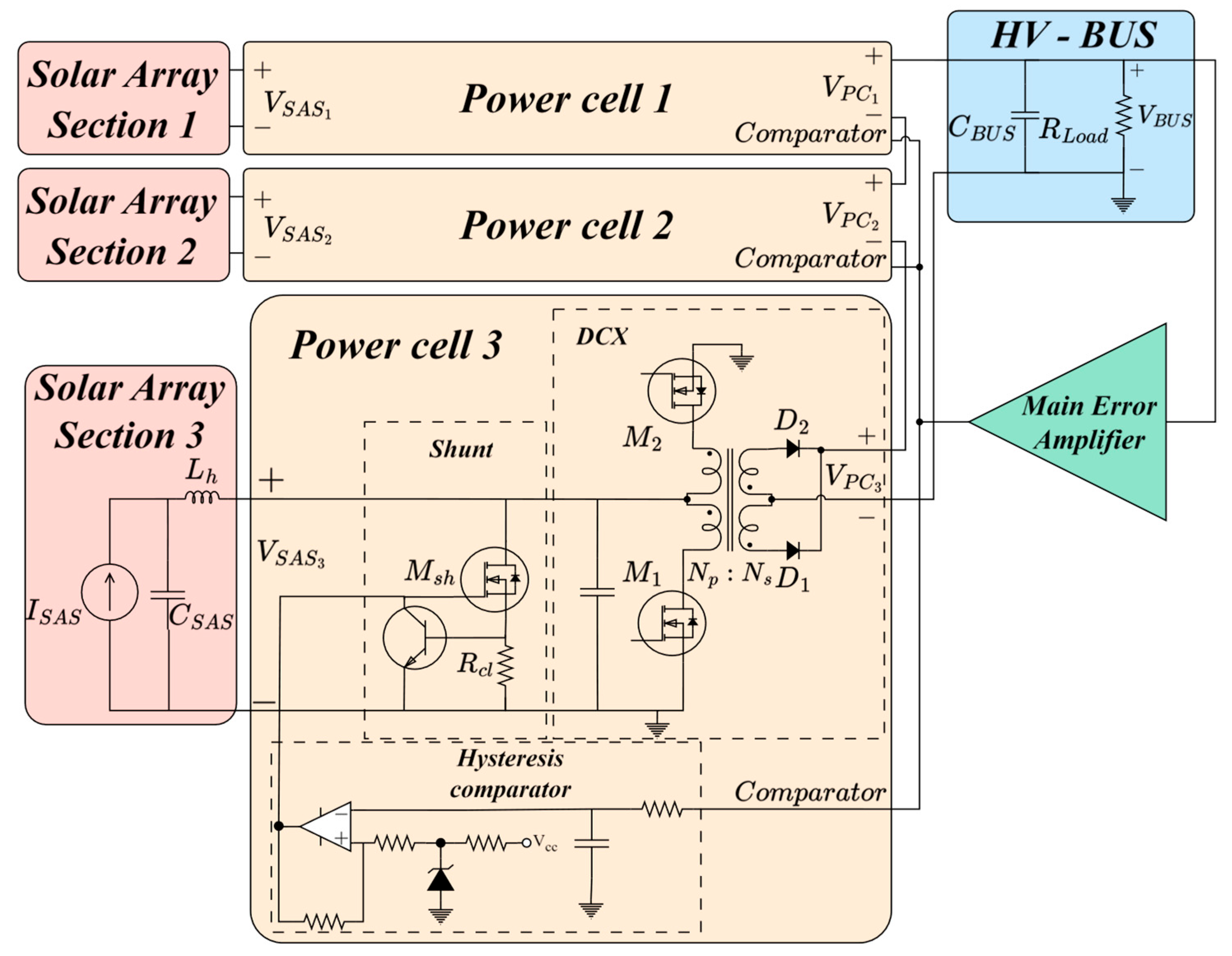
16]. Each power cell can be connected as an Input Independent Output Series (IIOS) configuration instead of IPOS for improved reliability. The main advantages of this approach are its simple switching control, regulation, and modularity. Moreover, the current-fed converter operates well with a solar array at the input. Furthermore, to keep the simplest transistor-driving approach, a push-pull and center-tapped full-wave rectifier structure is considered; see
Figure 1. An explanation of the terms can be found in Table 4. On top of that, derating rules [
17], limited availability of space-qualified parts [
18], and high voltage isolation requirements [
19] make the IIOS converter the most suitable approach. The architecture proposal is named by the authors as S3DCX.
The main research points of this article include a review of the state of the technology and availability of HV SiC Schottky diodes for space applications, with a focus on their voltage rating under the impact of high-energy particles. Additionally, this article covers the design and experimental validation of serialized DCX converters to achieve 600 V and 900 V distribution bus based on the S3DCX presented in [
14]. The research also investigates the electric isolation of the DCX transformer and power cell in vacuum and partial pressure conditions.
Finally, this article is organized as follows.
Section 2 analyses the requirements and derating needed to apply semiconductors for HV space applications.
Section 3 details the serialization of the S3DCX to achieve 600 V and 900 V distribution bus.
Section 4 presents the experimental validation of the output serialized S3DCX, the effects of the converter in vacuum, and partial pressure conditions.
Section 5 discusses the experimental results.
Section 6 concludes the article.
2. Power Semiconductor Industry Market Research, Trends, and Selection
The harsh environment of space requires a selection of components that can work properly during the length of the mission. The European Space Standard ECSS-Q-ST-30-11C Rev.2 [
17] is applied to avoid excess stress that could damage the components. In the S3DCX, MOSFETs and diodes are the most affected by the derating in the circuit. In general, power Field-Effect Transistors (FETs) must be 80% limited in V
DS and 75% in I
DS with respect to the maximum rating, and rectifier diodes must be 75% limited in I
F and V
R as well.
In a space environment, high-energy particles could impact the semiconductors, degrading their electrical properties or inducing a Single Event Breakdown (SEB). Depending on the transferred energy, defined by the Linear Energy Transfer (LET), the SEB will occur at different voltages. Therefore, it is crucial to ensure that the operating voltages remain within the safe operating area of the selected component.
Taking the proposal of this paper as a study case, 100 V is considered on the primary side of the power cell. So, the shunt FET (M
sh) and DCX FETs (M
1, M
2) must be rated, after derating, for a minimum of 125 V and 250 V, respectively. There are commercially available 250-V space-qualified MOSFETs that can sustain high LET at the rated voltage. In
Table 2, a 250 V-45 A space-qualified MOSFET and a commercial equivalent have been selected for implementation in the prototype.
Wide-Bandgap (WBG) FETs are considered for use in space applications due to their lower power losses, ability to operate at higher switching frequencies, and smaller size compared to conventional Si FETs [
20,
21]. A demonstrator for an electrical propulsion power processing unit using Silicon Carbide (SiC) MOSFETs, operating at a maximum 500 V output voltage and 15 kW, has been tested, and the authors claim better performances compared to Si MOSFETs [
22]. One challenge that makes it difficult to use WBG semiconductors is the significant derating required relative to their rated value to avoid SEB [
23,
24].
On the diodes side, for a 300-V output voltage, Schottky diodes are needed with a maximum repetitive peak reverse voltage (V
RRM) rating of 800 V after applying the derating and a minimum SEB threshold of 600 V. Nowadays, the maximum rating in Si Schottky diodes is 150 V [
25], making them unsuitable for this application. An alternative is to use SiC Schottky diodes, rated up to 1.7 kV, with a lower recovery charge compared to the Si counterpart. One important aspect, as with FETs, is the large derating needed to avoid SEB. Different methods are being studied to improve it. In [
26], simulations show that 1.2-kV SiC Schottky diodes are immune to SEB up to 800 V by using a lateral distribution of the semiconductor layers. In [
27], charge-balanced regions between layers are introduced to improve the electric field distribution during a single event for 3.0-kV SiC Schottky diodes.
Figure 2 shows compiled different radiation test results for Si radiation-hardened (rad-hard) Schottky diodes [
25]; commercial SiC Schottky diodes rated for 650 V [
28], 1.2 kV [
27,
28,
29,
30,
31,
32,
33], and 1.7 kV [
28]; and laboratory SiC Schottky diodes rated for 3.0 kV [
27]. SiC diodes rated for 1.2 kV and 1.7 kV must be derated to 200 V to avoid a SEB. It is shown that experimental 3.0-kV SiC diodes have a SEB threshold of 800 V, making them potential candidates for this kind of application.
From the analysis, it can be concluded that HV rad-hard SiC Schottky diodes are currently unavailable for space applications. Further technological development of SiC Schottky diodes is required to improve their reliability. Commercial SiC Schottky diodes could be used after applying a significant voltage derating [
20], but additional studies regarding their suitability in a space environment are needed.
For the prototype development, and due to the lack of commercial SiC diodes of higher voltage, 1.2-kV SiC diodes have been selected, with the possibility of being replaced by 3.0-kV SiC diodes [
27]. For the component selection, the Figure of Merit (FoM) (1) is utilized, which compares the forward voltage and the capacitive charge of the diodes. A lower FoM value indicates a better overall performance. The DCX operates under soft-switching conditions, so the capacitive charge of the diode will not significantly impact the losses but will affect the switching frequency.
Table 3 summarizes a selection of commercially available SiC Schottky diodes rated for 1.2 kV-10 A and, for comparison purposes, a space-qualified 150 V-20 A Si Schottky diode. Due to the lack of commercial devices and to ensure proper functioning in the worst-case scenario, the STPSC10H12 diode has been selected.
3. Power Cell Serialization for High-Voltage Range
To regulate and increase the voltage from the solar panels to an HV distribution bus, the S3DCX topology [
14] has been chosen. This topology allows each power cell to increase the input voltage of the solar arrays to an intermediate level and then serialize the outputs of each power cell to achieve the desired HV.
As shown in
Figure 1, each power cell consists of three parts: a DCX converter implemented as a resonant ZVZCS push-pull converter, a MOSFET with a current limiter that shunts the Solar Array Section (SAS) to regulate the power cell voltage through controlled switching at a variable duty cycle, and a hysteresis comparator to control the regulation. Different power cells can be connected in parallel and controlled in a sequential manner for each hysteresis comparator by a main error amplifier (MEA).
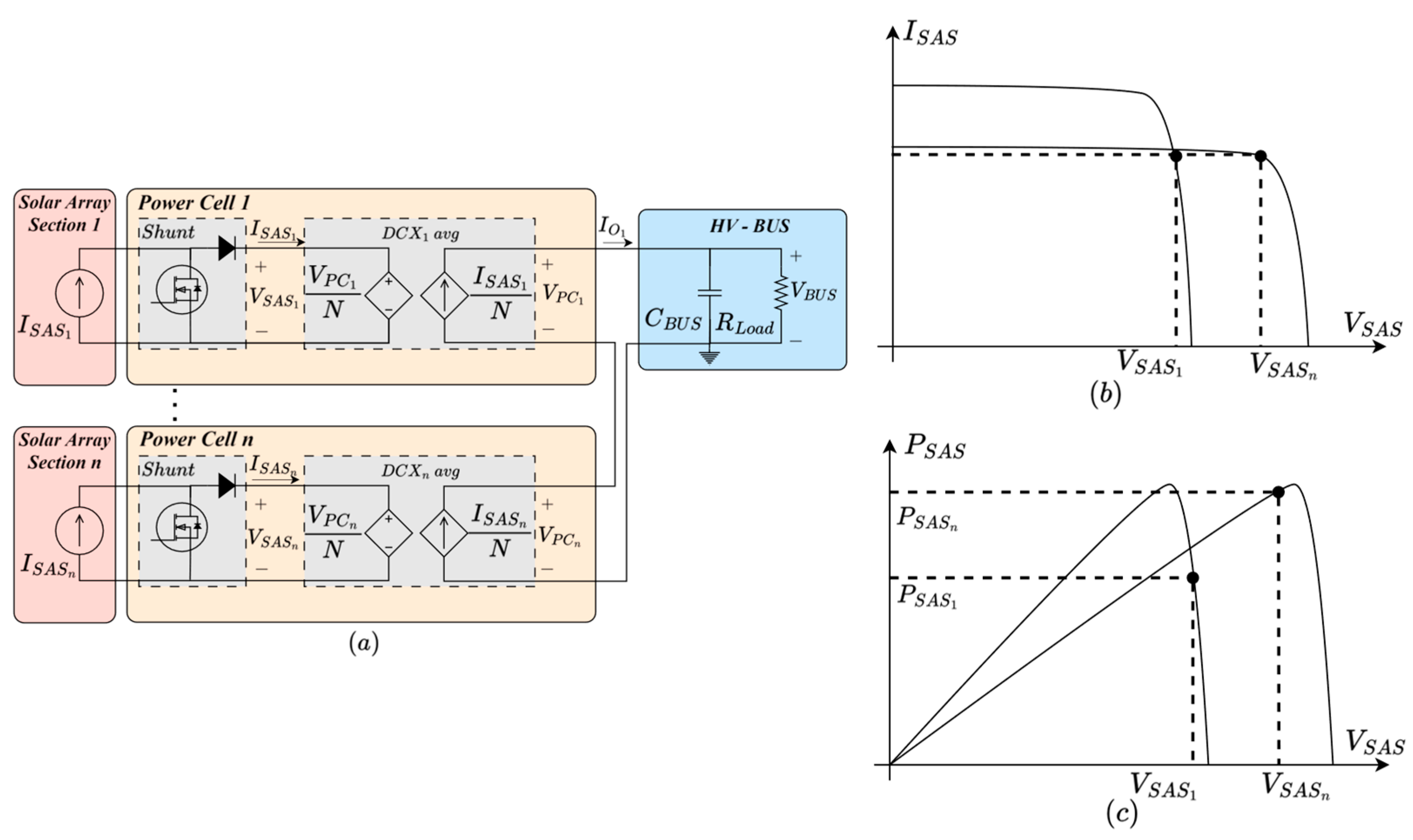
The DCX can be analysed as an average model with a dependent voltage source at the input and a dependent current source at the output, as shown in
Figure 3a. When the outputs of the DCXs are serialized, the bus voltage is the sum of the output voltage of each power cell, as defined in (2).
Following the averaged model, when current sources are connected in series at the output of each power cell, each SAS must deliver the same current, following the condition in (3), where I
SAS mean the current from the SAS, I
O the output current from the serialized power cells, and N the transformation ratio. If the I/V curves of the solar arrays are not identical, as shown in
Figure 3b, the SAS with the lowest current will force the other SAS to operate on the right side of the curve, adjusting the voltage of each panel to reach an equilibrium point that satisfies (2), as demonstrated experimentally in [
14]. A significant mismatch between SASs will have an impact on the overall power generation, as the operating point will be far from the maximum power point of the SAS, as shown in
Figure 3c.
A high-power space platform requires a large number of SASs due to the maximum power each SAS can generate, which is around 2 kW [
7]. The power cells are connected in series to form a string, and these strings are connected in parallel to achieve the specified power output. Given the large number of SASs required, variations in temperature and irradiance can occur between different strings, reducing the power generated in the affected strings. Unbalanced solar arrays within the same string are less likely to occur since they are physically close and, therefore, affected by similar operating conditions. At the system level, the impact of unbalanced strings can be minimised by adopting an architecture with multiple distribution buses, where each bus groups strings that operate under similar conditions. This approach could be beneficial in scalable high-power space platforms that expand over time, as it facilitates the deployment of solar groups and increases reliability compared to using a single distribution bus.
Computer simulation models in SPICE have been performed to validate the serialization of S3DCX. Each SAS is 100 V-4 A, and each power cell converts the output at 300 V. With two cells serialized, a 25% power step load simulation has been performed in
Figure 4. The control loop has been designed to fulfil the requirements of the maximum voltage ripple defined in [
3].
In
Figure 5, a second simulation with unbalanced SASs from 4 A to 2 A and three power cells connected in series to a constant power load has been performed. A constant current of 2 A is supplied by each SAS but at different voltages. Due to the regulation of the voltage, the sum of the three outputs of the power cells remains at 900 V. The control loop has been designed to fulfil the requirements of [
3].
4. Experimental Results
An S3DCX prototype has been implemented. Several tests have been carried out to validate the serialized power cells to achieve an HV distribution bus and study the behaviour and insulation of the converter in vacuum and partial pressure conditions.
4.1. Validation of a Serialized DCXs
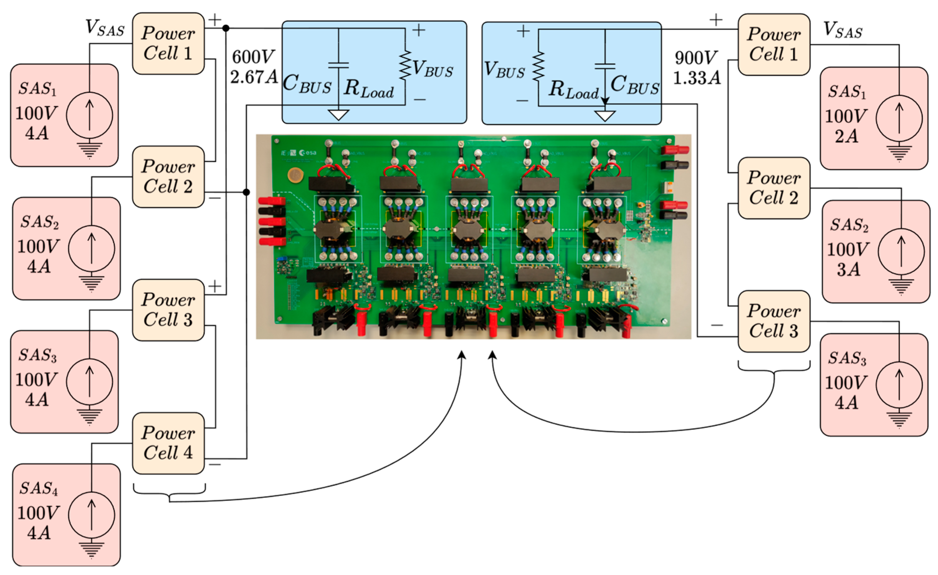
Each power cell has been implemented for a power rating of 400 W, converting 100 V from the solar array to 300 V at the output of each power cell. By connecting the outputs in series, 600 V and 900 V distribution buses are achieved, as shown in
Figure 6. Each power cell and SAS is designed and configured with the parameters defined in
Table 4. The same prototype board is used for both 600 V and 900 V distribution bus, but only one can be active at a time. Swapping between configurations involves reconnecting the output series of the power cells and using the same signal from the hysteresis comparator for each string.
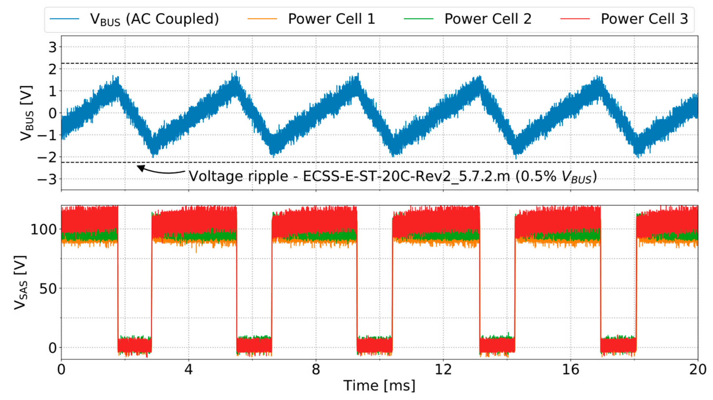
In a 2s2p configuration, as in
Figure 6 (left), a power step load from 600 W to 1 kW has been performed for a 600 V bus. In
Figure 7, during low power load, power cells 1 and 2 operate simultaneously to regulate the output voltage, while power cells 3 and 4 are off. After the step load, power cells 1 and 2 are on, but the power delivered is insufficient to the higher power demand and, therefore, power cells 3 and 4 deliver power at a given duty cycle to regulate the bus voltage. The voltage is stabilized after 6 ms. The steady voltage ripple is 1.6 V, which does not exceed the requirement of 0.5% of the bus voltage (3 V), as defined in the European Space standard in clause 5.7.2.m [
3].
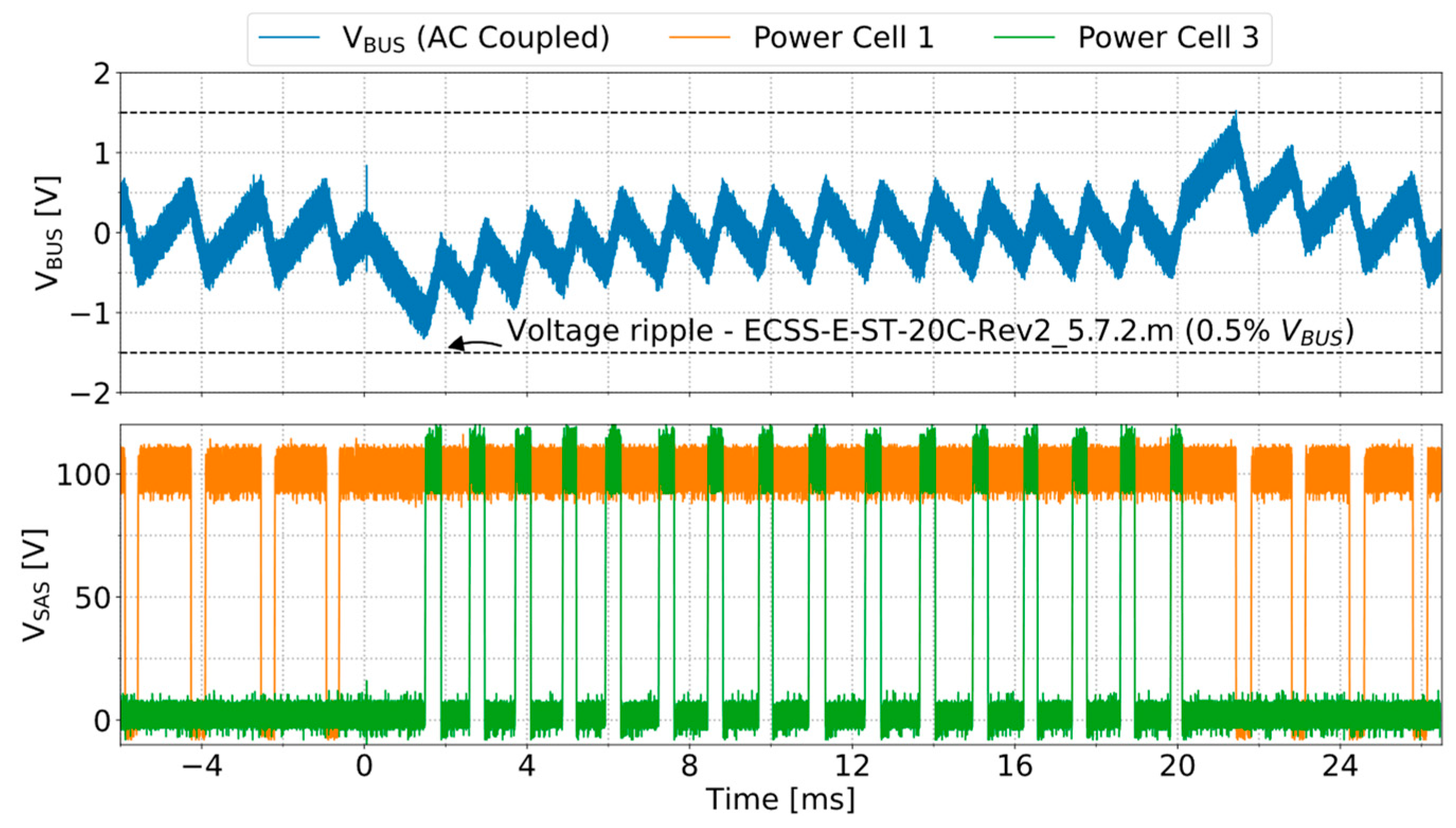
In a 3s1p configuration, as shown in
Figure 6 (right), a steady power load of 800 W has been applied for a 900 V bus. Each solar array simulator is configured to operate within a current range of 2 A to 4 A, generating unbalanced inputs between the serialized power cells and forcing the current of the lower SAS. As a result, a difference in the solar array voltages can be observed at the input of the power cells, as shown in
Figure 8. Despite the unbalanced SAS, the voltages of each SAS reach an equilibrium, ensuring that their combined output equals 900 V of the regulated bus. The steady voltage ripple is measured at 3.5 V, which does not exceed the requirement of 0.5% of the bus voltage (4.5 V).
4.2. Power Cell in Vacuum Conditions
In the European space standard, more than 200 V is considered HV and becomes an important design factor to avoid partial discharges, corona discharges, or arcing that could affect or damage the spacecraft [
19]. To validate the S3DCX under space environment conditions, an isolation test of the DCX transformer and power cell was conducted in vacuum and partial pressure conditions, according to [
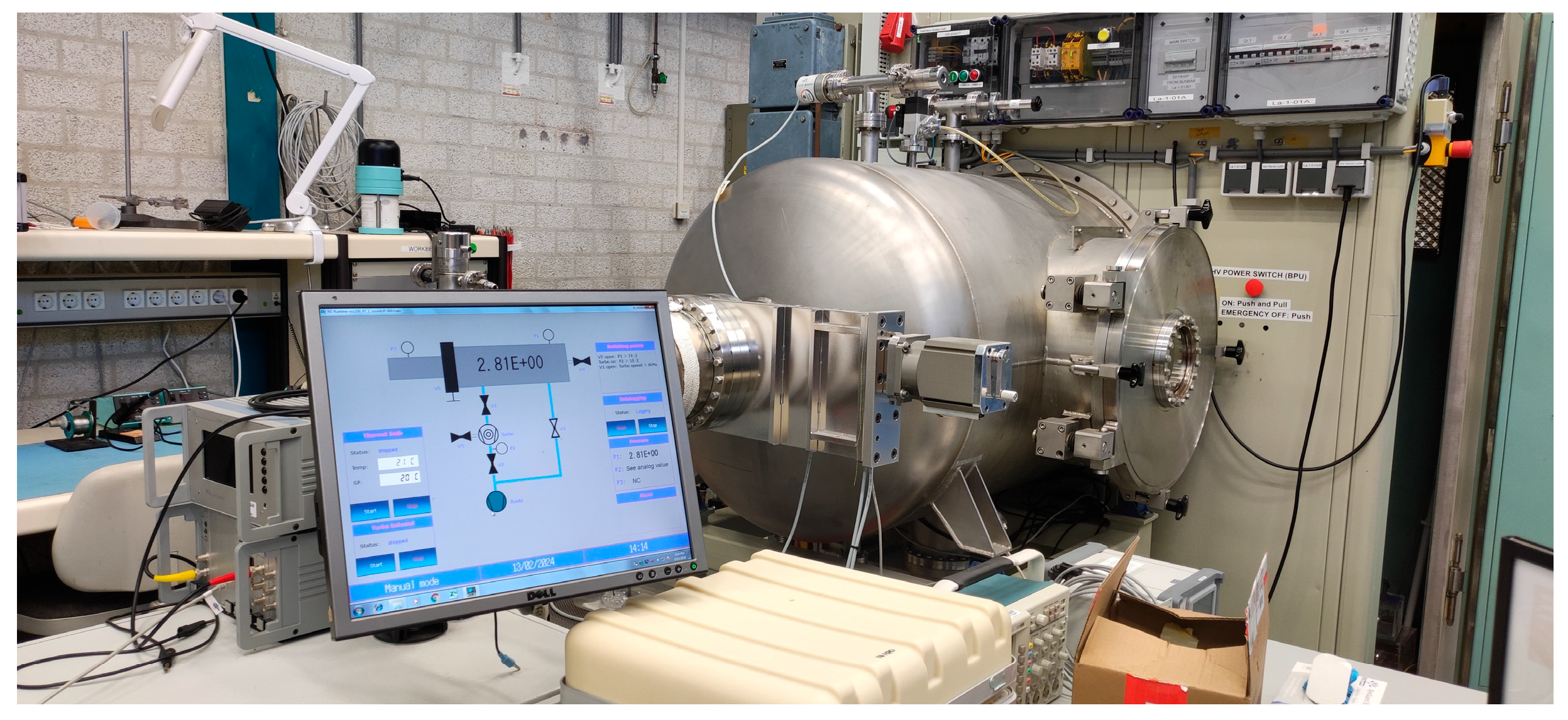
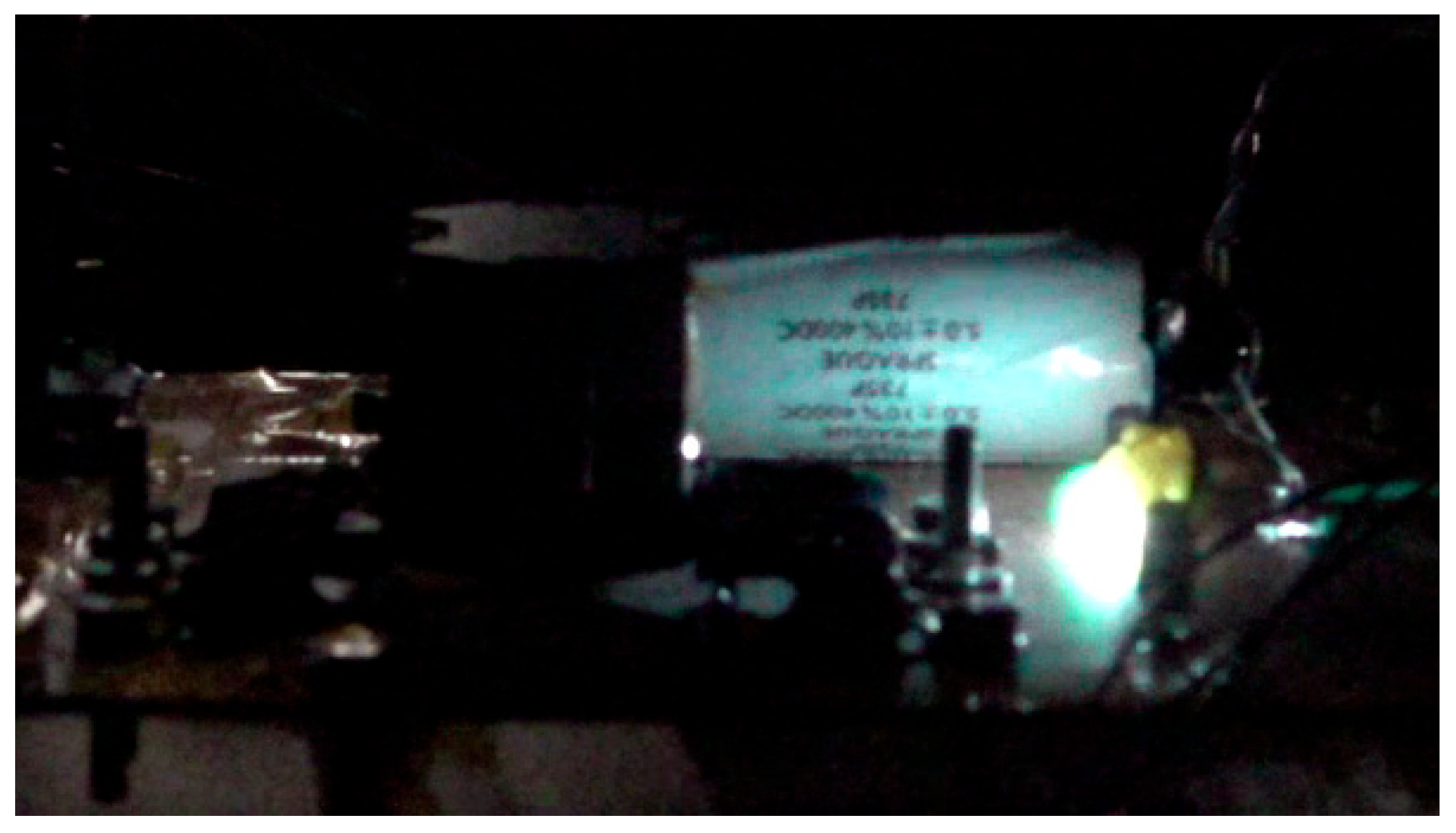
19]. The tests were performed in the high-voltage laboratories of the European Space Research and Technology Centre (ESTEC) of the ESA. The experimental setup is shown in
Figure 9.
The DCX is implemented in a push-pull topology with a 300 V output, resulting in up to 600 V between the transformer windings. In ambient pressure, a non-destructive test was performed to check the dielectric withstanding voltage between the windings using a JP30A as equipment. For a duration of one minute for each pair of windings and in every combination, 600 V and 1.2 kV were supplied. In both cases, a leakage current under 1 µA was observed (isolation resistance > 10 GΩ), confirming that the DCX transformer can isolate voltages up to 1.2 kV.
During the Launch and Early Operation Phase (LEOP), the spacecraft is not completely depressurized, and partial pressures exist, creating the necessary conditions for corona discharge. The DCX transformer, being susceptible to such conditions, was tested in a vacuum chamber over a range of pressures from 10
3 mbar to 10
−3 mbar with a constant voltage of 600 VDC and limited to a maximum current of 2 mA. The experimental setup used is shown in
Figure 10.
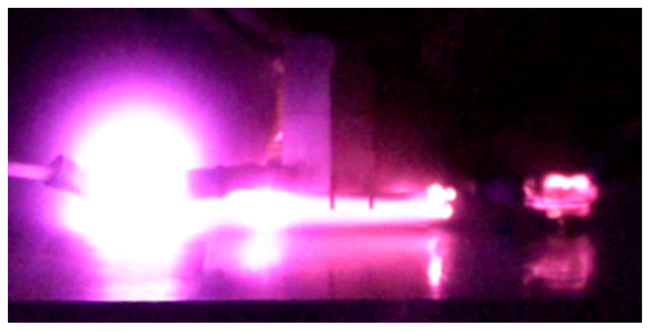
At the start of the test, the pressure inside the chamber is 10
3 mbar, the input voltage is measured at 600 V, and no current is flowing, indicating no current leakage or corona discharge. As the chamber begins to depressurize, due to the Paschen law, an electric arc occurs between the soldering joints of the primary and secondary winding within a pressure range between 0.8 mbar and 10 mbar, as observed in
Figure 11. In this range, the voltage source is operating in constant current mode, meaning a current leakage. Outside of this pressure range, no current leakage or corona effect has been observed in the transformer, suggesting that electrical isolation within the core is maintained.
Analyzing the effects observed under partial pressure conditions shows that the transformer, for final implementation, must be modified to prevent HV points from coming into contact with the atmosphere. Some potential solutions include applying an electrically insulating coating layer on exposed parts or using planar transformers.
The next step is to verify that the power cell can operate under high vacuum conditions (10
−4 mbar) using the experimental setup shown in
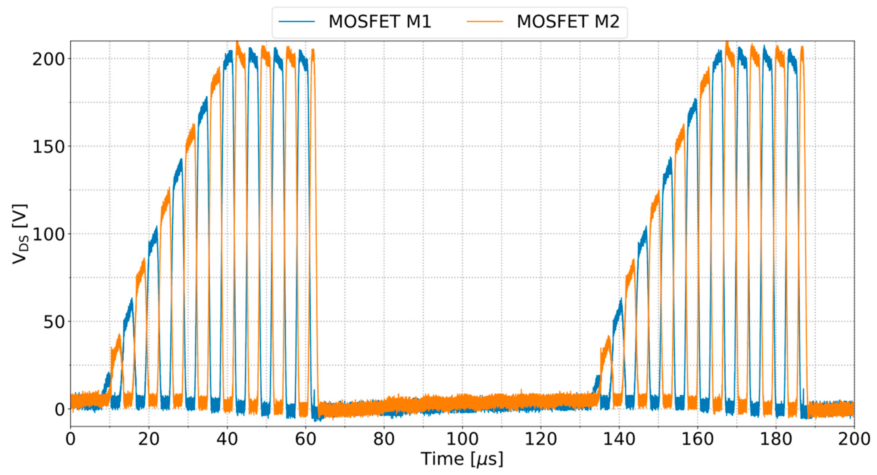
Figure 12. The vacuum chamber is depressurized to the desired pressure, and then the circuit is powered on. During operation, a constant output at 300 V has been observed. On the power cell, the V
DS of the DCX MOSFET is measured, and it is verified that ZVZC conditions are still maintained, as shown in
Figure 13. The waveforms observed are similar when operating under both ambient pressure and high vacuum conditions.
Using the same setup as in
Figure 12, a decompression in the vacuum chamber was performed from 10
3 mbar to 10
−3 mbar with the converter powered on. During rectification, a reverse voltage of 600 V exists between the terminals of the diode. At 3 mbar, a corona discharge appeared between the pair of rectifier diodes until it stabilized in only one of them, as observed in
Figure 14. At this pressure, the solar array simulator operates normally, with no faults detected on the primary side, thanks to the galvanic isolation. Power is transferred from the primary to the secondary; however, almost no current flows to the load due to the current discharge occurring between the diodes.
Typical solutions to prevent a corona discharge between the terminals of the rectifier diodes include applying an electrically insulating coating layer to the electric components on the secondary side of the power cell or encapsulating via a potting the entire power cell. While potting ensures excellent electrical isolation, it comes with a significant trade-off in terms of increased weight and reduced thermal dissipation.
5. Results Discussion
Increasing the Technology Readiness Level (TRL) requires overcoming some technological challenges, yet it also presents advantages over alternative solutions. The S3DCX topology is based on two common techniques used in space applications, which simplifies reliability studies at the system level. However, the main obstacle is the lack of rad-hard SiC Schottky diodes for HV in space.
High-power space platforms that require HV distribution buses are still under development. Nowadays, a significant debate is whether to implement a single HV distribution bus or a dual bus architecture composed of a low-voltage bus to power most of the satellite systems and an HV bus dedicated to high-power payloads and electric propulsion. The dual-bus approach allows the HV bus to be deactivated during LEOP, a scenario characterized by partial pressure conditions, thus reducing the requirements for electrical isolation. However, this approach increases the overall complexity of the architecture. On the other hand, the single bus architecture is simpler in comparison, but increased efforts are needed to provide electric isolation on the HV component to prevent corona effects during LEOP operations.
The experimental implementation of the S3DCX employs 300 V power cell modules rated at 400 W, with serialization needed to achieve 600 V and 900 V distribution buses. The laboratory prototype requires a significant number of modules to handle the power processing for the HV distribution bus. Therefore, increasing power density is crucial to reduce the number of modules required and, in the process, eliminate the need to serialize power cells for HV buses. To achieve this, two methods can be explored, both requiring further development.
The first method involves increasing the voltage from the solar arrays to 300 V, removing the need to serialize for 900 V distribution bus at a transformation gain of 1:3. However, increasing the solar array voltages above 120 V introduces the risk of appearing electric arcs between the solar cells and slip rings, needing arc mitigation methods [
8]. The second method, achieved by maintaining 100 V solar arrays, involves increasing the DCX transformation ratio to 1:6 and 1:9, with only one power cell required to achieve the 600 V and 900 V distribution bus. Both methods require an increase in the voltage rating and reliability for components such as MOSFETs, diodes, capacitors, and the electric isolation of the transformer.


