1. Introduction
Satellite development has been rapidly increasing worldwide with the emergence of new space trends in the space industry. Small satellites that can be developed in a short period at a low cost are emerging as economical space programs [
1]. One of the key factors in developing cost-effective small satellites is reducing the mass and volume of the satellite payload, much of which comprises electronics. Therefore, the weight reduction of electronics is a crucial issue, considering the stowage efficiency of the launch vehicle and launch costs. To reduce the weight of electronics, a highly reliable structural design methodology for spaceborne electronics based on accurate evaluation is required to prevent overdesign.
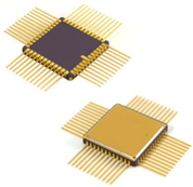
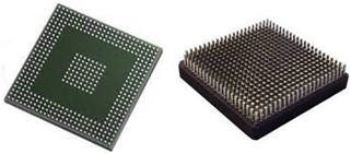
Spaceborne electronics on satellites experience various extreme environmental loads during launch vehicle liftoff [
2]. These dynamic loads are induced over a wide frequency range via propellant dispensing, impact with the atmosphere, and shock from the multistage separation of the launch vehicle. Among these loads, electronics are particularly prone to fatigue damage at package solder joints. To actualize advanced satellite missions, highly integrated electronic packages, such as ball grid arrays (BGAs) and column grid arrays (CGAs), have been applied in recent years to enhance the functionality and performance of electronics. However, these highly integrated electronics are known to be more susceptible to fatigue failure in a random vibration environment than previously developed packages, such as dual in-line and pin grid array packages [
3]. Therefore, a highly reliable structural design methodology for electronics is essential for successful satellite missions.
Conventionally, the structural safety of solder joints in a launch vibration environment has been evaluated based on Steinberg’s fatigue failure theory [
3] developed in the 1970s. This theory suggests that if the maximum behavioral displacement of the printed circuit board (PCB) is designed to be below the allowable displacement calculated using the empirical formula, the solder joint can guarantee a fatigue life of more than 20 × 10
6 cycles under a random vibration environment. With regard to the modeling and simulation of PCB based on this theory, it is possible to estimate a relatively accurate board displacement without detailed FE (finite element) modeling of the electronic package, even with insufficient modeling using only rigid link elements [
4,
5]. Based on this advantage, previous studies have evaluated the structural safety of electronics by establishing FE models using Steinberg’s theory to perform structural analyses [
4,
6,
7,
8].
However, recent studies have reported that the allowable displacements estimated using the empirical formula of Steinberg’s theory have limitations regarding the prerequisite of having a simple half-sine mode shape at the center of a simply supported rectangular PCB [
9]. This means that it is difficult to apply this theory to PCBs with complex mode shapes owing to their asymmetrical shapes, irregular fixation point locations, and reinforcement applications. Accordingly, an overly positive or negative margin can be derived when calculating
MoS because of the conditions assumed in Steinberg’s theory, resulting in an evaluation result with low reliability. Despite these disadvantages, Steinberg’s theory is still used to evaluate spaceborne electronics because no alternative solution currently exists.
To overcome the limitations of Steinberg’s theory, Park et al. [
10] proposed the Oh–Park methodology to evaluate the structural safety of spaceborne electronics with solder joints based on the critical-strain theory. The key approach is to evaluate the structural safety of solder joints for random launch vibrations based on
MoS calculations concerning the PCB strain. This approach enables mitigating the issues related to Steinberg’s theory, such as unreliable structural safety evaluations and the possibility of structural overdesign.
Park et al. [
10,
11] proposed simplified FE modeling techniques for BGAs, CGAs, and small-outline packages (SOPs), which consist only of zero-dimensional (0D) lumped mass and rigid link elements. These techniques have been effective in reducing the time and effort required to model the packages and are reasonably valid for evaluating the structural safety of the solder joint. For evaluating the effectiveness of the Oh–Park methodology, the above package specimens with various boundary conditions of PCBs were fabricated and exposed to random vibration excitation. By comparing the
MoS of solder joints and
TTF of tested specimens, Park et al. [
10,
11] proved that their proposed methodology represented the test results well, in contrast to Steinberg’s theory, which showed invalid results for most of the specimen cases.
In previous studies [
10,
11], the Oh–Park methodology was validated only for a single package mounted on PCB specimens without a housing structure. However, in the actual electronics design, various types of electronic packages were mounted on PCBs, which were assembled in the mechanical housing of the electronics. In this case, the elastic vibration modes of the housing structure and irregular and complex modes of the PCB affected the fatigue life of the solder joints of the packages. To demonstrate whether the proposed design methodology is effective in the actual design of spaceborne electronics, it is necessary to verify the effectiveness of the theory under conditions similar to those of actual electronics, not the single PCB specimens used in previous research.
In this study, to validate the effectiveness of the Oh–Park methodology from an actual design perspective, an integrated test specimen of electronics, where a PCB with various boundary conditions of eight sample packages was mounted on mechanical housing structures, was fabricated and exposed to random vibration excitation on a vibration shaker. Using conventional Steinberg’s theory, the TTF values of the tested specimens were compared with the MoS values calculated using the Oh–Park methodology with simplified FE modeling techniques. Technical assessments of the test results indicated that the Oh–Park methodology based on critical-strain-based theory provides a reliable and rapid solution for the actual design of electronics.
The remainder of this paper is organized as follows.
Section 2 describes the evaluation of Steinberg’s theory and the Oh–Park methodology.
Section 3 describes the design of the integrated comprehensive test specimen for electronics. and presents the results of the random vibration tests.
Section 4 compares the effectiveness of the proposed methodology with that of conventional Steinberg’s theory.
Section 5 concludes the paper.
2. Structural Design Methodology
Steinberg’s theory, developed in the 1970s, has been widely used to evaluate the structural safety of electronic package solder joints in a launch-random vibration environment during the development of conventional spaceborne electronics. This theory proposed the allowable PCB displacement,
, which is empirically calculated as follows:
where
C is a constant for various types of electronic packages,
t is the thickness of the PCB,
L is the length of the package,
r is the relative position coefficient of the package mounted on the PCB, and
B is the length of the PCB parallel to the package. Using Equation (1), the
MoS of a solder joint relative to the criteria presented in Steinberg’s theory is calculated as follows:
where
SF (safety factor) is the safety factor of the
MoS.
values of 1.11, 1.25, and 1.4 have been used for
MoS calculations in previous studies [
4,
6,
7,
8]. Applying
values to stress provides the
in terms of fatigue life in accordance with the stress–life cycle curve (
-
curve) described below [
12]:
where
is the fatigue exponent of the solder or lead-frame material of the package. Steinberg [
3] assumed that the stress or strain of a solder joint was proportional to board displacement (
). Therefore, the relationship above is valid for
, as described in Equation (3). In general, Sn-Pb37 solder materials are widely used in the electronic packages of spaceborne electronics. The value of
for Sn-Pb37 solder materials, which are widely used in the electronic packages of spaceborne electronics, is 6.4 for high-cycle fatigue, such as vibration [
3]. The European Cooperation for Space Standardization (ECSS) rules [
13] recommend using an
(factor of safety) of 4.0 or higher for fatigue. For example, if Sn-Pb37 solder is used for the package, the corresponding
on
becomes approximately 1.25, according to Equation (3) [
11]. These aspects were reflected to determine
in evaluating the solder joint safety for the selected comprehensive specimen, as described later.
However, because of the above empirical formula, Steinberg’s theory has theoretical limitations in evaluating spaceborne electronics because it assumes a simple-support rectangular PCB with an ideal half-sine mode shape [
3]. Accordingly, when the mode shape of the PCB board becomes complex owing to the asymmetrical shape, irregular constraint point location, and application of stiffeners, an error occurs in the calculated
because it deviates from Steinberg’s assumption. In particular, the factor
r is the main source of calculation error because
can be overestimated as the electronic package mounting location approaches the edge of the PCB board. Accordingly, if the PCB exhibits a non-half-sine mode, the values of
B and
r in Equation (1) become ambiguous, leading to inaccurate results such as an excessively positive or negative evaluation of the fatigue life of solder joints compared with the actual fatigue life. Furthermore, when evaluating based on board displacement using Steinberg’s theory, the local strain effect acting on the package owing to the presence of adjacent packages, connectors, or mechanical fasteners is ignored. Despite these limitations, Steinberg’s theory is still being applied to the design and evaluation of spaceborne electronics.
To overcome the theoretical limitations of Steinberg’s theory, Park et al. [
10] proposed the critical-strain-theory-based Oh–Park methodology as a structural design methodology for evaluating the structural safety of solder joints in spaceborne electronics. This methodology evaluates the structural safety of solder joints in a manner similar to Steinberg’s theory; however, the
MoS is calculated based on the PCB strain. The critical value
of the in-plane principal strain of the PCB for the package is estimated using the modified formula from Equation (1) as follows:
where
C and
L are the same as those in Equation (1).
is the allowable in-plane principal PCB strain and is a major factor that can overcome the theoretical limitations of Steinberg’s theory by replacing factors
r and
d in Equation (1).
is calculated as follows:
where
is analytically estimated by considering the derivative of
as the strain rate of the PCB, and
and
are derived as follows:
where
and
are the RMS in-plane normal strains and
is the RMS in-plane shear strain. To meet 20 × 10
6 cycles, which is the solder joint survival criterion in a random vibration environment, the
MoS for the PCB board strain is calculated as follows:
This approach can evaluate the structural safety of the electronic package solder joint with high reliability compared with Steinberg’s theory, which can cause structural overdesign owing to the abovementioned limitations. Moreover, this methodology has been experimentally validated through a fatigue-life test by fabricating a PCB board on which a single electronic package with various boundary conditions was mounted [
10,
11].
To validate this methodology, Park et al. [
10] evaluated the structural safety of the electronic package solder joint by performing structural analysis using simplified FE modeling, and the package was modeled using a 0D lumped mass and a rigid link element to simulate the package body and solder joints, respectively. This modeling technique has the advantage of being useful when many trade-off studies are required to verify the structural design of spaceborne electronics in the initial design phase, as it can save considerable time and effort compared to the conventionally used detailed FE modeling technique. Park et al. [
10,
11] validated a simplified FE modeling technique for BGA, CGA, and SOP packages and performed a trade-off study by varying the number of nodes on the PCB connected to the 0D lumped mass with a rigid link element to determine the most feasible modeling technique considering the solder joint characteristics of each device during validation. The tradeoff results are summarized in
Table 1. Furthermore, the validation of the simplified FE modeling technique yielded prediction results similar to those of the detailed FE modeling technique, and it was found that the structural safety of the solder joint can be predicted stably and quickly compared to Steinberg’s theory.
However, conventional validation of this methodology has only demonstrated its effectiveness when a rectangular PCB is bolted at regular distances and only a single electronic package is mounted. Under these conditions, the fundamental-mode response of the PCB indicated a simple shape, with the highest response at the center of the PCB and a lower response at the edges. Additionally, when designing actual spaceborne electronics, the PCB and electronic package are structurally affected by the vibration response characteristics of the housing structure that protects the PCB; therefore, this must be considered. Therefore, if the PCB specimen test results were obtained under conditions that exhibited complex mode shapes under the influence of the vibration response behavior of the housing structure, the validity of the methodology can be proven under more realistic conditions. For this reason, in this study, the effectiveness of the methodology was demonstrated in terms of the actual design through a fatigue-life test by mounting a PCB with eight electronic packages under various boundary conditions on a housing structure and exposing it to a random vibration environment.
3. Fatigue-Life Test of Comprehensive Specimens
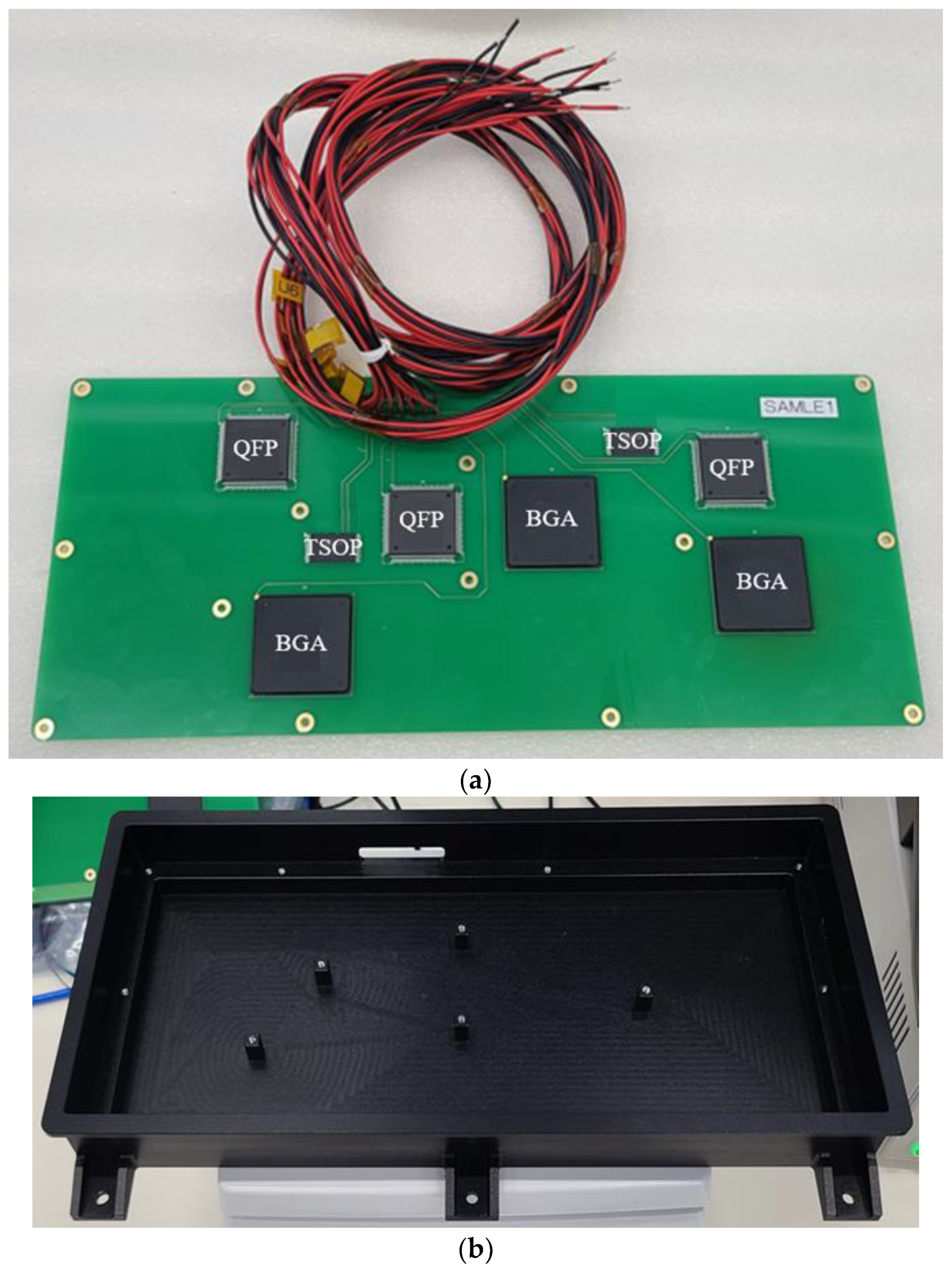
To verify the effectiveness of the Oh–Park methodology in actual conditions where the PCB is combined with a mechanical housing and the elastic mode of the housing is affected, housing structures and PCB specimens with various mounted electronic packages were designed and fabricated, as shown in
Figure 1. The PCB was made of an FR-4 laminate with an area of 150
350 mm and thickness of 1.6 mm. The weight of the PCB on which the package was mounted was 243.5 g. For the PCB specimen, more realistic conditions were achieved by intentionally designing non-uniform positions of the package and peripheral fastening parts. Eight packages, PBGA (3 EA), TSOP (2 EA), and QFP (3 EA), were mounted on the PCB specimens; the specifications of these packages are summarized in
Table 2. The above three types of electronic packages were selected because the probability of failure is relatively high, because the structural configuration of the solder joint and the size of the package are generally large among the various package types used in designing actual electronics. Unlike general packages with electrical functions, these are dummy test packages with a daisy-chain circuit in which all solder joint pins are connected in series to detect cracking in the solder joint by monitoring the circuit resistance variation in the test. The PCB specimen was fastened to mechanical housing made of aluminum-6061, which was 370 × 206 × 30 mm in size and 1080 g in weight.
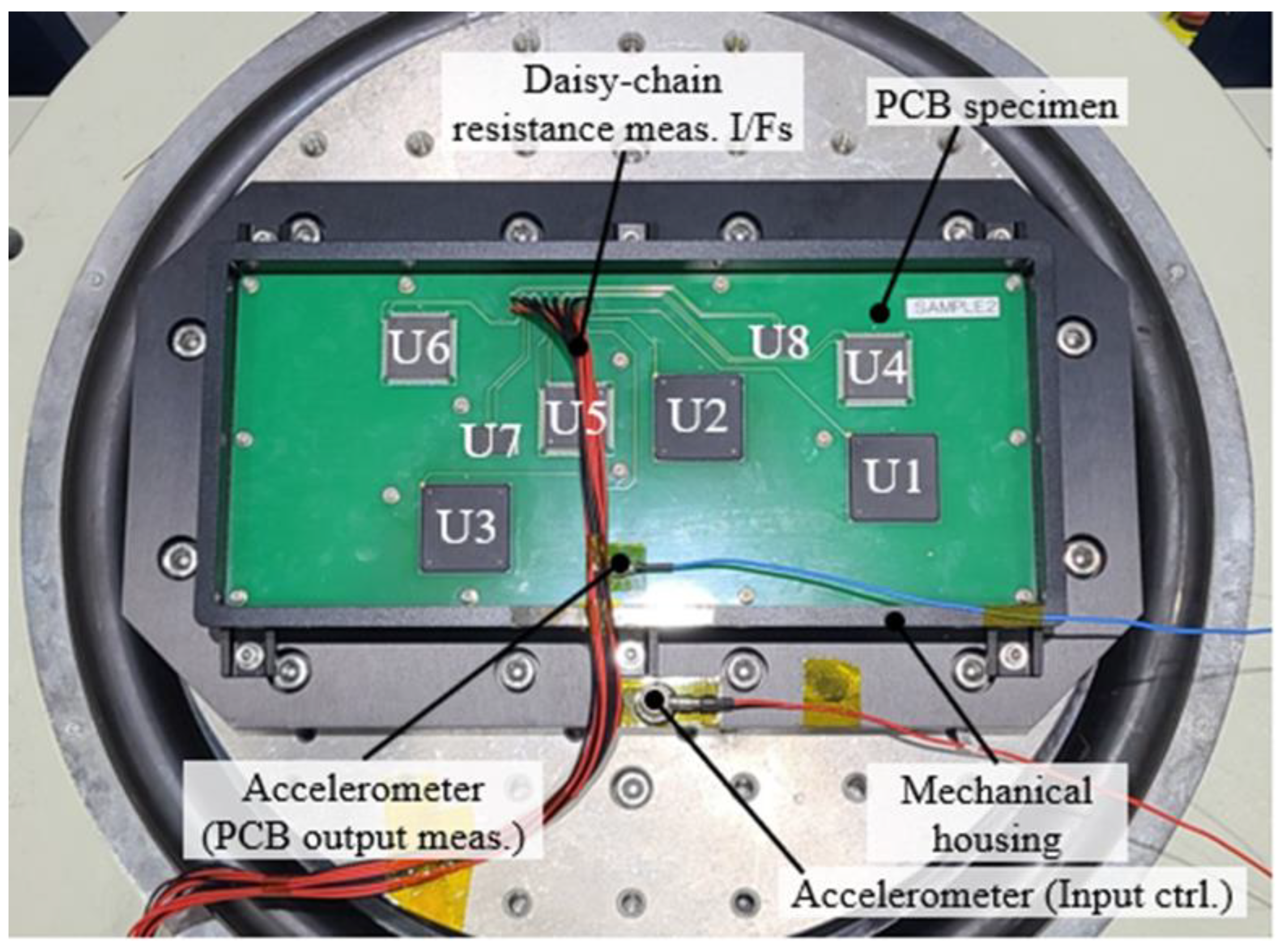
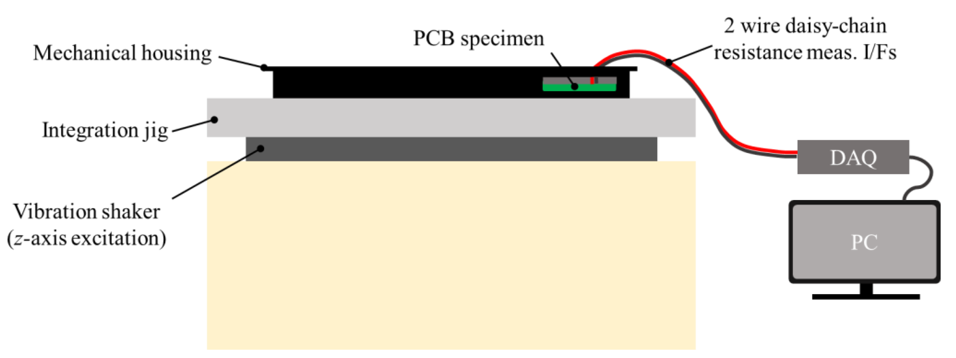
Figure 2 and
Figure 3 show the fatigue-life test setup for a comprehensive PCB specimen mounted on a vibration shaker and a schematic diagram of the setup, respectively. The test was performed such that a random vibration of 20 grms, as specified in
Table 3, was continuously excited until the electronic package solder joint failure criterion was reached. To determine the solder joint failure during the test, the above-described two-wire resistance was measured for each electronic package using a data acquisition device (DAQ) DAQ6510 (Keithley Co. Ltd., Cleveland, OH, USA). Here, the measurement accuracy of the DAQ was set to less than 10
−2 Ω, and the sampling rate was set to 1.7 sample/s. Moreover, based on the IPC-9701A standard, the solder joint failure criterion was set when during the test, the DAQ detected five times in a row a resistance value that was 20% higher than the initial value [
18].
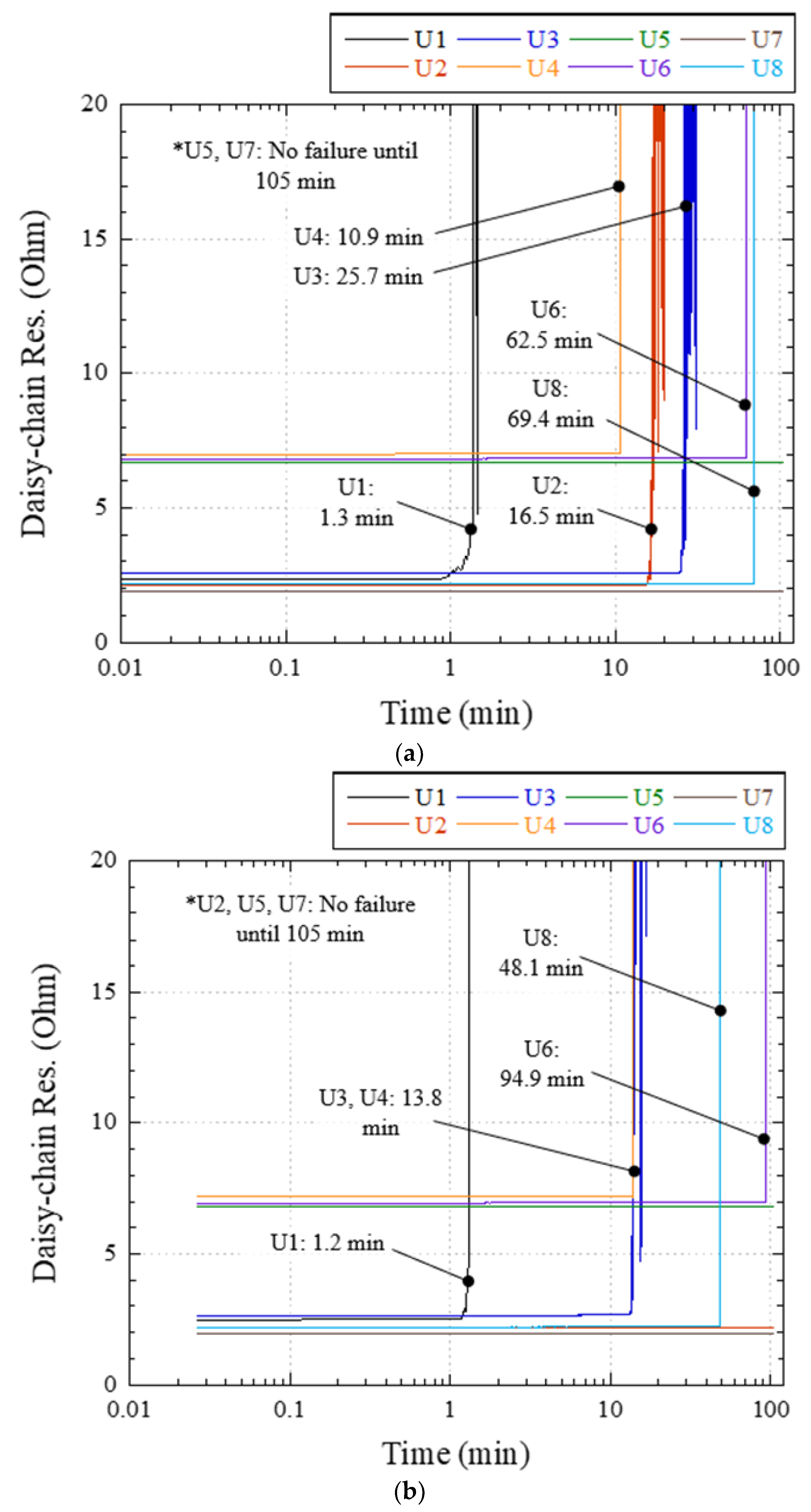
Figure 4a,b show the daisy-chain resistance time history for each sample, and
Table 4 summarizes the
TTF values for each package. In the test, the U4 package failed after the U1 package reached the failure criterion for the first time, after which packages U3, U6, and U8 failed. For the U2 package, there was no failure in Sample 2, unlike in Sample 1. As shown in the above results, the deviation in the
TTF results of the solder joint for each electronic package is due to the influence of the production tolerance of the electronic package and solder joint and to the manufacturing/assembly tolerances of the PCB and mechanical housing structure, although the specimens of the same configuration are manufactured via the same process. Particularly, tolerance may occur during assembly, such as when the PCB board is placed in the center of the screw–tap interface of the mechanical housing and twisting of the PCB during bolt-torque application. Finally, no sample failed in packages U5 and U7, and the above test results were used to validate the Oh–Park methodology for a comprehensive PCB specimen with multiple packages mounted under different boundary conditions.
4. Verification of Structural Design Methodology
To validate the Oh–Park methodology for comprehensive PCB specimens, an FE model was established based on the simplified FE modeling technique proposed by Park et al. [
10], and a structural analysis was performed. The structural safety of various packages was evaluated based on the results of the fatigue-life test described in
Section 3, and a comparative analysis between the Oh–Park methodology and Steinberg’s theory was also performed.
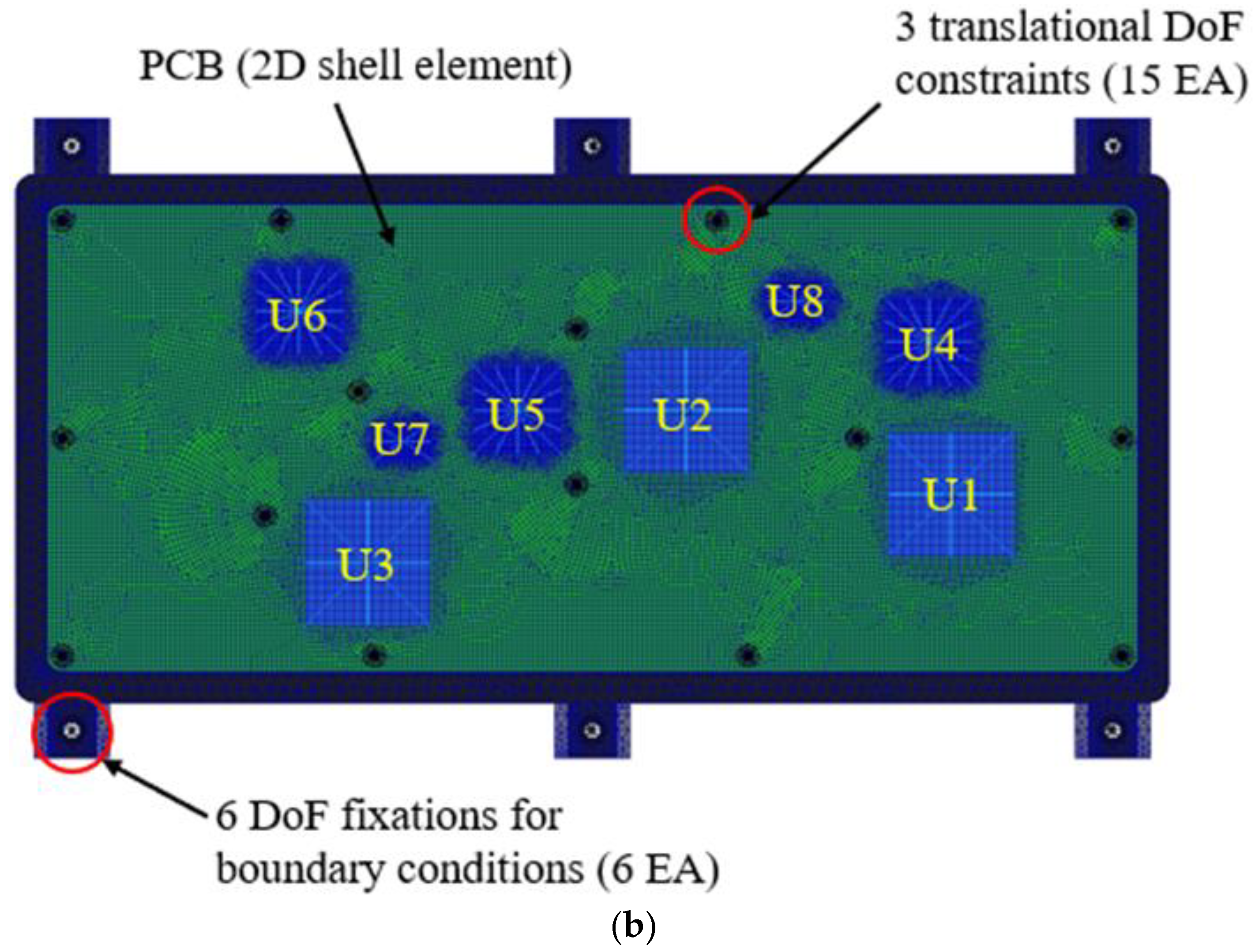
Figure 5a,b show details of the configuration of each electronic package and FE model for the mechanical housing and comprehensive PCB specimens, respectively.
Table 5 and
Table 6 provide detailed summaries of the specifications and material properties of the FE model, respectively. The mechanical housing was modeled using a solid element (tet 10), and six-degree-of-freedom (
DoF) constraints were applied to the independent nodes of the rigid link elements for the outer six joints of the housing, which are boundary conditions.
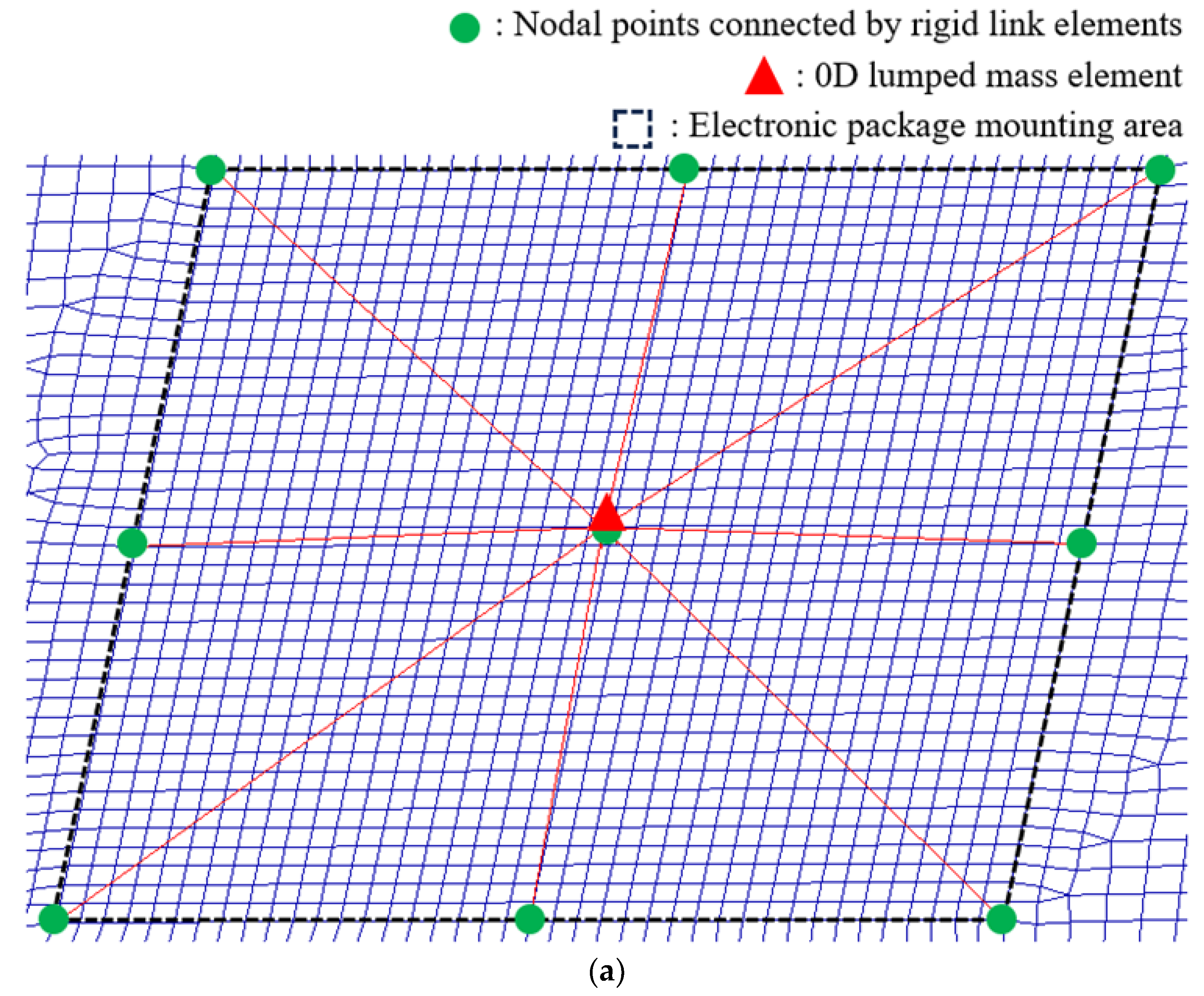
Figure 6a shows the guidelines for a simplified FE modeling technique for PCB and electronic packages (BGA). Moreover,
Figure 6b,c show representative examples of simplified FE models of a PCB with QFP and SOP packages, respectively. The PCB was modeled using shell elements (QUAD4, Tria3), which are more efficient in predicting the in-plane deformation for a flat structure such as a PCB than a solid element in terms of minimizing the mesh density. Because no rotational
DoF is provided, there is an advantage in that more accurate board strain results can be provided compared with solid elements, where stiffness can be overestimated. Moreover, a technique for determining the appropriate size of the shell element is essential to alleviate the overestimation problem because the board strain can be overestimated when the element is constrained by a rigid link [
10]. Accordingly, Park et al. [
10] developed a mesh modeling method capable of reasonable strain estimation method and applied it in their study as follows. The PCB area occupied by the electronic package body was uniformly meshed, and the mesh size was equivalent to the package body length divided by the number of solder balls or leads on one side of the package. The remaining PCB board area was meshed to 1.5 mm. The rigid link elements used to simulate bolted joints in packages and PCBs were constrained to only three translational
DoFs. Electronic package FE modeling was established based on the 0D lumped mass and rigid link elements presented in previous studies [
10,
11]. This is one of the simplest modeling techniques and has a significant advantage in terms of saving time and effort in constructing a finite element model. Furthermore, a feasible modeling technique was found, as presented in
Table 1, through a trial-and-error method based on numerous structural analyses of various packages in previous studies, which were appropriately applied to each package in this study, as shown in
Figure 6.
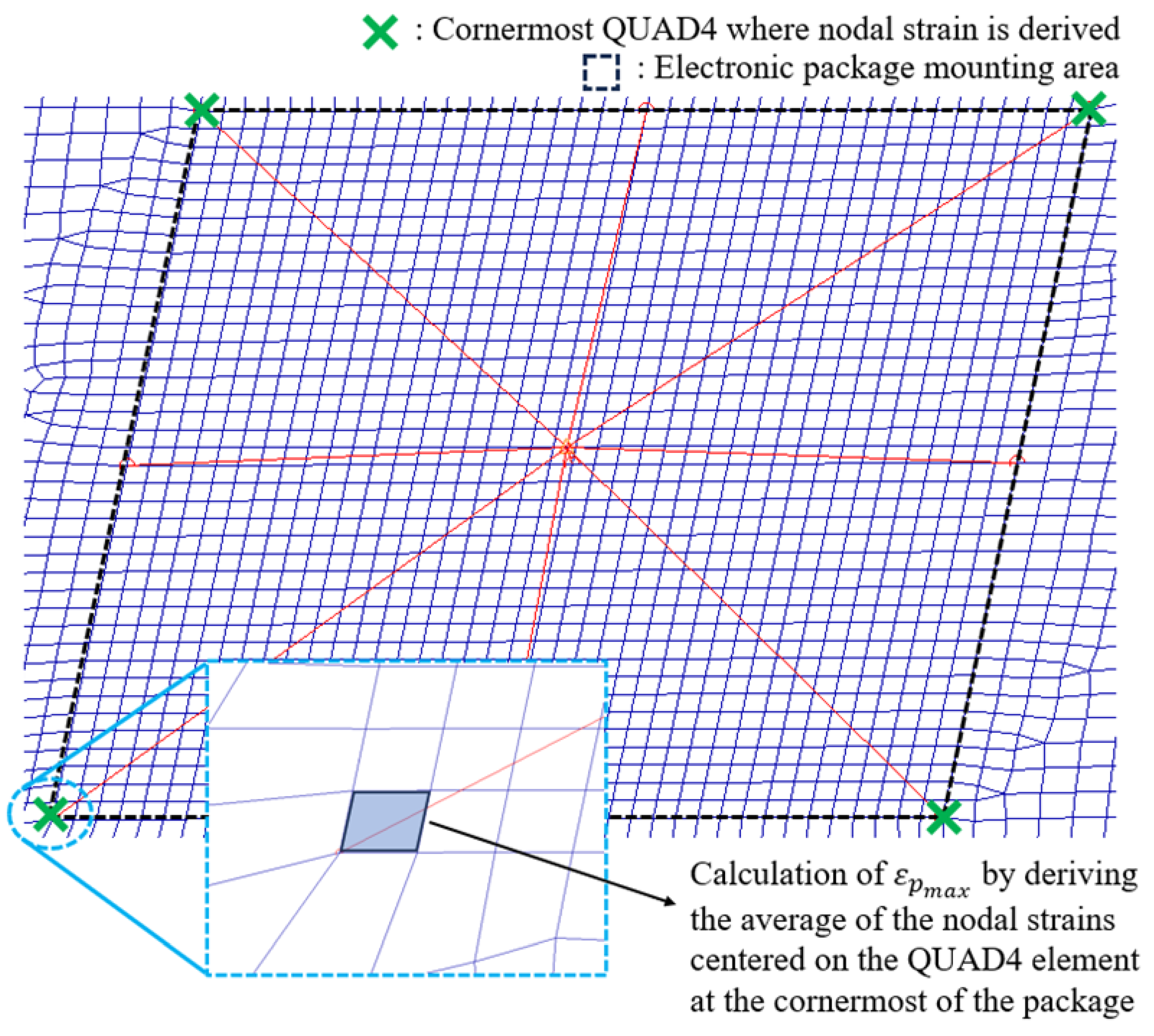
After performing random analysis based on the previously established FE modeling,
was derived from the RMS nodal strains extrapolated from the element centroid, as shown in
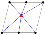
Figure 7, and it is the average of the strains of four nodes belonging to the most corner QUAD4 element in the package mounting area. All modeling and approaches presented in this study are also part of the Oh–Park methodology and were used to evaluate the structural safety of electronic package solder joints mounted on comprehensive specimens.
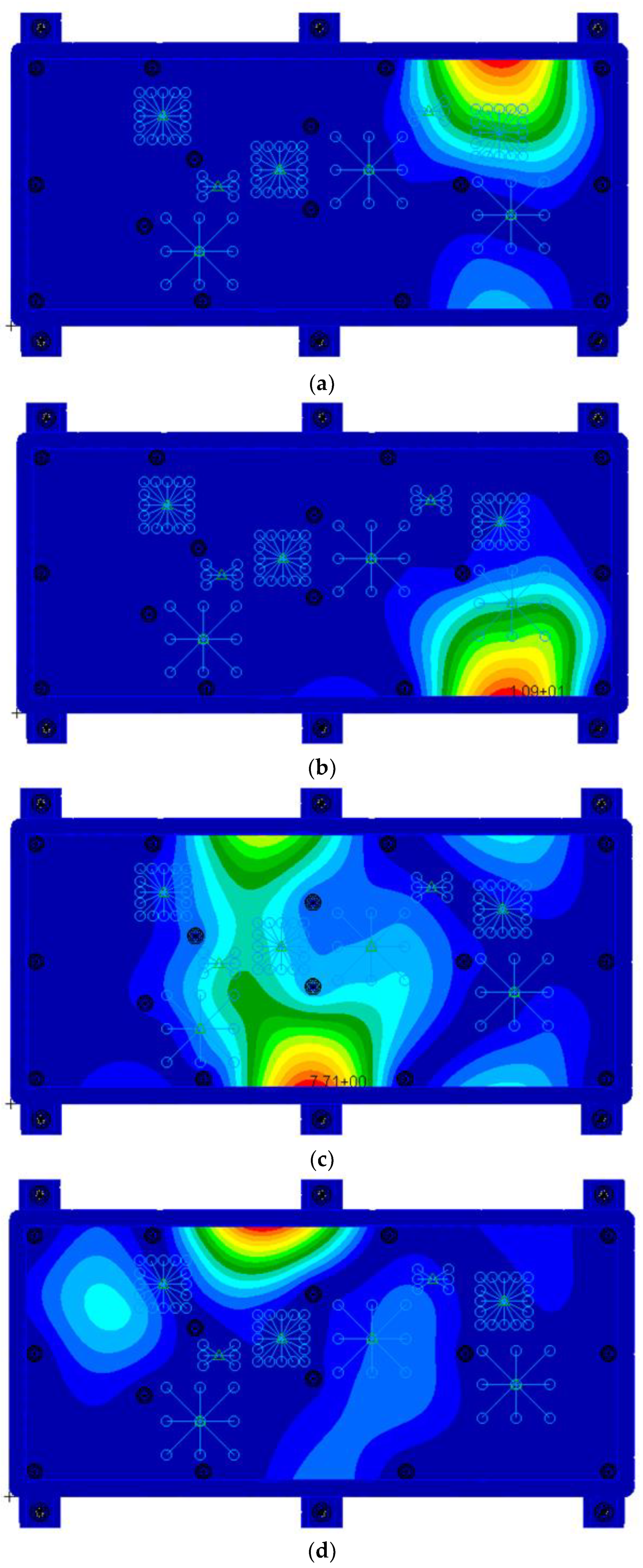
A modal analysis was performed on the constructed FE model, and the results are presented in
Figure 8 and
Table 7. The above results indicate that the location of the main resonance part on the PCB for each mode is different and that the fundamental mode that affects the mechanical load on the electronic package changes accordingly. Moreover, the mode shape indicates a complex shape due to the irregular fixation points, the location of the packages, and the influence of the housing behavior according to the design configuration of the comprehensive specimens. Generally, to satisfy various advanced requirements and design factors in the tradeoff design process of actual electronics, these complex mode shapes are often indicated by an increase in fixation points and the application of additional stiffeners. Based on the conditions under these mode shapes, a random analysis was performed to evaluate the structural safety of the solder joints for each package, and the results were compared with those of the fatigue-life test.
Table 8 summarizes the
MoS calculation results for the coefficients according to the electronic package type and PCB mode frequency for the eight electronic package types of the comprehensive specimen, as well as the results of the solder joint structural safety assessment derived from conventional Steinberg’s theory and the corresponding methodology. When analyzing Steinberg’s theory, the
MoS calculation is based on the relative displacement of the PCB excluding the displacement of the input from the absolute displacement value, and the condition definition of the allowable displacement formula considers only the displacement for the actual bending of the PCB. For the evaluation,
SF = 1.25 was selected and applied in the
MoS calculation for QFP208 and TSOP48 comprising a Sn-Pb37 solder and copper lead frame with
b = 6.4, according to the relationship described in Equation (3). Furthermore, the fatigue exponent (
b) of SAC305, a solder material of PBGA924, is 7.8, and
FoS is derived as 5.4 when calculated using Equation (3). As this is greater than
FoS = 4.0, which is the ECSS standard recommended criterion, PBGA924 was evaluated at
SF = 1.25, similarly to the other packages. In the Oh–Park methodology,
was used to calculate
MoS by deriving it through Equation (6) based on the modal and random analysis results and substituting it into Equation (5). As a result of the evaluation, the
MoS value calculated using Steinberg’s theory generally shows a positive margin from a minimum of 1.43 to a maximum of 85.65. However, the
MoS value for the allowable displacement was overly positive as all packages, except U5 and U7, failed in the actual test. In particular, in the case of U3, U5, and U6, which are located at the point where the dynamic response occurs in the 3rd mode where the PCB is affected by the elastic mode of the housing, it is observed that the
MoS difference reaches 59.9 times compared to other devices. This phenomenon is caused by the uncertainty of the calculation results owing to the ambiguous boundary conditions for calculating the allowable displacement when applying Steinberg’s theory. This leads to excessively positive results under these conditions and indicates a low-reliability evaluation result.
However, when the structural safety of solder joints was evaluated using the critical-strain-based Oh–Park methodology, negative margins were derived in all electronic packages, and the MoS judgment results reasonably represented the actual fatigue-life test results compared with Steinberg’s theory. Here, some packages showed a negative margin, although no failure occurred during the test. This is because the damage to the solder joint gradually progressed according to the continuous random vibration excitation in the actual test, and the strain response propagating to the surrounding packages was gradually relieved. This is determined to be affected by parts that are difficult to reflect in the analysis, such as changes in circumstances and boundary conditions. Additionally, because the structural safety of spaceborne electronics in a vibration environment is generally premised on ensuring the structural safety of all electronic packages and components, it is important to accurately identify the point and time of the electronic package where the first failure occurs, except in special cases, to ensure the MoS for it. Therefore, from this aspect, the results of the evaluation using the Oh–Park methodology demonstrate that a reasonable structural safety evaluation is feasible compared to Steinberg’s theory, even in a situation where electronic packages are mounted with various boundary conditions and the PCB is affected by the elastic mode of the mechanical housing.


