Dual-Mode FPGA-Based Triple-TDC With Real-Time Calibration and a Triple Modular Redundancy Scheme


Abstract
1. Introduction
2. Proposed FPGA-Based Triple-TDC
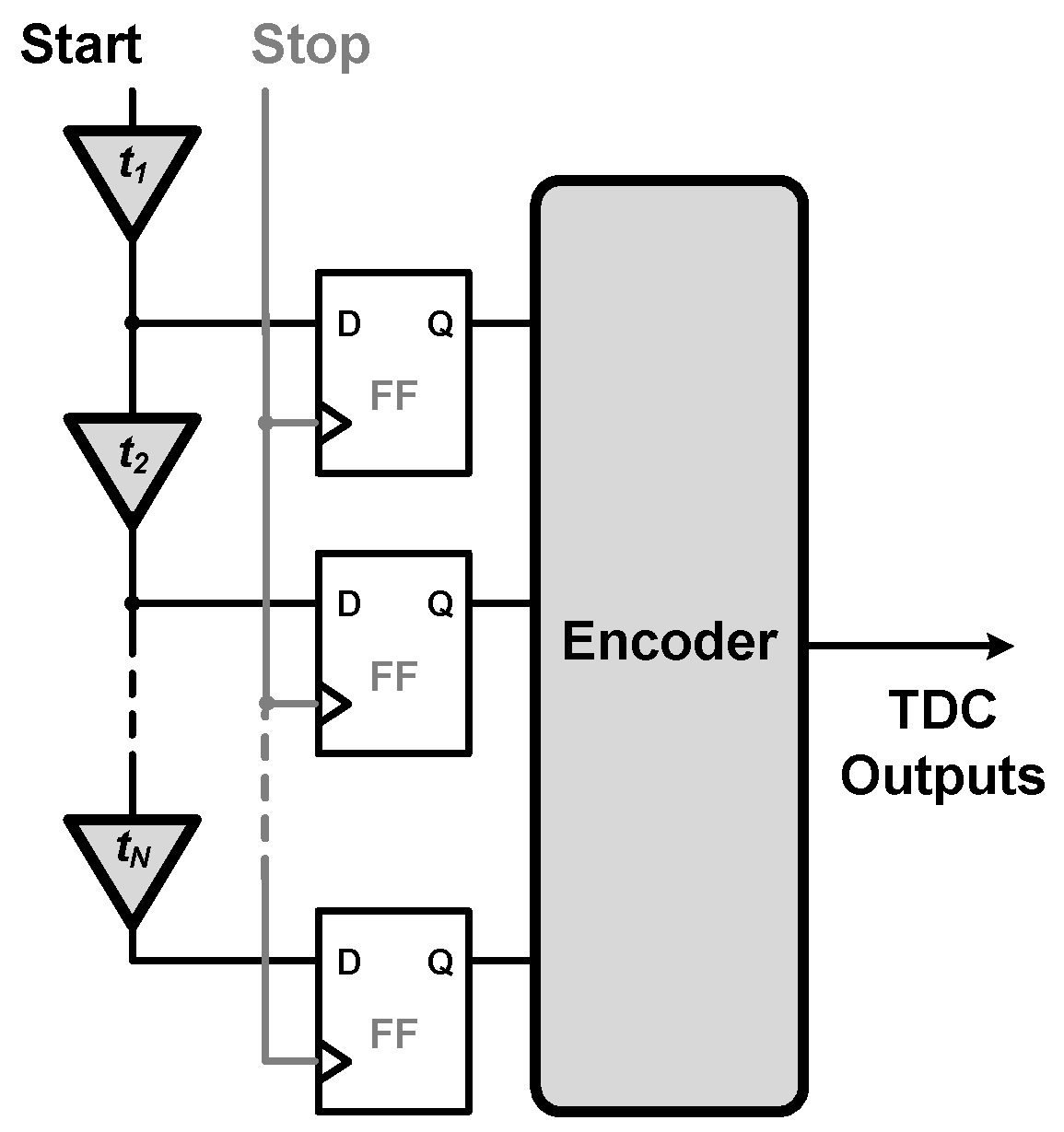
2.1. Tapped Delay Line TDC
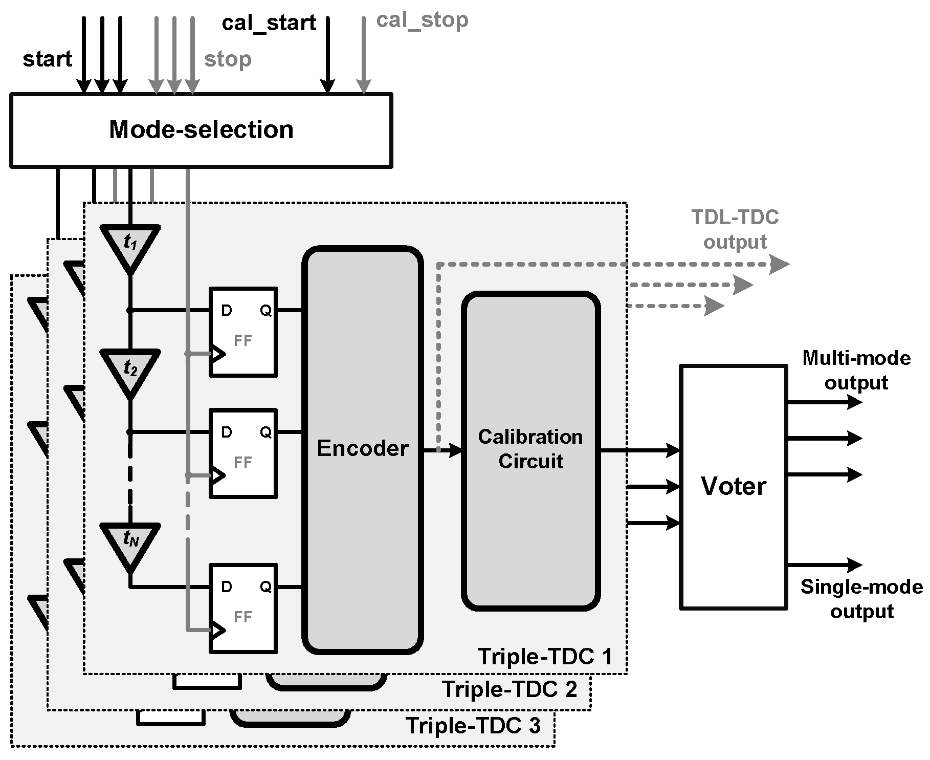
2.2. Proposed Triple-TDC Design
- Three TDLs can be layout into different locations of a single FPGA chip, thus the diversity of the delay cell can improve the uncertainty of time delay with the TMR technology. The time resolution can be improved.
- The proposed triple-TDC provides dual operation modes for multi-channel and high-resolution applications.
- For the high-resolution application (single-mode), three-fold resources are used to improve the resolution. The resources overhead include area, power, and speed.
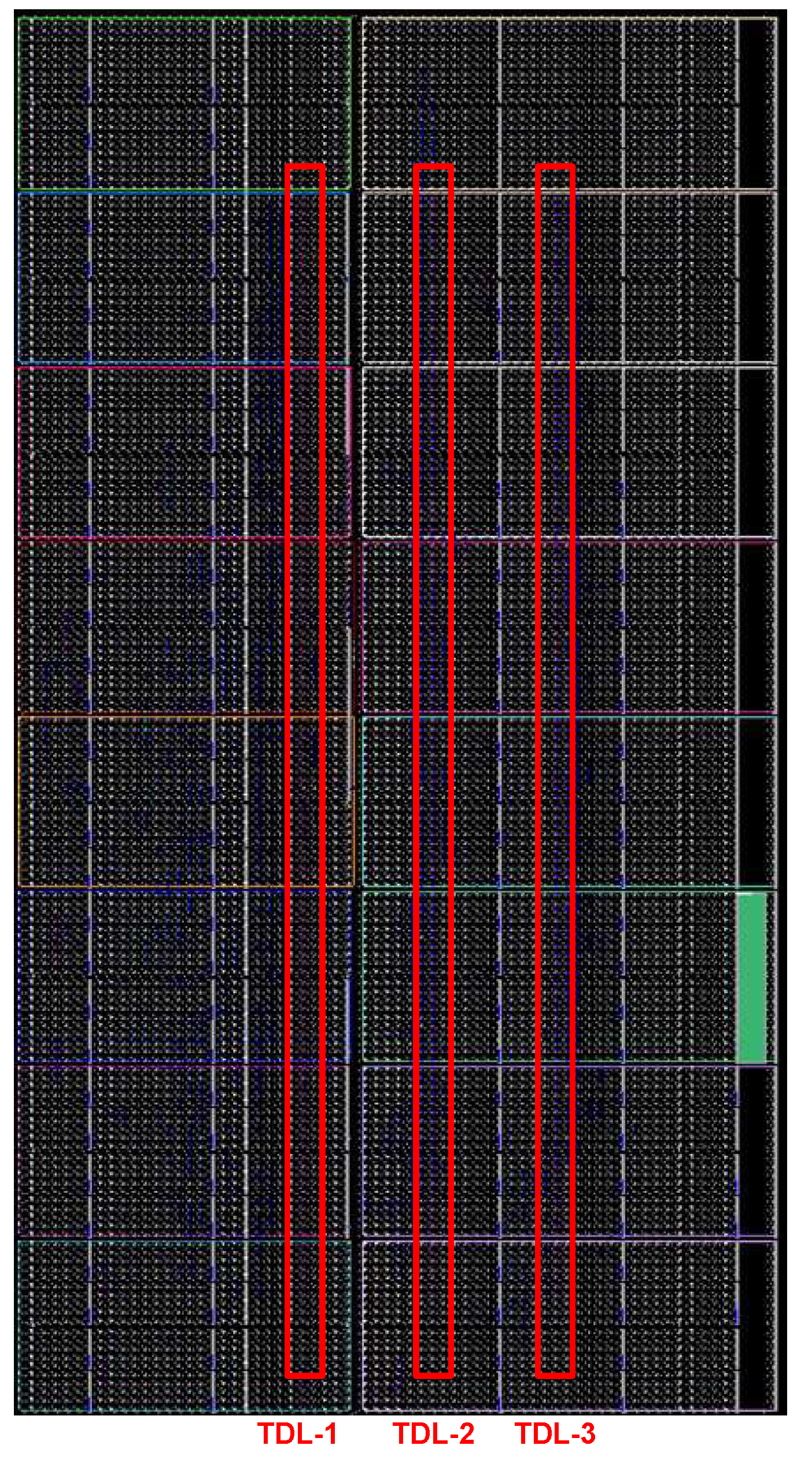
2.3. Triple-TDC Implementation
3. Experimental Results and Discussion
3.1. Experimental Setup
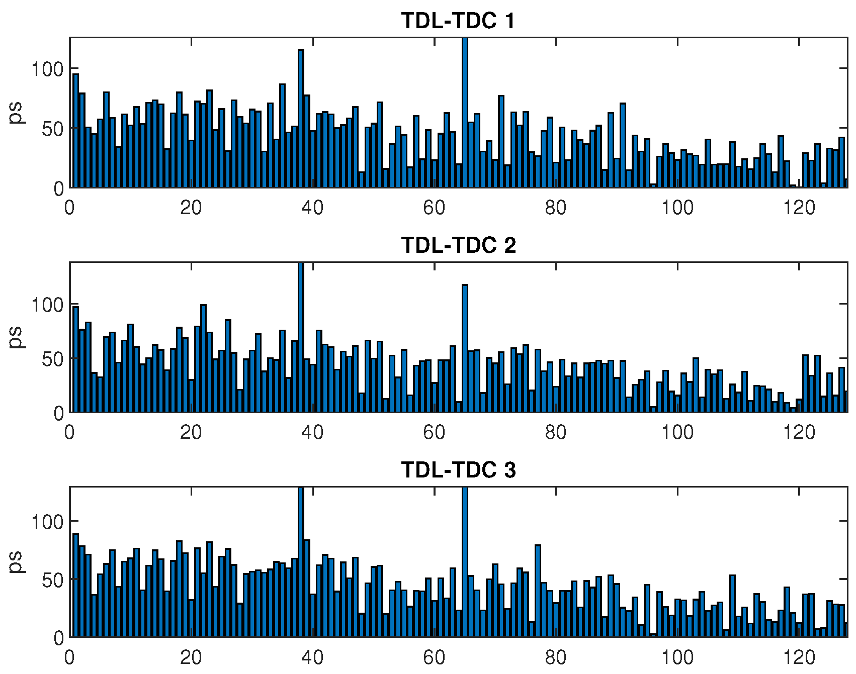
3.2. Experimental Results
4. Conclusions
Funding
Acknowledgments
Conflicts of Interest
References
- Chen, Z.; Shi, W.; Xiong, G.; Yang, J.; Xu, Y. A 63.3ps TDC Measurement System Based on FPGA for Pulsed Laser Ranging. In Proceedings of the 2019 IEEE 13th International Conference on ASIC (ASICON), Chongqing, China, 29 October–1 November 2019; pp. 1–4. [Google Scholar]
- Garzetti, F.; Lusardi, N.; Geraci, A.; Dobovicnik, E.; Cautero, G.; Dri, C.; Sergo, R.; Stebel, L. Fully FPGA-based and all-reconfigurable TDC for 3D (X, Y, t) Cross Delay-Line detectors. In Proceedings of the 2018 IEEE Nuclear Science Symposium and Medical Imaging Conference Proceedings (NSS/MIC), Sydney, Australia, 10–17 November 2018; pp. 1–3. [Google Scholar]
- Arabul, E.; Paesani, S.; Tancock, S.; Rarity, J.; Dahnoun, N. A Precise High Count-Rate FPGA Based Multi-Channel Coincidence Counting System for Quantum Photonics Applications. IEEE Photonics J. 2020, 12, 1–14. [Google Scholar] [CrossRef]
- Moses, W.W.; Buckley, S.; Vu, C.; Peng, Q.; Pavlov, N.; Choong, W.; Wu, J.; Jackson, C. OpenPET: A Flexible Electronics System for Radiotracer Imaging. IEEE Trans. Nucl. Sci. 2010, 57, 2532–2537. [Google Scholar] [CrossRef]
- Sportelli, G.; Belcari, N.; Guerra, P.; Spinella, F.; Franchi, G.; Attanasi, F.; Moehrs, S.; Rosso, V.; Santos, A.; Del Guerra, A. Reprogrammable Acquisition Architecture for Dedicated Positron Emission Tomography. IEEE Trans. Nucl. Sci. 2011, 58, 695–702. [Google Scholar] [CrossRef]
- Yousif, A.S.; Haslett, J.W. A Fine Resolution TDC Architecture for Next Generation PET Imaging. IEEE Trans. Nucl. Sci. 2007, 54, 1574–1582. [Google Scholar] [CrossRef]
- Junnarkar, S.S.; O’Connor, P.; Vaska, P.; Fontaine, R. FPGA-Based Self-Calibrating Time-to-Digital Converter for Time-of-Flight Experiments. IEEE Trans. Nucl. Sci. 2009, 56, 2374–2379. [Google Scholar] [CrossRef]
- Marino, N.; Baronti, F.; Fanucci, L.; Saponara, S.; Roncella, R.; Bisogni, M.G.; Guerra, A.D. A Multichannel and Compact Time to Digital Converter for Time of Flight Positron Emission Tomography. IEEE Trans. Nucl. Sci. 2015, 62, 814–823. [Google Scholar] [CrossRef]
- Aguilar, A.; Garcia-Olcina, R.; Leiva, I.; Martinez, P.A.; Martos, J.; Soret, J.; Suarez, A.; Torres, J.; Benlloch, J.M.; Gonzalez, A. Optimization of a Time-to-Digital Converter and a coincidence map algorithm for TOF-PET applications. J. Syst. Archit. 2015, 61, 40–48. [Google Scholar] [CrossRef]
- Ronchini Ximenes, A.; Padmanabhan, P.; Charbon, E. Mutually Coupled Time-to-Digital Converters (TDCs) for Direct Time-of-Flight (dTOF) Image Sensors. Sensors 2018, 18, 3413. [Google Scholar] [CrossRef]
- Li, X.; Yang, B.; Xie, X.; Li, D.; Xu, L. Influence of Waveform Characteristics on LiDAR Ranging Accuracy and Precision. Sensors 2018, 18, 1156. [Google Scholar] [CrossRef]
- Zhang, C.; Lindner, S.; Antolovic, I.M.; Wolf, M.; Charbon, E. A CMOS SPAD Imager with Collision Detection and 128 Dynamically Reallocating TDCs for Single-Photon Counting and 3D Time-of-Flight Imaging. Sensors 2018, 18, 4016. [Google Scholar] [CrossRef]
- Adamo, G.; Busacca, A. Time Of Flight measurements via two LiDAR systems with SiPM and APD. In Proceedings of the 2016 AEIT International Annual Conference (AEIT), Capri, Italy, 5–7 October 2016; pp. 1–5. [Google Scholar]
- Chen, Y.H. Time Resolution Improvement Using Dual Delay Lines for Field-Programmable-Gate- Array-Based Time-to-Digital Converters with Real-Time Calibration. Appl. Sci. 2019, 9, 20. [Google Scholar] [CrossRef]
- Won, J.Y.; Lee, J.S. Highly Integrated FPGA-Only Signal Digitization Method Using Single-Ended Memory Interface Input Receivers for Time-of-Flight PET Detectors. IEEE Trans. Biomed. Circuits Syst. 2018, 12, 1401–1409. [Google Scholar] [CrossRef] [PubMed]
- Wu, B.; Wang, Y.; Cao, Q.; Kuang, J.; Wang, M.; Zhou, X. An FPGA-based Time Sampling Charge Measurement Method for TOF-PET Detectors. In Proceedings of the 2019 IEEE International Instrumentation and Measurement Technology Conference (I2MTC), Auckland, New Zealand, 20–23 May 2019; pp. 1–5. [Google Scholar]
- Wu, J. Several Key Issues on Implementing Delay Line Based TDCs Using FPGAs. IEEE Trans. Nucl. Sci. 2010, 57, 1543–1548. [Google Scholar] [CrossRef]
- Kalisz, J.; Szplet, R.; Pasierbinski, J.; Poniecki, A. Field-programmable-gate-array-based time-to-digital converter with 200-ps resolution. IEEE Trans. Instrum. Meas. 1997, 46, 51–55. [Google Scholar] [CrossRef]
- Kalisz, J.; Szplet, R.; Pelka, R.; Poniecki, A. Single-chip interpolating time counter with 200-ps resolution and 43-s range. IEEE Trans. Instrum. Meas. 1997, 46, 851–856. [Google Scholar] [CrossRef]
- Song, J.; An, Q.; Liu, S. A high-resolution time-to-digital converter implemented in field-programmable-gate-arrays. IEEE Trans. Nucl. Sci. 2006, 53, 236–241. [Google Scholar] [CrossRef]
- Wang, J.; Liu, S.; Shen, Q.; Li, H.; An, Q. A Fully Fledged TDC Implemented in Field-Programmable Gate Arrays. IEEE Trans. Nucl. Sci. 2010, 57, 446–450. [Google Scholar] [CrossRef]
- Wu, J.; Shi, Z. The 10-ps wave union TDC: Improving FPGA TDC resolution beyond its cell delay. In Proceedings of the 2008 IEEE Nuclear Science Symposium Conference Record, Dresden, Germany, 19–25 October 2008; pp. 3440–3446. [Google Scholar]
- Wang, J.; Liu, S.; Zhao, L.; Hu, X.; An, Q. The 10-ps Multitime Measurements Averaging TDC Implemented in an FPGA. IEEE Trans. Nucl. Sci. 2011, 58, 2011–2018. [Google Scholar] [CrossRef]
- Bayer, E.; Traxler, M. A High-Resolution (<10 ps RMS) 48-Channel Time-to-Digital Converter (TDC) Implemented in a Field Programmable Gate Array (FPGA). IEEE Trans. Nucl. Sci. 2011, 58, 1547–1552. [Google Scholar]
- Chen, P.; Hsiao, Y.Y.; Chung, Y.S.; Tsai, W.X.; Lin, J.M. A 2.5-ps Bin Size and 6.7-ps Resolution FPGA Time-to-Digital Converter Based on Delay Wrapping and Averaging. IEEE Trans. VLSI Syst. 2017, 25, 114–124. [Google Scholar] [CrossRef]
- Chen, H.; Zhang, Y.; Li, D.D.U. A Low Nonlinearity, Missing-Code Free Time-to-Digital Converter Based on 28-nm FPGAs With Embedded Bin-Width Calibrations. IEEE Trans. Instrum. Meas. 2017, 66, 1912–1921. [Google Scholar] [CrossRef]
- Chaberski, D.; Zielinski, M.; Grzelak, S. The new method of calculation sum and difference histogram for quantized data. Measurement 2009, 42, 1388–1394. [Google Scholar] [CrossRef]
- Chen, Y.H. A counting-weighted calibration method for a field-programmable-gate-array-based time-to-digital converter. Nucl. Instrum. Methods Phys. Res. Sect. A Accel. Spectrom. Detect. Assoc. Equip. 2017, 854, 61–63. [Google Scholar] [CrossRef]
- Chen, Y.H. Run-time calibration scheme for the implementation of a robust field-programmable gate array–based time-to-digital converter. Int. J. Circ. Theor. Appl. 2018, 47, 19–31. [Google Scholar] [CrossRef]
- Dinh, V.L.; Nguyen, X.T.; Lee, H. A New FPGA Implementation of a Time-to-Digital Converter Supporting Run-Time Estimation of Operating Condition Variation. In Proceedings of the 2018 IEEE International Symposium on Circuits and Systems (ISCAS), Florence, Italy, 27–30 May 2018; pp. 1–4. [Google Scholar]
- Chen, P.; Lan, J.; Wang, R.; My Qui, N.; Marquez, J.C.J.S.; Kajihara, S.; Miyake, Y. High-Precision PLL Delay Matrix With Overclocking and Double Data Rate for Accurate FPGA Time-to-Digital Converters. IEEE Trans. VLSI Syst. 2020, 28, 904–913. [Google Scholar] [CrossRef]
- Chen, Y.H.; Lu, C.W.; Shyu, S.S.; Lee, C.L.; Ou, T.C. A Multi-stage Fault-tolerant Multiplier with Triple Module Redundancy (TMR) Technique. J. Circuits Syst. Comput. 2013, 23, 1450074. [Google Scholar] [CrossRef]


| XC5VLX110T | Resources | Triple-TDC | |
|---|---|---|---|
| Usage | Percentage (%) | ||
| Slice Registers | 69,120 | 3301 | 4% |
| Slice LUTs | 69,120 | 6391 | 9% |
| PLL_ADVs | 6 | 2 | 33% |
| Methods | DNL(LSB) | INL(LSB) | |||
|---|---|---|---|---|---|
| TDC-1 | w/o Cal. | [−0.99, 1.68] | 100% | [−10.9, 6.1] | 100% |
| w/i Cal. | [−0.80, 0.84] | 50% | [−7.2, 4.3] | 66% | |
| TDC-2 | w/o Cal. | [−0.92, 1.96] | 100% | [−10.4, 6.0] | 100% |
| w/i Cal. | [−0.99, 0.85] | 51% | [−7.5, 4.2] | 72% | |
| TDC-3 | w/o Cal. | [−0.95, 1.77] | 100% | [−11.4, 6.3] | 100% |
| w/i Cal. | [−0.92, 0.94] | 53% | [−9.7, 4.6] | 66% | |
| Methods | DNL(LSB) | INL(LSB) | ||
|---|---|---|---|---|
| Traditional TDL-TDC | [−0.95, 1.77] | 100% | [−11.4, 6.3] | 100% |
| Proposed triple-TDC with Calibration | [−0.92, 0.94] | 53% | [−9.7, 4.6] | 85% |
| Proposed triple-TDC with TMR | [−0.78, 0.76] | 44% | [−7.2, 4.3] | 63% |
© 2020 by the author. Licensee MDPI, Basel, Switzerland. This article is an open access article distributed under the terms and conditions of the Creative Commons Attribution (CC BY) license (http://creativecommons.org/licenses/by/4.0/).
Share and Cite
Chen, Y.-H. Dual-Mode FPGA-Based Triple-TDC With Real-Time Calibration and a Triple Modular Redundancy Scheme. Electronics 2020, 9, 607. https://doi.org/10.3390/electronics9040607
Chen Y-H. Dual-Mode FPGA-Based Triple-TDC With Real-Time Calibration and a Triple Modular Redundancy Scheme. Electronics. 2020; 9(4):607. https://doi.org/10.3390/electronics9040607
Chicago/Turabian StyleChen, Yuan-Ho. 2020. "Dual-Mode FPGA-Based Triple-TDC With Real-Time Calibration and a Triple Modular Redundancy Scheme" Electronics 9, no. 4: 607. https://doi.org/10.3390/electronics9040607
APA StyleChen, Y.-H. (2020). Dual-Mode FPGA-Based Triple-TDC With Real-Time Calibration and a Triple Modular Redundancy Scheme. Electronics, 9(4), 607. https://doi.org/10.3390/electronics9040607