Article

92.5% Average Power Efficiency Fully Integrated Floating Buck Quasi-Resonant LED Drivers Using GaN FETs

1
Globalfoundries Singapore Pte Ltd., Singapore 738406, Singapore
2
Engineering Product Development (EPD), Singapore University of Technology and Design, Singapore 48737, Singapore
*
Author to whom correspondence should be addressed.
Electronics 2020, 9(4), 575; https://doi.org/10.3390/electronics9040575
Submission received: 21 February 2020 / Revised: 23 March 2020 / Accepted: 24 March 2020 / Published: 29 March 2020
(This article belongs to the Special Issue Nitride Semiconductors Revolution: Material, Devices and Applications)

Abstract

:
LEDs are highly energy efficient and have substantially longer lifetimes compared to other existing lighting technologies. In order to facilitate the new generation of LED devices, approaches to improve power efficiency with increased integration level for lighting device should be analysed. This paper proposes a fully on-chip integrated LED driver design implemented using heterogeneous integration of gallium nitride (GaN) devices atop BCD circuits. The performance of the proposed design is then compared with the conventional fully on-board integration of power devices with the LED driver integrated circuit (IC). The experimental results confirm that the fully on-chip integrated LED driver achieves a consistently higher power efficiency value compared with the fully on-board design within the input voltage range of 4.5–5.5 V. The maximal percentage improvement in the efficiency of the on-chip solution compared with the on-board solution is 18%.

1. Introduction

Light-emitting diodes (LEDs) have a high energy efficiency, a long lifetime and environmentally friendly properties compared to other lighting technologies [1,2]. LEDs are extensively used these days in various applications, exemplified in personal cell phones to large commercial advertising display boards. In addition to their significant advantages in the illumination aspect, LEDs could also play an active role in enabling smart city applications, such as the development of visible light communications (VLC), a data communications variant using visible light between 400 and 800 THz (780–375 nm) intended to complement radio frequency (RF) transmissions [3].
However, in order to enable the full potential of next-generation smart lighting, there are several crucial parameters that need to be considered and optimised in LED driver design. These parameters include efficiency, size, and the cost of LED driver designs. As a result, there is a need to explore methods that could optimise these parameters without much trade-off. Much research in LED driver design has attempted to improve power efficiency with various driver topology and control schemes. For instance, several works have utilised quasi-resonant topology in conjunction with GaN power field effect transistors (FETs) to enhance efficiency [4,5] by minimising switching loss. Specifically, in [4], LED driver switches designed at high frequencies in order to reduce the inductance value to microhenry range, zero voltage switching (ZVS) were realised automatically with the proposed controller to minimise switching losses. However, these works integrated the GaN elements with the CMOS circuitry as in Test Case 2 illustrated in Figure 1. The fully on-board integration of GaN elements results in additional board space required on the PCB and could subsequently result in a higher cost required to manufacture the LED driver. In a Caring Circuit, the average PCB cost per square inch for a standard FR4 board is 0.1419 USD per square inch excluding start-up costs and electrical test charges [6]. By integrating the GaN elements on the PCB, extra cost savings could be achieved with reduced board area.
Other research aiming at reducing the size of LED drivers has tried to increase the integration level of LED drivers by moving conventionally on-board components, like power FETs and LEDs, to be integrated on-chip instead [7,8,9,10]. Specifically, in [11], lower packaging costs have been reported with the GaN LED integrated on-chip atop the BCD driver IC as the need for an additional cable to connect LED and the IC driver is eliminated. However, previous works reported did not provide the on-chip and on-board efficiency comparisons of LED driver designs. This means that there is a lack of empirical data to confirm whether the fully on-chip design could indeed provide higher efficiency on top of the reduced board area afforded by the heterogeneous integration of GaN elements on-chip.
In this paper, the heterogeneous integration of both a GaN FET and GaN LED atop a BCD driver IC for application in a quasi-resonant floating buck converter is reported. The performance of the proposed design is then compared with the conventional on-board integration of power devices with the LED driver IC. The comparison serves to reaffirm whether the fully on-chip design (Test Case 1) performs better in terms of power efficiency compared to the fully on-board design (Test Case 2). The design of the experiment is illustrated in Figure 1. The experimental results confirm that the designed fully on-chip integrated LED driver achieves a consistently higher power efficiency value in comparison to the fully on-board design within an input voltage range of 4.5–5.5 V.
This paper is structured as follows. In Section 2, LED driver design as well as the fabrication assembly of GaN devices atop the BCD IC is presented. Section 3 evaluates the performance of the fully on-chip design (Test Case 1) compared with the fully on-board design (Test Case 2), and discusses the results of thermal testing for the on-chip solution (Test Case 2). Section 4 summarizes the contribution of this paper.

2. Materials and Methods

This section discusses LED driver design, as well as the fabrication process to assemble the GaN elements atop the BCD circuits.

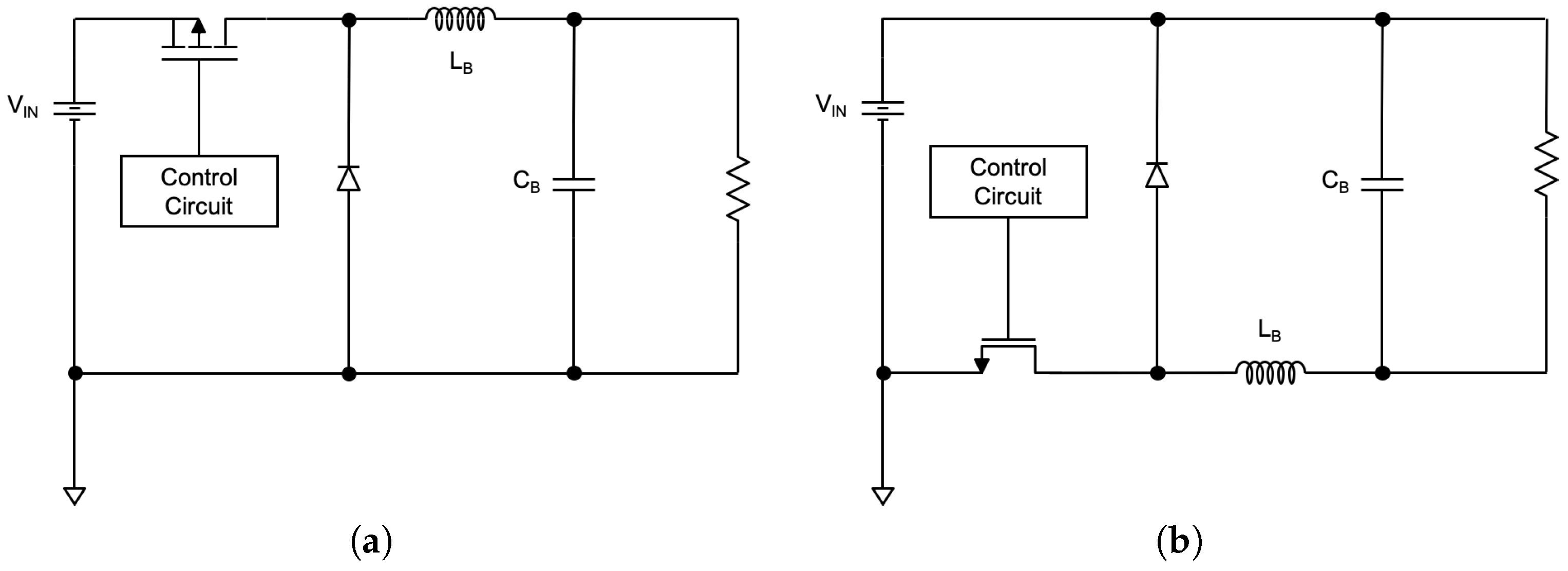
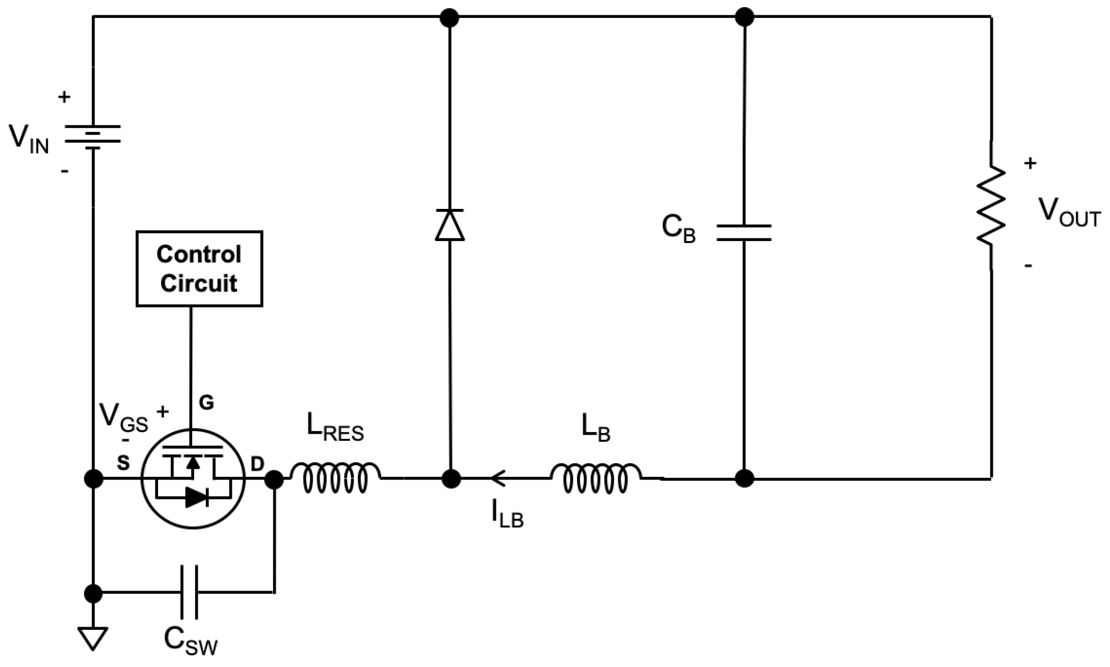
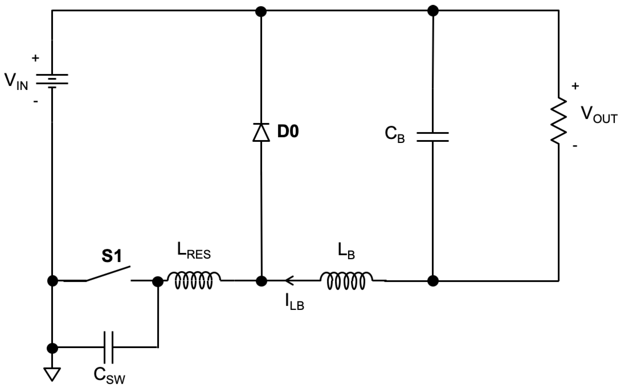
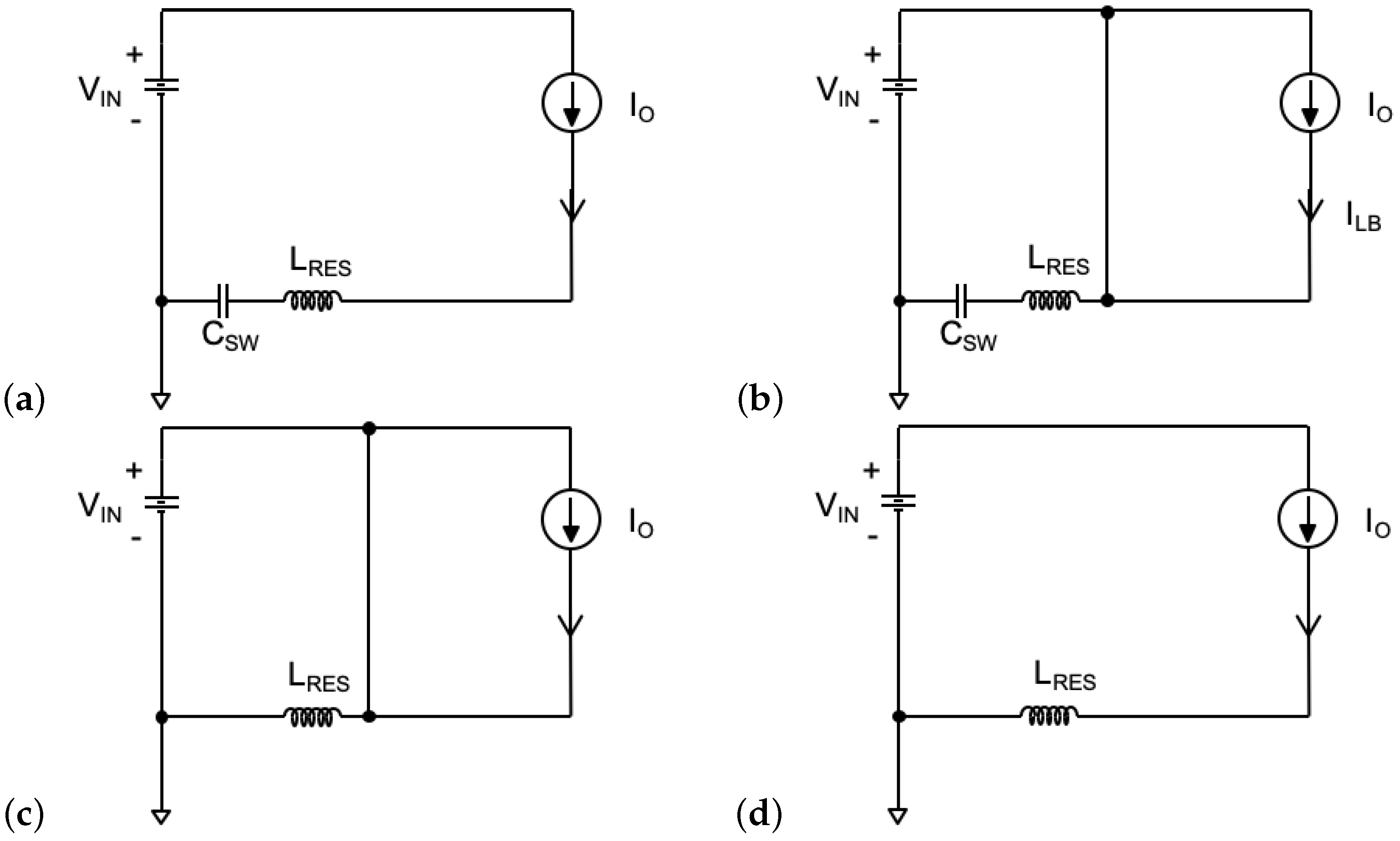
2.1. Quasi Resonant Floating Buck Converter Design

The load of a conventional buck converter design is ground referenced with inductor L B placed in series with the p-channel switch and the load. However, the difficulty in using a p-channel switch is that it requires a gate voltage beyond the input supply to turn on. This necessity demands an additional supply voltage solely for the high side gate drive. As a result, using an n-channel switch is more desirable as it is able to obtain a high efficiency in buck regulator application. This is because of the lower on-resistance of n-channel switches reducing switching losses. Compared to a conventional buck converter design, the terminals of the load of a floating buck converter design is floating, not referenced to ground. The comparison between conventional buck and the floating buck converter design is shown in Figure 2.
The floating buck configuration shown in Figure 2b is desired as n-channel FET is used as the power switch. GaN transistors are presently more commercially available as enhancement mode n-channel FETs. GaN is a wide-bandgap semiconductor developed in recent years to enable power FETs with superior performances over silicon-based FETs [12,13].
In order to enable high-frequency operation with high power efficiency, a quasi-resonant floating buck converter design was employed as shown in Figure 3. In this circuit, L R E S and C S W forms a resonant network such that the voltage at the drain terminal of the power switch comes close to zero just before the GaN FET turns on, therefore achieving ZVS [14]. The ZVS technique helps to minimize switching loss due to C S W and allows the buck converter to operate at high frequencies.
Assuming that L B is much bigger than L R E S and treating output filters L B , C B and R l o a d as the current source I o , four modes of operation for the quasi-resonant floating buck circuit can be derived. The circuit diagram of a floating buck ZVS quasi-resonant converter (QRC) is shown in Figure 4. The equivalent floating buck ZVS QRC circuits for the four modes of operation are shown in Figure 5.
In Mode 1, described by Figure 5a, the capacitor charges. Switch (S1) turns off at time T0, and the diode (D0) does not conduct. By conducting KCL and KVL, the two equations in Equation (1) are obtained. The boundary condition is described in Equation (2) and the duration of Mode 1 can be calculated with Equation (3).
C S W d V C S W d t = I o V C S W = I o ( t t o ) C S W
When V C S W increases to V I N , the voltage across the diode becomes positive and diode starts conducting as it is in forward bias.
Boundary Condition:
V C S W = V I N
Duration of this state:
t 01 = C S W V I N I o
In Mode 2, described by Figure 5b, S1 remains off whereas D0 conducts. Using KCL and KVL, the equations in Equation (4) are obtained.
C S W d V C S W d t = i L B L R E S d i L B d t = V I N V C S W
Solving the second-order differential equations described in Equation (4), we can get the time domain solutions shown in Equation (5).
i L B = I o cos ( ω o ( t t 1 ) ) V C S W = V I N + Z I o sin ( ω o ( t t 1 ) )
where
ω o = 1 L R E S C S W Z = L R E S C S W
It is noted that resonance stops when S1 turns on. As a result, the duration of Mode 2 can be calculated using Equation (6). The boundary condition is described by Equation (7).
t 12 = α ω o
where
α = sin 1 ( Φ ) = sin 1 ( V I N Z I o )
V C S W = 0
At t 2 ,
i L B ( t 2 ) = I o cos α
In Mode 3, described by Figure 5c, S1 turns on whereas D0 continues to conduct. Using KCL and KVL, the equations in Equation (8) are obtained. Resonance stops and L R E S is charged by input voltage V I N .
L R E S d i L B d t = V I N
Solving Equation (8) in time domain, the solution in Equation (9) is obtained.
i L B = I o cos α + V I N ( t t 2 ) L R E S
The boundary condition is described in Equation (10) and the duration of Mode 1 can be calculated with Equation (11).
i L B = I o
t 23 = L R E S I o cos α V I N
In Mode 4, described by Figure 5d, S1 remains on whereas D0 stops conducting. This stage is also known as the free-wheeling stage. Output current flows through L r and S1. Mode 4 ends when the transistor turns off again at t 4 . It should be noted that t 4 is the same as t 0 in the next cycle. The duration of this stage can be calculated using Equation (12).
t 34 = t p e r i o d t 01 t 12 t 23
where
t p e r i o d = period of the switching cycle
The use of the LC resonant network helps to shape the voltage waveform of the GaN switching device into a quasi-sine wave. Zero voltage conduction is therefore created for the GaN switch to turn on and off without incurring switching losses. As a result, this further reduces turn-on losses associated with the parasitic junction capacitances.
The circuit parameters that are set before calculation are V I N , V O U T , I O , f S W and R L . In order to determine the values of the passive elements, the inverted buck converter is first calculated without consideration of the resonant network using well known design methods like in [15,16,17]. Then, the resonant elements are calculated using a simplified set of expressions shown in Equations (14) and (15) [18].
Normalised load resistance, R , and resonant frequency, f o could be obtained with Equation (13). From Equation (14), the value of Z can be obtained. The value of f o could be substituted into Equation (15) for a value of D. Then, the value of L R E S and C S W could be determined Equation (13).
R = M = V O U T V I N = 1 3 π + 3 4 π ( f S W f o ) = 1 3 π + 3 4 π v
R = R L Z = R L ω o L R E S = ω o C S W R L = v R L ω s L R E S = ω s C S W R L v
D = 1 3 π + 2 4 π ( f S W f o ) = 1 3 π + 2 4 π v
The circuit parameters used in the design are listed in Table 1. The values of resonant inductor and resonant capacitor are calculated from the discussed design criteria.

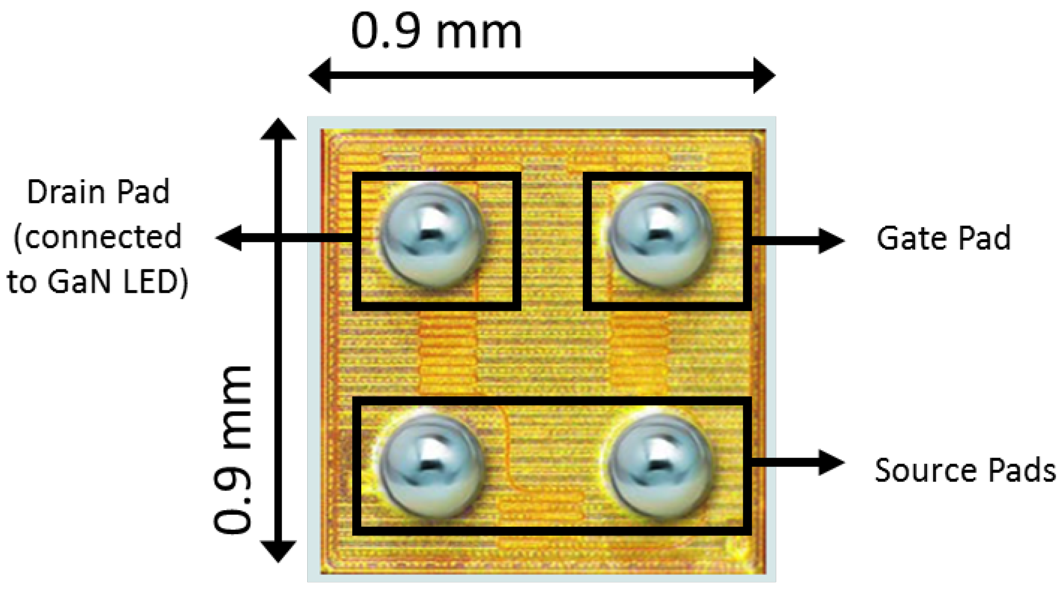
2.2. Assembly of GaN FETs

The power switch used in the LED driver schematic described in Figure 3 is EPC2036 GaN FET [19]. EPC2036 is available commercially in passivated die form as shown in Figure 6. The bonding pad terminals were designed with the top metal layer of the IC to match to the 3 terminals of the GaN FET. This is to enable the flip-chip (FC) bonding of the EPC2036 GaN FET die atop the BCD circuit.

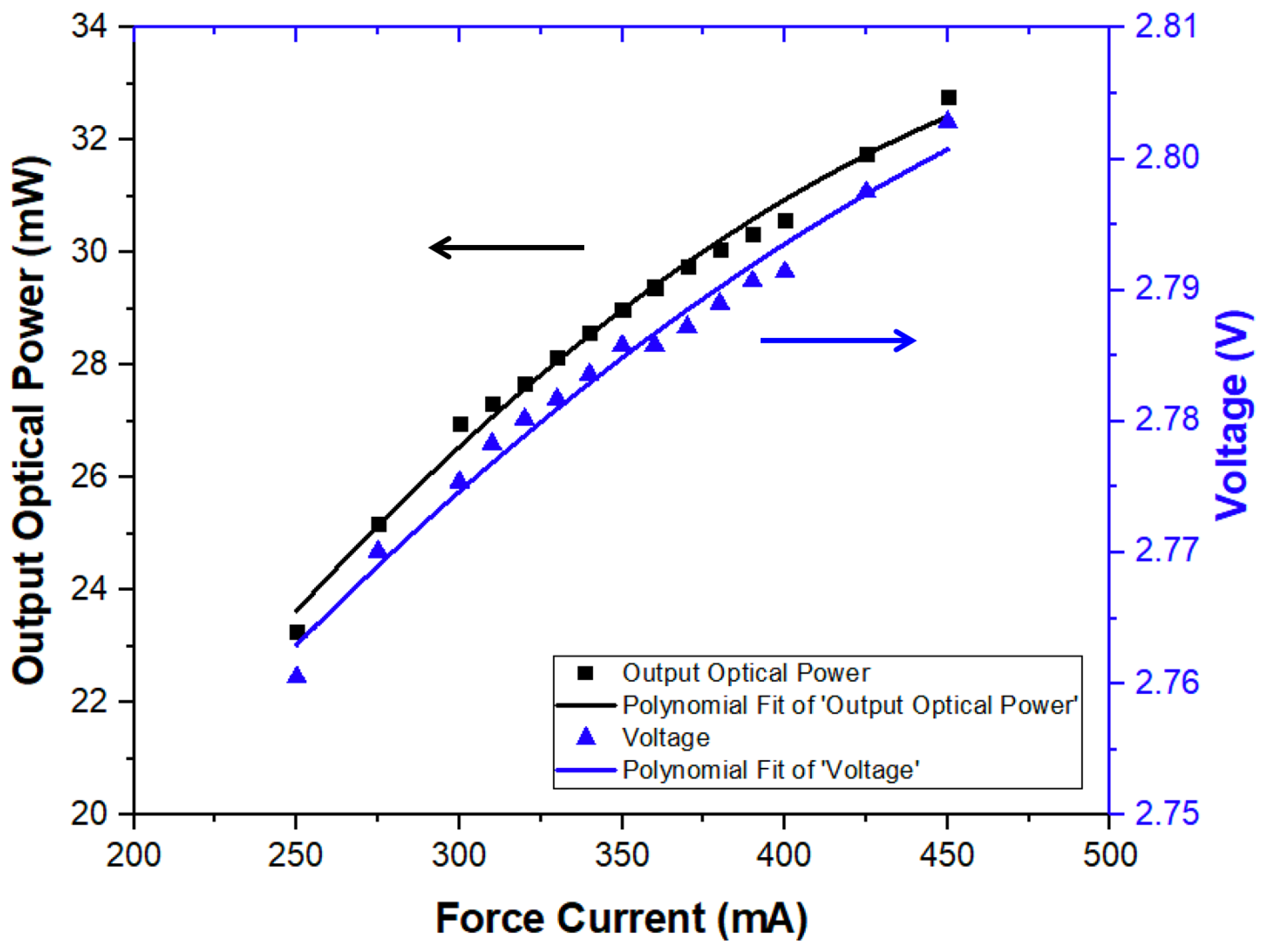
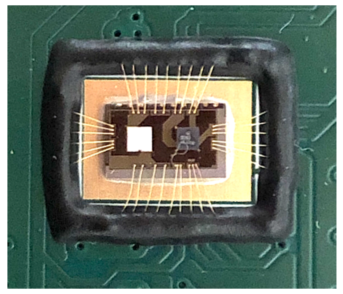
2.3. Fabrication and Assembly of Custom GaN LED

A customised GaN high-power FC LED (1 mm × 1 mm size) was designed such that its two terminals (the cathode and anode terminals) are on top. The LEDs were fabricated on 2-inch sapphire substrates with the top metal pads having a thick Au finish such that it is suited for solder bumping to the BCD circuits. It is noted that the sapphire substrate is transparent in order to allow for light emission after the FC bonding process. The measured graph of average output optical power versus forward bias current versus average forward bias voltage (P-I-V) of 7 LED devices is shown in Figure 7.

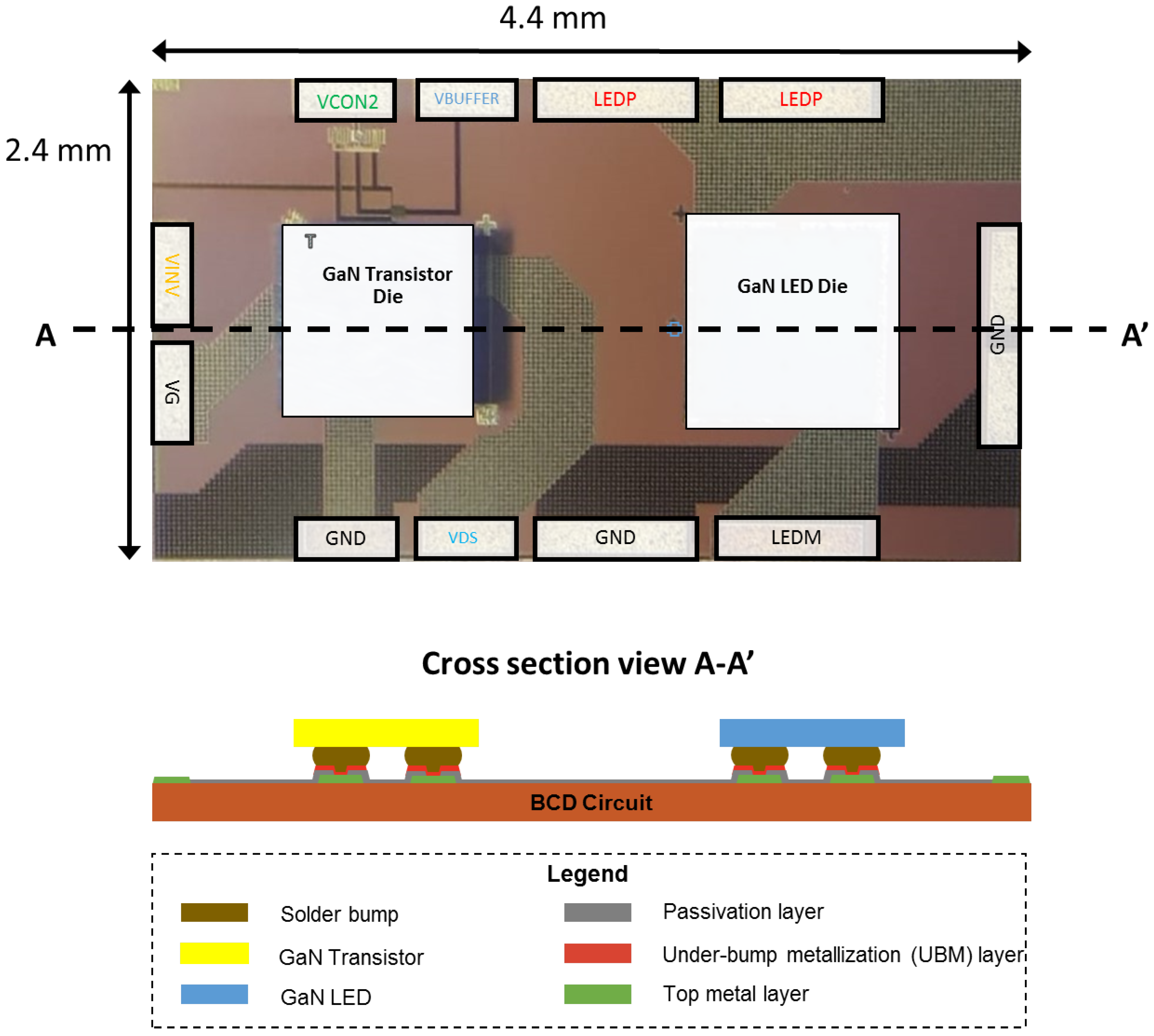
2.4. Fabrication of LED Driver IC

The driver IC was fabricated with GLOBALFOUNDRIES 0.18- μ m BCDlite TM technology. Following wafer fabrication, an under-bump metallization (UBM) layer is formed atop the top metallization layer of the IC chip. This allows for on-chip wafer level integration as shown in Figure 8. The UBM layer is required to provide good adhesion to the wafer passivation, serve as a low resistance and ohmic contact to the final metal on the wafer, as well as a robust solder diffusion barrier layer which is solder wettable [20,21].
The heterogeneous integration process is a 3-step process. First, solder is applied to the terminals of the GaN LED. It is noted that the commercially available packaged form of the EPC2036 comes with solder bumps; hence, it is not required to apply solder to its terminals. Second, both GaN elements (GaN FET and GaN LED) are FC bonded on top of the BCD circuit. The last step is reflow soldering. Wafer dicing takes place after both GaN devices are bonded on the wafer level. Figure 8 shows the layout of the bonding pad that is designed for FC bonding both GaN devices atop the BCD LED driver IC.

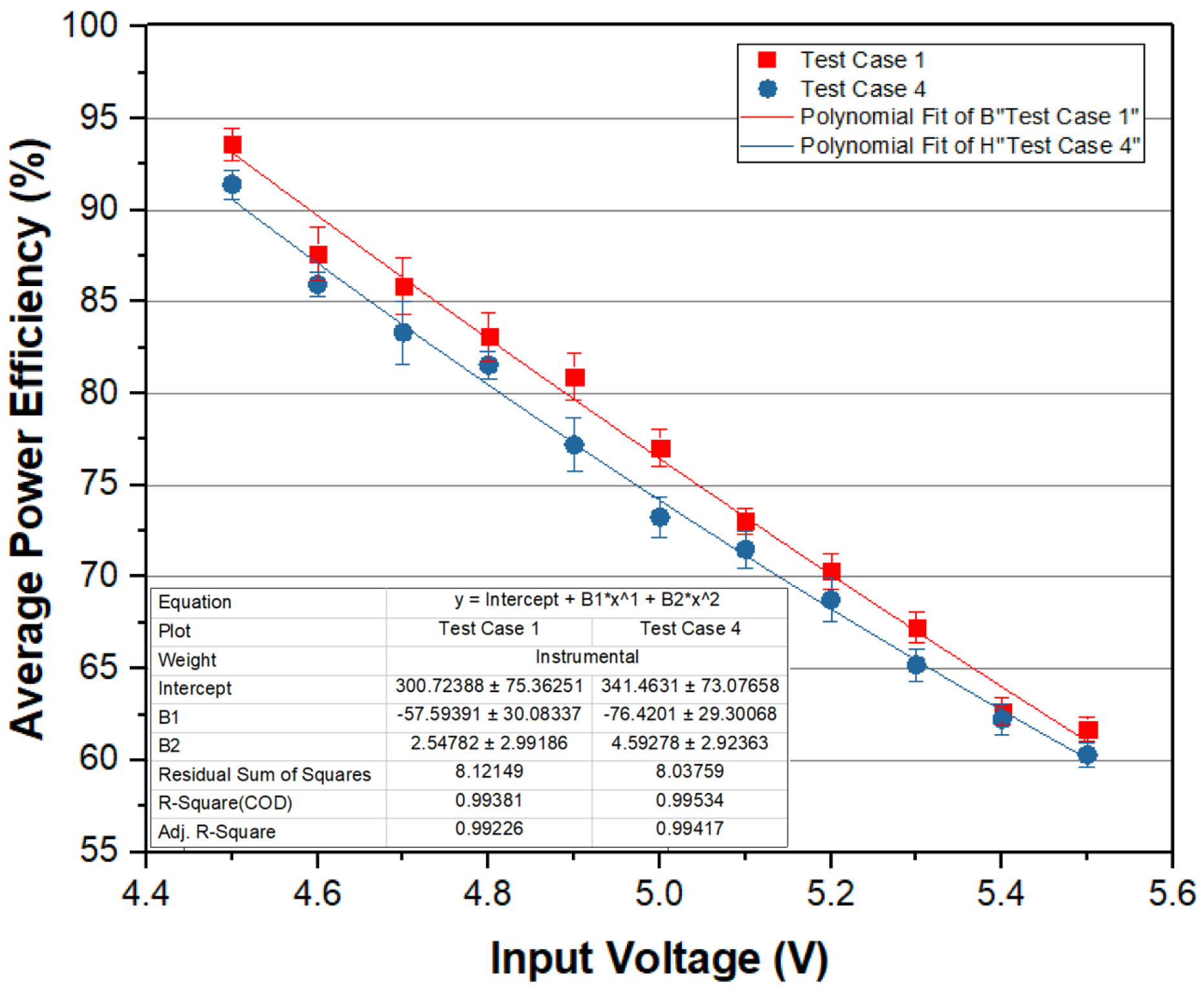
3. Measured Results and Discussions
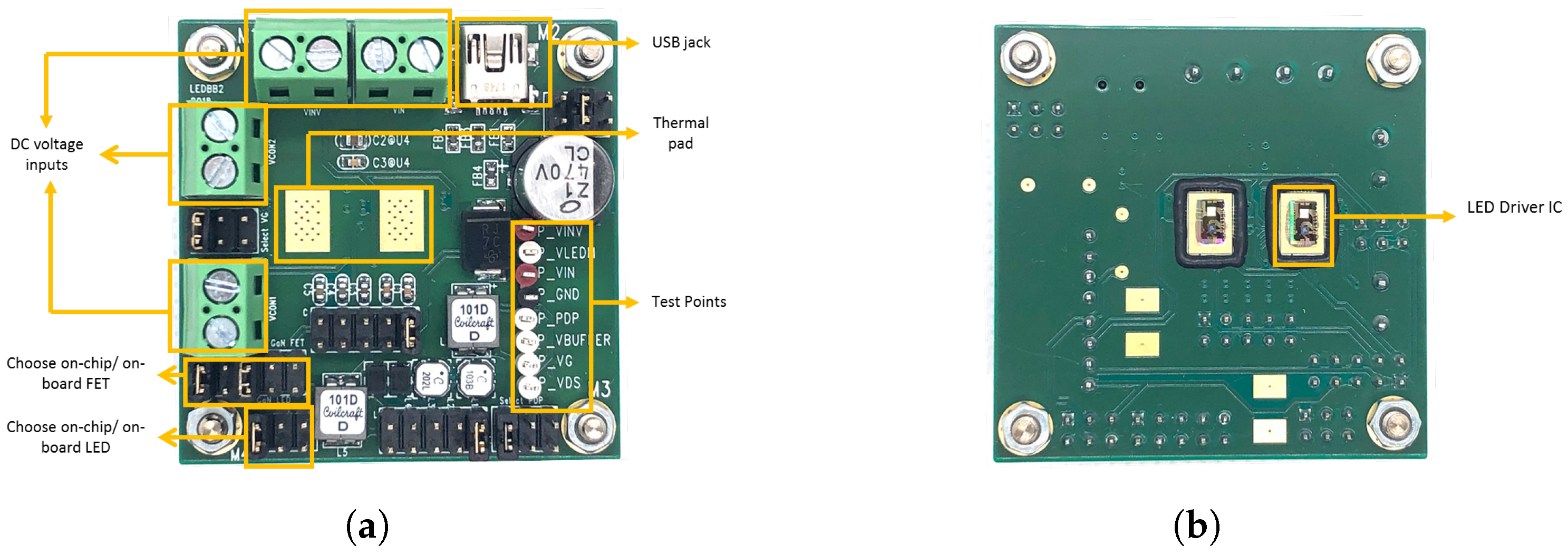
This section examines the obtained experimental results from the LED driver IC operation. A printed circuit board (PCB) as shown in Figure 9 is designed to validate and evaluate the performance of the proposed design with respect to the conventional fully on-board integration of power devices with LED driver IC.

3.1. PCB Design

As shown in Figure 10, The LED driver IC is wire-bonded to the PCB after the FC bonding process. The PCB evaluation board has a compact size of 50.9 × 51 mm 2 .

3.2. Functionality

The comparison of average power efficiency for fully on-chip and fully on-board integration of LED and FET device is shown in Figure 11. A total of 10 PCB boards for each test case were tested and evaluated to plot the graph of average power efficiency against input voltage. The red and blue error bars indicate the standard error of the power efficiency values obtained at each input voltage for Test Case 1 and Test Case 2 respectively. Test Case 1 and Test 2 are illustrated in Figure 1.
It can be observed that the trend line describing Test Case 1, which is the fully on-chip integrated LED driver, has a consistently higher average power efficiency value compared to Test Case 2, which is the conventional fully on-board LED driver design. For Test Case 1, as both the GaN LED and GaN FET are integrated directly on top of the LED driver IC, there is no need for additional connections to connect the IC to the LED die and FET die on the PCB. This reduces the parasitic resistance inherent in conventional LED driver design, resulting in an improved power efficiency value. It is noted that the maximal percentage improvement in efficiency of the on-chip solution compared with the on-board solution is 18%. The valid input voltage is from 4.5 V to 5.5 V and the needed output voltage range is 2.25 V to 2.75 V. At 4.5 V input voltage, the average power efficiency value obtained for the on-chip solution is 92.5%. In addition, the proposed on-chip design is 29% smaller in size as compared to the conventional on-board design.

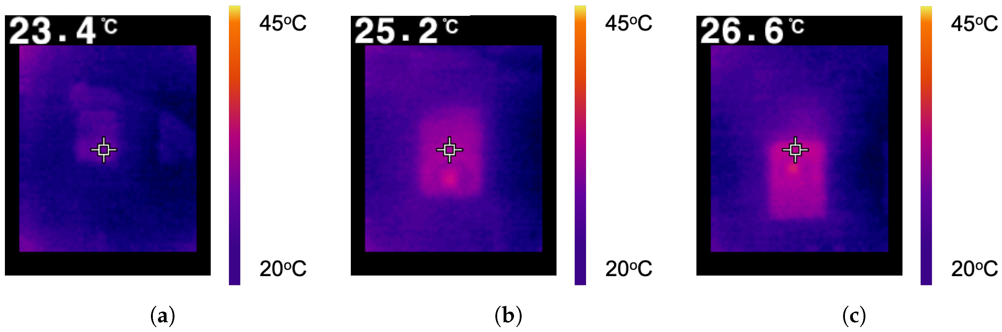
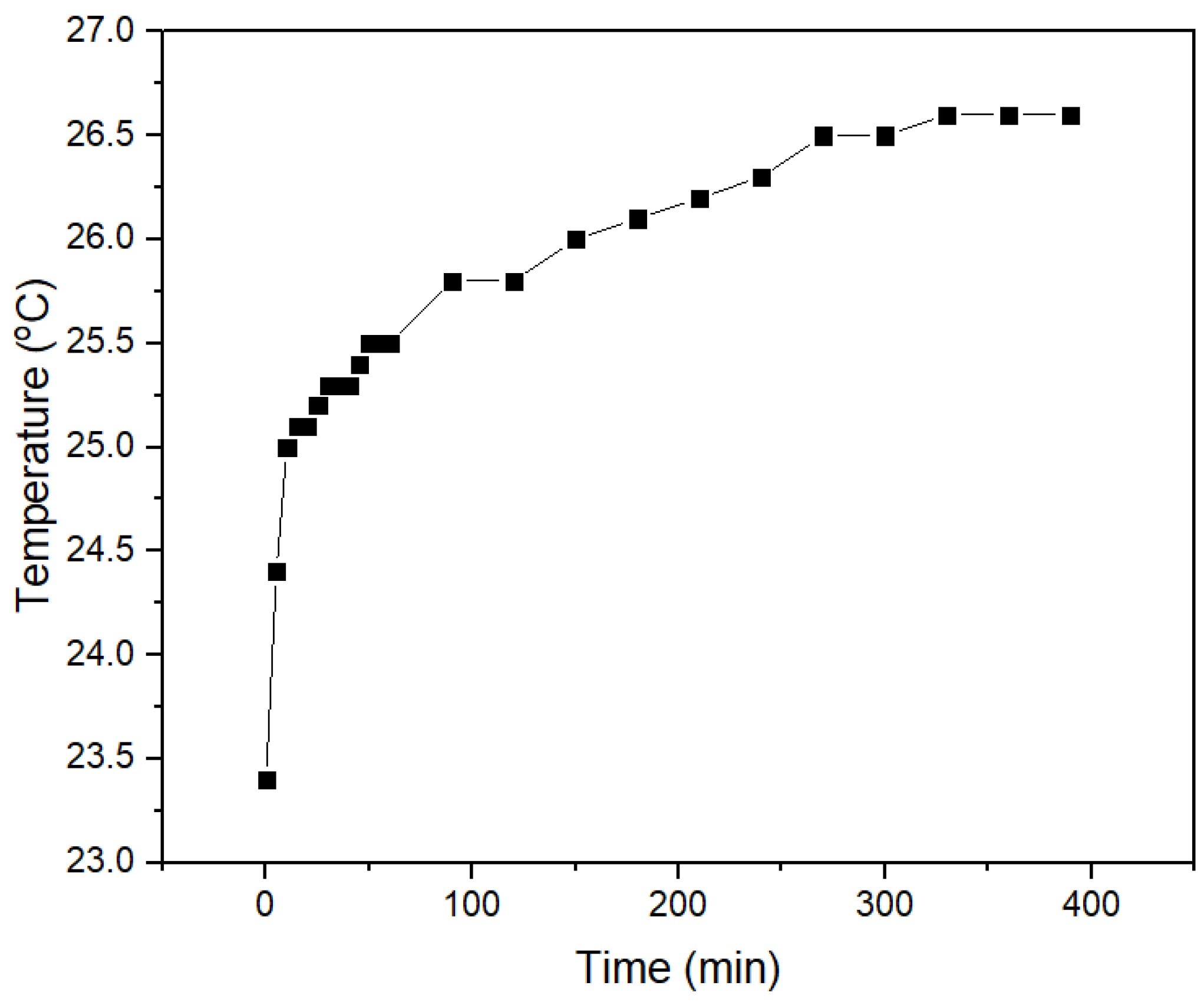
3.3. Thermal Testing

The results of thermal testing for the dedicated thermal pad on PCB designed for thermal dissipation is discussed in this section. In order to verify if Test Case 2 (on-chip solution) would pose thermal dissipation concern, thermal testing using an infrared (IR) thermometer (FLIR TG165 [22]) was carried out before and during operation of the designed LED driver. Figure 12 presents the IR image of the thermal pad taken at 0, 30 and 180 minute intervals during circuit operation. Figure 13 illustrates the graph of the surface temperature of the dedicated thermal pad on the PCB (°C) against time (min).
The maximal surface temperature of any device designed for the human touch is 70 °C based on the IEC standard for consumer electronics devices (IEC’s 60950-1 (2005) [23]). As shown in Figure 13, the maximal surface temperature over 6 h of continuous operation for the proposed on-chip solution is 26.6 °C, hence it can be concluded that there is no thermal dissipation concern using the on-chip bonding solution.

4. Conclusions

A fully on-chip integrated LED driver has been designed, verified and implemented using heterogeneous integration of GaN power devices (both GaN LED and GaN transistor) directly on top of BCD circuits. The performance of the proposed design has been compared with the conventional fully on-board integration of power devices with the LED driver IC. Experimental results confirm that the fully on-chip integrated LED driver achieved a consistently higher efficiency value as compared with the fully on-board design within the input voltage range of 4.5–5.5 V. This work is enabled with GLOBALFOUNDRIES GaN2BCD TM technology. This novel technology has achieved an average power efficiency of 92.5% with a reduced size of 29% for LED driver design. Future work involves improving the integration level of the LED driver design by integrating on-chip magnetic components, improving the driving circuitry with considerations on control algorithm and further reduction of parasitic inductances with PCB design.

Author Contributions

M.Y.S. designed, analysed, built and carried out experiments on the integrated LED circuit; S.L.S., L.P. and K.S.Y. contributed to the concept of heterogeneous integration and its specification. All authors have read and agreed to the published version of the manuscript.

Acknowledgments

The authors acknowledge the funding from the Economic Development Board (EDB) of Singapore for the research grant to support this research project. The customized LEDs described in this paper were fabricated by Luminous! Semiconductor Lighting and Display Center of Excellence, EEE, NTU, Singapore. The authors would like to thank the technical support from Mr. Wong Thin Sek.

Conflicts of Interest

The authors declare no conflict of interest.

Abbreviations

The following abbreviations are used in this manuscript:
BCDBipolar CMOS DMOS
CMOSComplementary-Metal-Oxide-Semiconductor
DMOSDouble-Diffused Metal-Oxide Semiconductor.
FETField Effect Transistor
FCFlip-Chip
EDBEconomic Development Board
ICIntegrated Circuits
IRInfrared
KCLKirchhoff’s Current Law
KVLKirchhoff’s Voltage Law
LEDLight-Emitting Diode
MCPCBMetal-Core Printed Circuit Board
MDPIMultidisciplinary Digital Publishing Institute
NTUNanyang Technological University
PCBPrinted Circuit Board
QRCQuasi Resonant Converter
SUTDSingapore University of Technology and Design
UBMUnder-Bump Metallization
ZVSZero Voltage Switching

References

  1. Craford, M.G. An overview of visible light emitting diode (LED) development and the potential for AlInGaP devices. IEEE Trans. Electron Devices 1993, 40, 2098. [Google Scholar] [CrossRef]
  2. Qu, X.; Wang, H.; Zhan, X.; Blaabjerg, F.; Chung, H.S. A Lifetime Prediction Method for LEDs Considering Real Mission Profiles. IEEE Trans. Power Electron. 2017, 32, 8718–8727. [Google Scholar] [CrossRef] [Green Version]
  3. Soh, M.Y.; Ng, W.X.; Zou, Q.; Lee, D.; Teo, T.H.; Yeo, K.S. Real-Time Audio Transmission Using Visible Light Communication. In Proceedings of the 2018 IEEE Region 10 Conference, Jeju, Korea, 28–31 October 2018; pp. 2223–2226. [Google Scholar] [CrossRef]
  4. Li, L.; Gao, Y.; Jiang, H.; Mok, P.K.; Lau, K.M. An Auto-Zero-Voltage-Switching Quasi-Resonant LED Driver With GaN FETs and Fully Integrated LED Shunt Protectors. IEEE J. Solid-State Circuits 2018, 53, 913–923. [Google Scholar] [CrossRef]
  5. Bandyopadhyay, S.; Neidorff, B.; Freeman, D.; Chandrakasan, A.P. 90.6% Efficient 11 MHz 22 W LED driver Using GaN FETs And Burst-Mode Controller With 0.96 Power Factor. In Proceedings of the 2013 IEEE International Solid-State Circuits Conference Digest of Technical Papers, San Francisco, CA, USA, 17–21 February 2013; pp. 368–369. [Google Scholar] [CrossRef] [Green Version]
  6. Caring Circuit. PCB Prototyping Fabrication Price Table. Available online: http://www.caringcircuit.com/fab-pcb-price-qt-1.html (accessed on 12 December 2019).
  7. Meng, F.; Disney, D.; Liu, B.; Volkan, B.; Zhou, A.; Liang, Z.; Yi, X.; Selvaraj, L.; Peng, L.; Ma, K.; et al. Heterogeneous Integration of GaN and BCD Technologies and Its Applications to High Conversion-ratio DC-DC Boost Converter IC. IEEE Trans. Power Electron. 2019, 34, 1993–1996. [Google Scholar] [CrossRef]
  8. Soh, M.Y.; Teo, T.H.; Selvaraj, S.L.; Peng, L.; Disney, D.; Yeo, K.S. Design of fully integrated low-power low-voltage LED lighting with heterogeneous integration of GaN and BCD Technologies. MDPI Electron. 2019, 8, 351. [Google Scholar] [CrossRef] [Green Version]
  9. Soh, M.Y.; Ng, W.X.; Teo, T.H.; Selvaraj, S.L.; Peng, L.; Disney, D.; Zou, Q.; Yeo, K.S. Design and Characterization of Micro-LED Matrix Display With Heterogeneous Integration of GaN and BCD Technologies. IEEE Trans. Electron Devices 2019, 66, 4221–4227. [Google Scholar] [CrossRef]
  10. Liu, M.; Hsu, S.S.H. A Miniature 300-MHz Resonant DC–DC Converter With GaN and CMOS Integrated in IPD Technology. IEEE Trans. Power Electron. 2018, 33, 9656–9668. [Google Scholar] [CrossRef]
  11. Selvaraj, S.L.; Peng, L.; Qiong, Z.; Seng, Y.K.; Disney, D. Heterogeneous Integration of GaN LED on CMOS Driver Circuit for Mobile Phone Applications. In Proceedings of the 2018 IEEE 2nd Electron Devices Technology and Manufacturing Conference (EDTM), Kobe, Japan, 13–16 March 2018; pp. 71–73. [Google Scholar] [CrossRef]
  12. Mojab, A.; Hemmat, Z.; Riazmontazer, H.; Rahnamaee, A. Introducing Optical Cascode GaN HEMT. IEEE Trans. Electron Devices 2017, 64, 796–804. [Google Scholar] [CrossRef]
  13. Hahn, H.; Funck, C.; Geipel, S.; Kalisch, H.; Vescan, A. The III-Nitride Double Heterostructure Revisited: Benefits for Threshold Voltage Engineering of MIS Devices. IEEE Trans. Electron Devices 2016, 63, 606–613. [Google Scholar] [CrossRef]
  14. Tabisz, W.A.; Lee, F.C. Zero-Voltage-Switching Multiresonant Technique-A Novel Approach To Improve Performance Of High-Frequency Quasi-Resonant Converters. IEEE Trans. Power Electron. 1989, 4, 450–458. [Google Scholar] [CrossRef]
  15. Rashid, M.H. Power Electronics Handbook: Devices, Circuits and Applications; Elsevier: Amsterdam, The Netherlands, 2010. [Google Scholar]
  16. Mack, R.A. Demystifying Switching Power Supplies; Elsevier: Amsterdam, The Netherlands, 2011. [Google Scholar]
  17. Mohan, N.; Undeland, T.M.; Robbins, W.P. Power Electronics: Converters, Applications, and Design; John Wiley & Sons: Hoboken, NJ, USA, 2003. [Google Scholar]
  18. Hinov, N.L.; Rangelov, N.R. Buck ZVS DC-DC Quasi-Resonant Converter: Design, Modeling, Simulation and Experimentation. Annu. J. Electron. 2015, 9, 232–237. [Google Scholar]
  19. Corporation, E.P.C. EPC2036—Enhancement Mode Power Transistor; PC Corporation: El Segundo, CA, USA, 2018. [Google Scholar]
  20. Jang, S.Y.; Wolf, J.; Ehrmann, O.; Gloor, H.; Schreiber, T.; Reichl, H.; Paik, K.W. CrCu based UBM (under bump metallization) study with electroplated Pb/63Sn solder bumps-interfacial reaction and bump shear strength. IEEE Trans. Compon. Packag. Technol. 2003, 26, 245–254. [Google Scholar] [CrossRef] [Green Version]
  21. Chan, K.; Zhong, Z.; Ong, K. Study of under bump metallisation barrier layer for lead-free solder. Solder. Surf. Mt. Technol. 2003, 15, 46–52. [Google Scholar] [CrossRef]
  22. FLIR. FLIR TG165 Imaging IR Thermometer; FLIR: Wilsonville, OR, USA, January 2017. [Google Scholar]
  23. International Electrotechnical Commission. Information Technology Equipment-Safety—Part 1: General Requirements [IEC 60950–1-Ed. 1]; International Electrotechnical Commission: Geneva, Switzerland, 2001. [Google Scholar]
Figure 1. Illustration of DoE based on on-chip or on-board integration of LED and FET device.
Electronics 09 00575 g001
Figure 2. Comparison of schematics for (a) conventional buck converter and (b) floating buck converter.
Electronics 09 00575 g002
Figure 3. Floating Buck Quasi Resonance Circuit.
Electronics 09 00575 g003
Figure 4. Floating Buck ZVS-QRC Circuit Diagram.
Electronics 09 00575 g004
Figure 5. Equivalent Floating Buck ZVS-QRC Circuit in (a) Mode 1 (duration of t 01 ), (b) Mode 2 (duration of t 12 ), (c) Mode 3 (duration of t 23 ), and (d) Mode 4 (duration of t 34 ).
Electronics 09 00575 g005
Figure 6. EPC2036 in passivated die form with solder bumps.
Electronics 09 00575 g006
Figure 7. Average P-I-V curve of 7 LED devices.
Electronics 09 00575 g007
Figure 8. Photograph indicating bond pad layouts for bonding of GaN elements atop LED driver IC with the cross-section sketch view depicting the G a N 2 B C D T M technology.
Electronics 09 00575 g008
Figure 9. (a) Front side and (b) back side of PCB.
Electronics 09 00575 g009
Figure 10. LED driver IC wire-bonded to the PCB following FC bonding process.
Electronics 09 00575 g010
Figure 11. Comparison of performance for fully on-chip or fully on-board integration of LED and FET device.
Electronics 09 00575 g011
Figure 12. IR image of thermal pad (a) before operation, (b) after 30 min operation, (c) after 6 h operation.
Electronics 09 00575 g012
Figure 13. Surface temperature of the dedicated thermal pad (°C) against time (min).
Electronics 09 00575 g013
Table 1. Circuit parameters.
Circuit ParameterValue
V I N 5 V
V O U T 2.5 V
L B 2 uH
C B 10 uF
L R E S 100 nH
C S W 90 pF
f S W , switching frequency11 MHz
f o , resonant frequency21.8 MHz

