


Abstract
In this paper, a new method of structural decomposition is proposed. The method focuses on FPGA-based Moore finite state machines (FSMs). The method makes it possible to improve both spatial and temporal characteristics of the FSM circuits. Each internal state is represented by two codes. One of them is a partial state code representing a state as an element of some class of compatibility. The second code is represented by a concatenation of two codes: a code of output collection and a code of identifier. The method can be applied if FSM circuits are implemented using look-up table (LUT) elements of field-programmable gate arrays. The resulting FSM circuit includes three logic blocks. The first block generates partial Boolean functions representing partial output collections and identifiers. These functions depend on partial state codes. The partial codes are assigned in a way minimizing the number of arguments in partial functions. This allows generating all partial functions by single-LUT circuits. The second block generates codes of output collections and identifiers. The third block transforms them into FSM outputs and partial state codes. The paper includes an example of FSM synthesis by applying the proposed method. The experiments are conducted using standard benchmark FSMs. The experiments show that the proposed approach can be used for complex FSMs where the total number of FSM inputs and state variables are at least twice the number of inputs of the base LUT. The results of experiments show that the proposed method allows improving both the spatial and temporal characteristics for complex FSMs compared with their counterparts based on methods used by the Vivado tool.
1. Introduction
Nowadays, a model of a finite state machine (FSM) is a powerful tool used for representing various sequential blocks [1,2,3]. For example, this model is used for representing the control units of computers [4,5,6,7,8], hardware–software interfaces and communication protocols of embedded systems [9] and in many other cases [10,11,12,13,14,15,16]. It could even be used for the synthesis of both a control unit and a data path, creating a single operational block [17,18,19]. This wide range of applications is a source of developing new methods for synthesizing and optimizing characteristics of FSMs. The optimization methods depend significantly on the specifics of the logic elements used for implementing the FSM circuit. Also, they depend on peculiarities of an FSM model used [3]. In this paper, we propose a method for reducing the chip area occupied by circuits of Moore FSMs.
The majority of papers and monographs deal with Mealy FSMs. The reason for this situation is that Mealy FSMs can have significantly fewer states than equivalent Moore FSMs [20]. This leads to the conclusion that circuits of Mealy FSMS will require fewer resources than it is for equivalent Moore FSMs. But the outputs of Moore FSMs depend only on internal states. As a result, a part of the logic circuit that generates outputs is simpler for Moore FSMs than for equivalent Mealy FSMs. Moreover, Mealy FSMs are unstable because their outputs depend directly on their inputs. This dependence leads to the following phenomena: rattling of the inputs results in glitches in the outputs. In turn, these glitches could result in improper functioning of the system of which an FSM is a part. To stabilize the outputs, an addition register is introduced in the FSM circuit. This register consumes some chip resources and increases the cycle time. There are no output glitches in Moore FSMs. As a result, the circuits of Moore FSMs require fewer flip-flops and can be faster than those of equivalent Mealy FSMs. These positive features of Moore FSMs explain our choice of this model as a research subject.
We discuss a case when FSM circuits are implemented using the internal resources of field-programmable gate arrays (FPGAs) [21,22,23]. Our choice is justified by the fact that, starting from 1984, these chips have been widely applied for implementing diversified digital systems [24]. The architectures of FPGA chips are constantly being improved [25,26]. The leading experts are sure that FPGAs will play an important role in the development of various hardware tools for artificial intelligence [27]. This means that FPGAs will continue to be used in the foreseeable future [28]. In this paper, we discuss a case in which the logic circuits of Moore finite-state machines are implemented using fine-grain configurable logic blocks (CLBs) based on look-up table (LUT) elements.
In the paper, we discuss SRAM-based single-output LUTs having inputs [21,23]. Such LUTs are used in FPGA chips produced by AMD Xilinx [29]. This company occupies a leading position in the FPGA market. Each SRAM cell keeps one bit of information. Using LUT inputs allows transferring the content of a particular cell to the LUT output. Due to it, a LUT generates a Boolean function dependent on up to arguments [30,31]. To be a flexible logic element, each LUT has very small value of (around six) [21,23]. This is a specific required using the functional decomposition (FD) of functions to be generated. The FD-based methods allow representing initial systems of Boolean functions (SBFs) as compositions of partial functions [31,32]. This leads to obtaining multi-level FSM circuits [3].
Very often, the criterion of optimality for an FSM circuit is a minimum chip area occupied [33,34]. As a rule, optimizing the required chip area diminishes the value of power consumed by an FSM circuit [35,36,37]. In the best case, optimizing chip area does not significantly increase the time of the operation cycle. In this paper, we propose a method that allows reducing the required chip area without a decrease in the maximum operating frequency of the resulting Moore FSM circuit.
As it is known [37], the spatial characteristics of a LUT-based FSM circuit are determined mostly by the number of LUTs consumed (LUT count) and the system of inter-CLB interconnections. Thus, to reduce the chip area occupied by an FSM circuit, it is necessary to diminish the number of LUTs required. Also, it is necessary to optimize the system of interconnections. This is connected with the following issues. Firstly, the delay associated with interconnections now dominates the delay associated with logic [30,38]. Also, the interconnection system consumes up to 70% of power [39]. So, optimizing interconnections reduces both circuit delay and power consumption.
As shown in [24], the value SL = 6 provides the optimal balance among LUT characteristics such as occupied chip area, delay, and power consumption. This means that we cannot expect that the number of LUT inputs will be increased in the foreseeable future. But we witness the constant growth of the complexity of FPGA-based projects [14,40]. So, it is necessary to develop efficient design methods to overcome this specific feature of LUTs.
In this paper, we propose a new design method allowing to improve the LUT counts in the circuits of Moore FSMs. The proposed method is based on representing state codes as concatenations of codes of output collections (OC) and identifiers. The main contributions of our current work are the following:
- 1.
- A new design method allowing for improving two main characteristics of FPGA-based circuits of Moore FSMs (LUT count and performance).
- 2.
- Finding the conditions for applying the proposed method.
- 3.
- Conducting the experiments showing the positive and negative sides of the proposed method.
The main idea of the proposed method is to represent state variables as functions of variables encoding OCs and identifiers. We use this approach for Moore FSMs with twofold state codes. The proposed method belongs to methods of structural decomposition (SD). Using this method allows designing three-level Moore FSM circuits having fewer LUTs than their counterparts based on functional decomposition.
The remained part of the paper includes five sections and a brief conclusion. In the paper, we show: 1) the background of Moore FSMs and FPGAs (Section 2); 2) the state-of-the-art in FSM-based design (Section 3); 3) the proposed design method (Section 4); 4) an example of FSM design using the proposed method (Section 5) and 5) the experimental results (Section 6) and their discussion (Section 7).
To improve the readability of the paper, we create Table 1. The table includes most of the sets, variables, and blocks, and identifies their meanings.
Table 1.
Summarized notation table.
2. Background Information
As a rule, modern FPGAs include diversified CLBs (for example, LUTs, digital signal processors, embedded memory blocks) and a matrix of programmable interconnections [21,22,23,29,41]. In this article, we consider design based on CLBs consisting of LUTs and programmable flip-flops. There is a wired connection between the LUT output and informational input of a flip-flop. In the case of FSM-based projects, these flip-flops are used for organizing either registers or counters keeping state codes [42].
The main peculiarity of a LUT is a very limited value of . Nowadays, the value of does not exceed 6 [21,22,23]. If a Boolean function to be generated depends on at least 1 + variables, then the corresponding circuit should be implemented using FD-based methods [31]. As a result, such FSM circuit is multi-level. Moreover, the CLBs are connected using the irregular interconnect system. As shown in [3], irregular interconnect systems are slower and require more power than their SD-based counterparts.
The mathematical model of Moore FSM is a six-tuple [42] including the following components: ... is a set of internal states, ... is a set of external inputs, ... is a set of FSM outputs, is a transition function, is an output function, and is an initial state. So, an FSM has M states, L inputs and N outputs. In the starting point of operation, a Moore FSM should be set into the state . Various tools are used for representing this six-tuple. On of the most visual types of representation is a state transition table (STTs) [1]. Thanks to this clarity, we use these tables in our paper.
The STT can be viewed as a list of transitions existed into a state transition graph (STG). If an STG has M nodes, then the corresponding STT describes transitions from M states . If transitions are shown for a state , this state is called a current state. They are written in the column of STT. For STG of a Moore FSM, the CO is written, where .... In the STT, these COs are written into the column of current states. In STG, interstate transitions are represented by arcs directed from the current states to states of transitions. The states of transitions are placed into the column of STT. If there are H arcs in an STG, then there are H lines in the equivalent STT. In the STG, the input signal determined a particular transition is written above the corresponding arc. The signal is represented by a conjunction of inputs (or their compliments) determined a particular transition. In the STT, this signal is written into a column . So, an STT consists of columns , , , h.
To implement an FSM circuit, it is necessary to create two SBFs [42]. To do it, it is necessary to replace states by their binary codes. This is done during the step of state assignment [1,42]. During this step, each FSM state is represented by a binary code . These codes include R bits. Each bit corresponds to a state variable ... where T is a set of state variables. The minimum possible value of R is provided by the maximum binary state assignment when
The Equation (1) determines the maximum binary codes (MBCs). These codes are very popular; they are used in many academic CAD systems [43,44]. Also, this style is used by industrial CAD tools [45,46].
State codes are kept into a special state register (RG). As a rule, in FPGA-based design, the state register is constructed using synchronous D flip-flops [3]. These flip-flops have the shared inputs of synchronization (Clock) and reset (Start). To change the content of RG, special input memory functions (IMFs) are used. These functions form a set of IMFs ....
To design an FSM circuit, it is necessary to represent: (1) FSM outputs as functions depended on state variables and (2) IMFs as functions depended on both state variables and FSM inputs. The following SBFs represent a circuit of Moore FSM:
These SBFs are derived from a direct structure table (DST). The DST includes the columns of STT (, , , h) and the columns , , . Obviously, the column includes the codes of current states, while the column contains the codes of the states of transitions. The column includes IMFs determining the change of RG’s content from to .
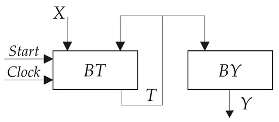
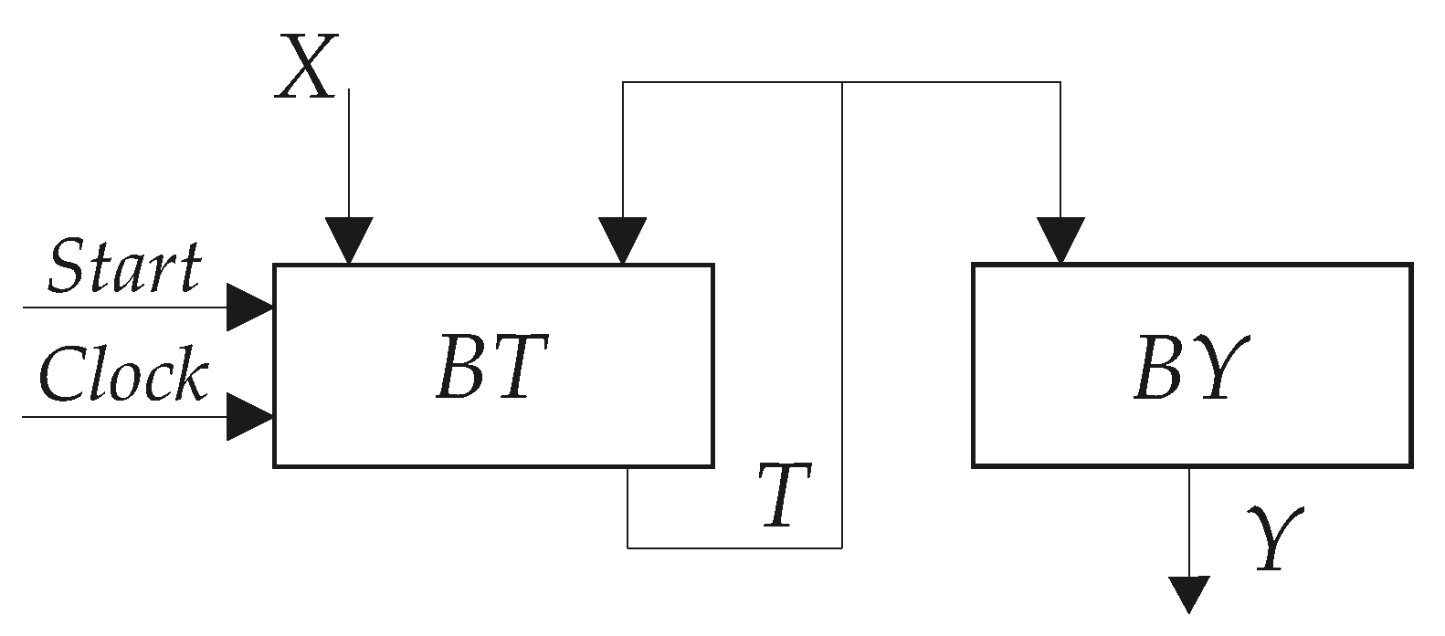
To generate functions , it is necessary to use at least R LUTs. These LUTs are combined into a block BT. To generate outputs , it is necessary to use at least N LUTs. These two blocks of LUTs represent a LUT-based logic circuit of Moore FSM (Figure 1) [36,47].
Figure 1.
Structural diagram of LUT-based Moore FSM .
In FSM , the block implements SBF (2), the block generates functions from SBF (3). The block includes a hidden state register distributed among its LUTs. This register transforms IMFs into state variables. To control the operation of RG, the signals of clearing (Start) and synchronization (Clock) enter the block .
One of the specifics of Moore FSM follows from (3): FSM outputs do not depend on FSM inputs. Due to it, the outputs could be generated by embedded memory blocks [3]. But it this paper, only LUT-based FSMs are discussed. However, the specific mentioned above makes easier the optimization process for the block . We discuss some possibilities of optimization in the next sections.
3. State-of-the-Art
The transition from an STT (or other form of FSM representation) to LUT-based electrical circuit is executed during the step of technology mapping [8,48]. This process is connected with necessity of solution of some optimization problems. The classical problems are: (1) minimizing the chip area occupied; (2) maximizing the operating frequency; (3) minimizing the power consumption; (4) increasing the testability of FSM circuit [3,49]. The fast development of intelligent tools [25,27] has raised the problem of increased security for FPGA-based projects [26]. In this paper, a method is proposed aimed at solving the first problem. To reduce the required chip area, it is necessary to minimize the value of LUT count (the number of LUTs required) and reduce the total length of inter-CLB interconnections [3].
We use the symbol for the number of literals [1] in sum-of-products (SOPs) of Boolean functions . The relation between values of and determines the number of levels in LUT-based FSM circuit [3]. Consider the following condition:
If (4) holds, then an FSM circuit is single-level.Such a circuit consists of LUTs. Also, this is the fastest from all possible circuits for a given FSM. But it is necessary at least two levels of LUTs for generating functions for which the condition (4) is not met. Obviously, the LUT count should be minimized (if it is possible). To optimize the interconnection system, it is necessary to produce a circuit where the same inputs and state variables appear only on a single logic level. Otherwise, the circuit has a system of «spaghetti-type» interconnections [3]. As shown in [50], the circuits with regular system of interconnections consume less power and are faster than their counterparts with the spaghetti-type interconnections.
Let us briefly analyze the approaches which allow optimizing FPGA chip area occupied by a Moore FSM circuit. There are three basic methods aimed at solution of this problem: (1) the functional decomposition of SBFs (2) and (3) [4,31,51,52]; (2) the optimal state assignment [1,3,53]; (3) the structural decomposition of FSM circuits [3,50,54].
The FD-based methods use the following approach. If the condition (4) is not met, then a Boolean function is represented as a composition of partial Boolean functions. Each partial function should include no more than literals. This approach is based on the Shannon decomposition [52] and allows representing any Boolean function as an expression using disjunction, conjunction and negation. The initial function should be decomposed into one of the variables. As a result, the function is represented as a combination of two other functions that depend on the remaining variables. The functional decomposition is a very powerful tool used in the process of FPGA-based technology mapping [52,55]. Applying FD leads to appearing new functions different from (2) and (3). Each of this functions requires a single LUT to be generated. If the condition (4) is violated, then the logic circuit of FSM includes LUTs, where NF1 is the number of new functions different from and . The FD-based program tools could be found in academic CAD tools [43,44], as well as in industrial CAD packages [56,57,58].
Obviously, FD-based circuits are multi-level. Due to it, they are slower than their single-level counterparts. They have more complex interconnection system which adds some delay in the cycle time and increases the value of power consumption. But this is a universal approach which allows designing LUT-based circuits for FSMs of any complexity.
Using different strategies of state assignment leads to FPGA-based FSM circuits with different values of occupied chip areas [59]. If the main criterion of optimality is a minimum value of LUT count, then a state assignment is optimal if it gives a solution for this problem. To do it, it is necessary to delete the maximum possible amount of literals from SOPs of functions and .
It is known [3] that each literal of SOP is represented by a wire connecting some elements inside an FSM circuit. Obviously, eliminating literals from SOPs (2) and (3) allows reducing the total length of interconnections. In turn, this reduces the chip area required for an FSM circuit. Even if the condition (4) takes place, it makes sense to reduce the numbers of literals in SOPs of functions and . Therefore, using the optimal state assignment always makes sense.
Because it is difficult to predict which state assignment strategy is the best for optimizing a particular FSM circuit, it makes sense to use various strategies. Next, the best possible solution should be selected. Due to it, modern industrial CAD tools give opportunity to use various state assignment methods. A good example is the industrial package Vivado [57] of AMD Xilinx. The following strategies are used in Vivado: the automatic state assignment (the value of R may exceed the minimum value determined by (1)); one-hot (R=M); compact; Gray codes; Johnson codes; speed encoding. Our research [3] shows that increasing the value of R may optimize the SBF (2) but it makes SBF (3) more complex.
Methods of structural decomposition [3] are based on elimination of a direct dependence between FSM inputs and functions and . To eliminate this dependence, some additional functions are introduced. Each system of additional functions determines a unique logic block of FSM architecture. Each block has unique sets of input and output variables. These blocks are connected in a way when output functions of one block are used as inputs of another block (or blocks).
The first SD methods are [60]: the replacement of inputs and encoding of the collections of outputs. The first of them can be used for optimizing both Mealy and Moore FSMs. These methods are discussed, for example, in [3]. The second method is mostly used for optimizing Mealy FSMs where outputs depend on both state variables and FSM inputs. In this paper, we propose to use the encoding of OCs (EOC) for optimizing circuits of Moore FSMs. Let us explain the essence of EOC.
If there are Q various OCs into the STT of a particular FSM, then each OC is encoded by binary code having bits:
To encode OCs, the additional variables are used. These variables are combined into a set of .... To generate FSM outputs, it necessary to implement circuits for the following SBFs:
Obviously, this approach has an overhead: the circuit implementing (6) adds a delay to FSM cycle time and consumes some internal resources of FPGA chip. So, this approach makes sense if it allows significantly reducing the occupied chip area compared with a circuit based on SBFs (2) and (3). This approach does not used for optimizing Moore FSM circuits because here outputs depend only on state variables. Comparison SBFs (3) and (7) shows that the set Z replaces the set T.
In the case of Moore FSMs, this approach could be used if the following conditions hold:
In this case, a multi-level circuit based on (3) is replaced by a single-level circuit based on (7), and, moreover, if the condition (9) holds, then it is possible to turn a LUT into two LUTs having inputs [37], which obviously allows halving the number of LUTs implementing the system of outputs; this approach can be used, for example, when Virtex-7 FPGAs [61] are used [33,34], and the same approach can also be used in Virtex Ultrascale+ FPGAs [29,41].
In [36], we discuss an approach that allows using EOC for optimizing circuits of Moore FSMs, which presumes generating state variables using codes of COs and some identifiers, and we now consider this approach.
As follows from (3), a state unambiguously defines an OC generated in this state, and although it is obviously possible to define states using OCs, it may happen that the same OC is generated in several states , in which case it is necessary to use some additional identifier to select the proper state. For example, if a CO is generated in the states , then three identifiers are required to define a particular state, and we can define the states using pairs <OC, identifier>, such that the state is determined by the pair , the state by the pair , and the state by the pair .
To design an FSM circuit, we should encode OCs by binary codes and identifiers by binary codes . To encode OCs, we use elements from the set Z. To encode identifiers, we use elements of the set .... The value of is determined as
In (10), the symbol G stands for the maximum number of identifiers required for selecting a state.
Using these codes, we can represent a state code as the concatenation of codes and :
In (11), the symbol * stands for the concatenation.
Using (11), it is possible to represent state variables in the following form:
Of course, the variables and should be generated. To do it, the following SBFs should be obtained:
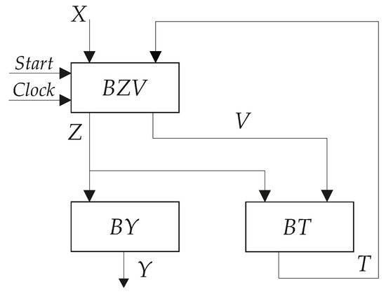
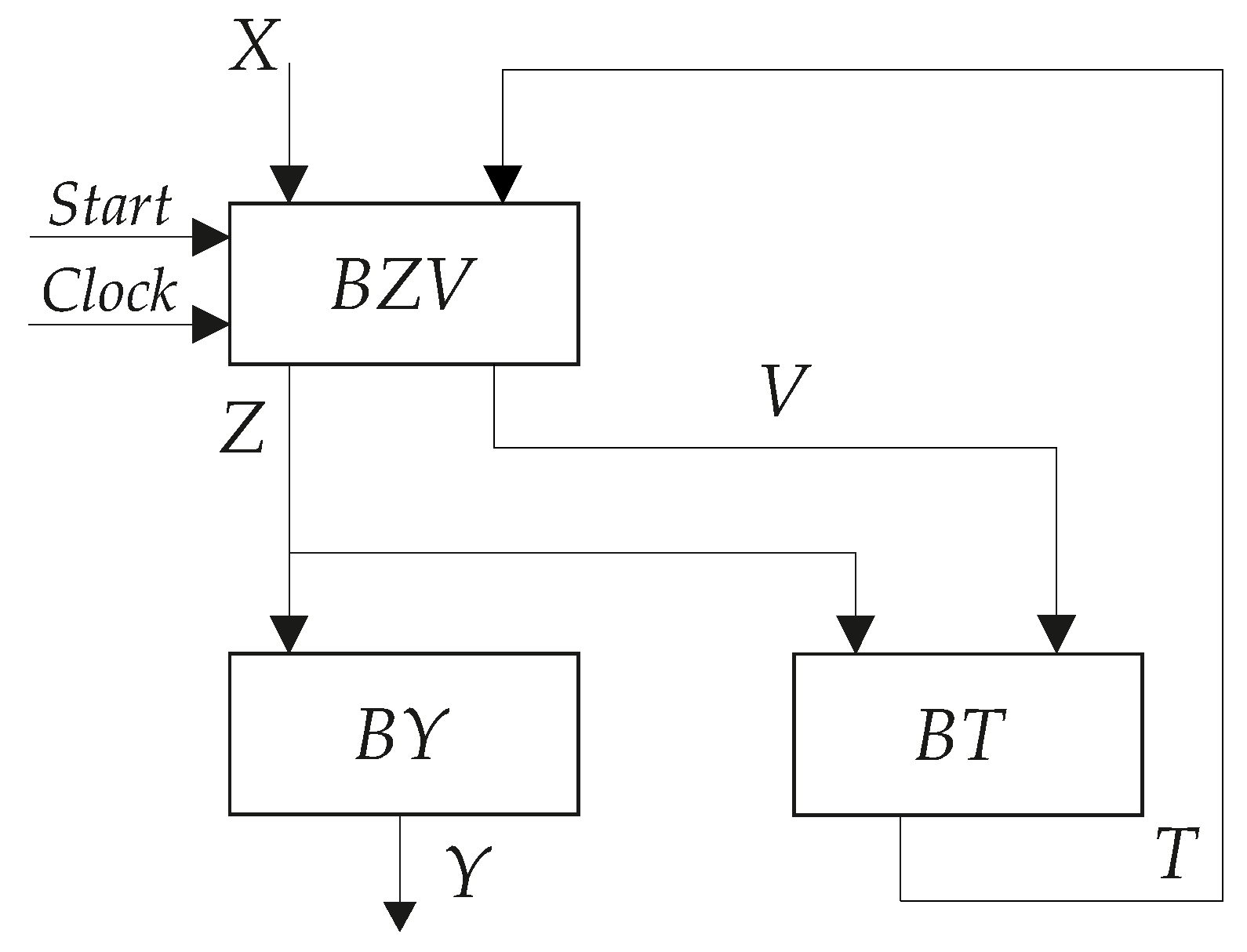
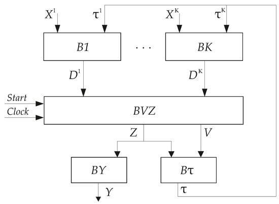
Figure 2.
Structural diagram of FSM .
Three blocks create this FSM circuit. The block generates functions belonging to SBFs (13) and (14). This block includes a hidden register having flip-flops. The variables and are registered because they correspond to outputs of flip-flops. The pulses Start and Clock control the register. The block implements SBF (7). The block implements SBF (12).
If conditions (8) and (9) take place, then this approach allows implementing -based Moore FSM circuits with fewer LUTs than their counterparts based on the model [47], and the best results are reached if the following condition holds:
As with all LUT-based models, the model has one serious drawback, which manifests itself if there are some states for which the following condition is true:
In (16), the symbol stands for the number of FSM inputs determining transitions from a state .
4. Essence of Proposed Method
To improve the basic characteristics of the Moore FSM circuit, we propose to transform the codes (11) into extended state codes (ESC) [3]. The extended state codes are based on finding a partition ... of the set A by the classes of compatible states. States are encoded as elements of classes . So, a state is encoded by a partial state code . The code includes bits, where
In (17), the symbol stands for the number of elements in the class . To take into account the relation , some code should be used. Due to it, 1 is added to . Let us point out that states are compatible if their presence in the same class does not increase the required number of LUT inputs beyond the value [3].
The state variables ... create partial codes for a particular class . The sets are combined into the set having state variables:
Concatenations of partial codes create extended state codes :
In (19), we use the subscripts to show that a particular partial code used to represent a state as an element of a class . The symbol * stands for the operation of concatenation of binary strings. We do not use these subscripts during the synthesis process.
The k-th class determines a block generating partial IMFs:
In (20), the symbol stands for a set of partial IMFs generated during transitions from the states , and the symbol stands for a set of FSM inputs causing transitions from the states . These K blocks create the first level of the proposed FSM architecture. Each block generates up to partial functions.
These PBFs should be combined together as disjunctions:
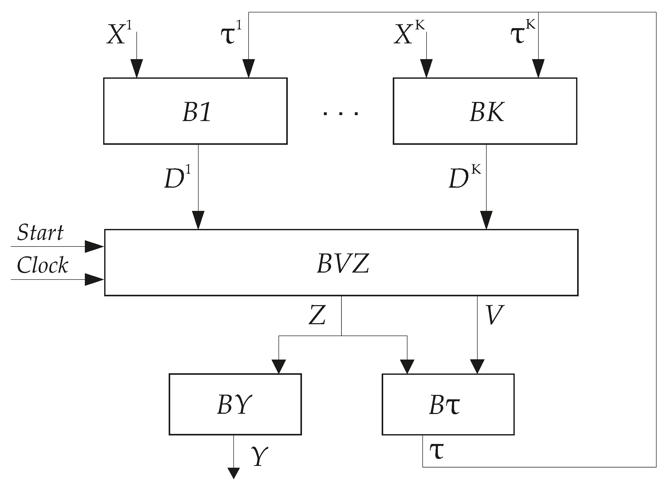
To generate functions , we propose to use a block . This is the second logic level of the FSM circuit. To transform (21) into stable variables and , the block should include a hidden register. There are flip-flops in this register. The variables are formed on the outputs of the first flip-flops. The variables are represented by the outputs of the last flip-flops. Obviously, these flip-flops should be controlled by synchronization and initialization pulses.
Two blocks of LUTs create the third circuit level. The block is a circuit generating FSM functions of SBF (7). The block generates expanded state codes as functions of additional variables and :
Using this preliminary information, we propose to represent a Moore FSM using the Moore FSM model . The proposed structural diagram is shown in Figure 3.
Figure 3.
Structural diagram of Moore FSM .
The principle of operation of is clear from the previous text. In this paper, we propose a method for synthesizing the LUT-based circuit for FSM . We assume that an FSM is representing its STT. If other representation forms are used, they should be converted to the equivalent STT. There are the following steps in the proposed method:
- 1.
- Splitting the set of states by K classes of compatible states.
- 2.
- Encoding of states by partial state codes .
- 3.
- Finding the output collections .
- 4.
- Encoding of output collections in a way that minimizes SBF (7).
- 5.
- Representing states by pairs <OC, identifier>.
- 6.
- Encoding the identifiers and creating FSM codes .
- 7.
- Constructing tables of blocks and finding SBFs (20).
- 8.
- Constructing the table of block and finding SBF (21).
- 9.
- Constructing the table of block and finding SBF (22).
- 10.
- Implementing the FSM logic circuit using the internal resources of a particular FPGA chip.
All steps of the proposed method have polynomial complexity with respect to the number of FSM states and transitions, and therefore can be efficiently applied to FSMs of practical size without introducing scalability limitations.
As follows from our previous research [36], an FSM could belong to a complexity group. There are three groups of FSMs (trivial, complex, and very complex). Of course, we still discuss FPGA-based Moore FSMs. For a particular FSM, the group can be determined using such parameters as R, L, , . All these parameters have been already determined.
For trivial FSMs, there is no sense in using decomposition methods. Their circuits contain exactly LUTs. As follows from [36], the trivial FSMs satisfy the following condition:
For very complex FSMs, the following condition holds:
For such FSMs, it is impossible to create the compatible classes of states. Because of the condition (24), LUTs do not have enough inputs for state variables. So, the FPGA-based circuits of very complex FSMs could be obtained using only FD-based methods.
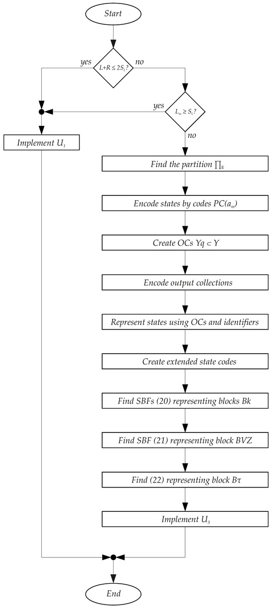
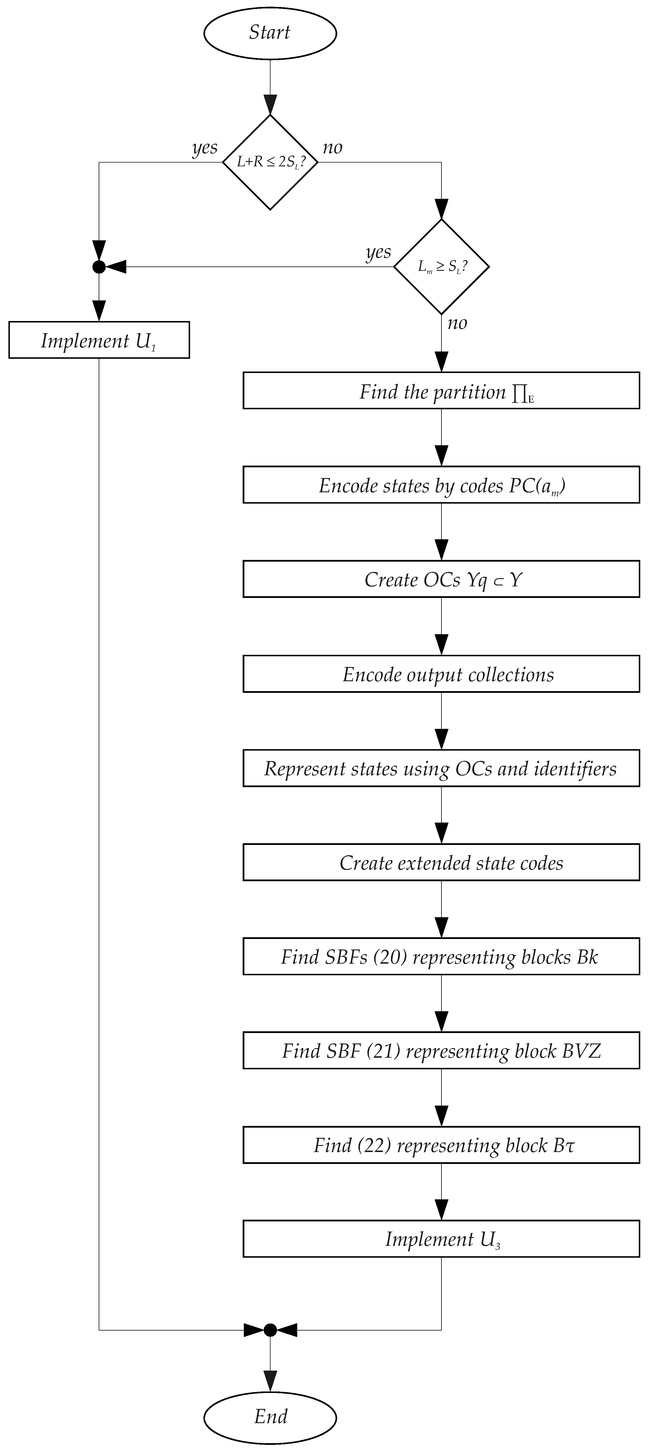
If conditions (23) and (24) are violated, SD-based methods can be used to optimize the spatial characteristics of FSM circuits. Such FSMs belong to the group of complex FSMs. So, our method deals with complex Moore FSMs. The method is represented by a flow-chart (Figure 4). We hope this flowchart will help to understand the sequence of steps in the proposed design method.
Figure 4.
Flowchart of the proposed method.
The first conditional node includes checking the condition (23). This is necessary to eliminate the trivial FSMs (output yes). If an FSM to be synthesized is not trivial (output no), then we should eliminate the very complex FSMs. This is checked using the condition (24) written in the second conditional node. The output yes shows that a particular FSM is very complex. The output no from the second conditional node indicates that a particular FSM is complex. So, it is necessary to execute the 10 steps shown in the operator nodes of the flowchart. These nodes include short commands taken from the list of steps shown above.
5. Example of Synthesis of Moore FSM
As shown in the results of the experiment (Section 6), this method should be used for rather complex FSMs. Such a complex example cannot be presented within the scope of this paper. Due to this, we show only the principle of synthesis in this section. Let us discuss how to synthesize a LUT-based circuit of rather simple FSM using the proposed method. To implement the FSM circuit, we use LUTs with inputs. The behavior of FSM Ex1 is represented by Table 2.
Table 2.
State transition table of Moore FSM Ex1.
The following sets could be derived from Table 2: ..., ... and .... So, the FSM has the following parameters: M = 10, L = 4, and N = 5. Table 2 includes H = 23 transitions .
Step 1. To find the partition , we use the greedy algorithm proposed in [47]. The main goal of the algorithm is to include as many possible states as possible into the classes .
The algorithm tries to minimize the number of FSM inputs determining transitions from states . As a result, the number of classes is minimized [47].
Using this approach in the discussed case, we can get the partition including classes: . Each class consists of five states: and . The transitions from states depend on FSM inputs . The transitions from states depend on FSM inputs .
Step 2. In the discussed case, each class includes five states: . Using (17) gives This determines the sets of partial state variables , . These sets form the set .... The states () are encoded by codes using variables from the set ().
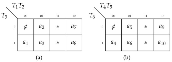
It is known [3] that partial state codes do not affect the number of LUTs in FSM circuit. So, we encode them as it is shown in Figure 5.
Figure 5.
Partial state codes for classes (a) and (b).
In Karnaugh maps (Figure 5), we use the symbol ∉ to show that this code is reserved for all states . This means that, for example, the following extended state codes can be obtained: , , , and so on.
Step 3. To create output collections , it is enough to analyze the column of the current state. In the discussed case, analysis of Table 2 allows getting the output collections , , , ,, and . This gives Using (5) gives . In turn, this defines a set . The variables are used to create codes .
Step 4. The OCs should be encoded in a way that minimizes the SOPs of the FSM outputs. This could be done, for example, using the approach from [62]. Let us create a system of relations between outputs and OCs. These relations are represented by disjunctions of OCs. The relation adds the term into the disjunction representing the output . In the discussed case, the following SBF represents these relations:
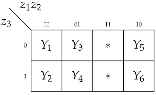
For example, as follows from Table 2, the output is produced if FSM Ex1 should generate collections . So, SBF (25) should include the equation All other Equation (25) are constructed in the same way. To minimize the number of literals in the SOP of , it is necessary to cover the codes , , and by the minimum possible number of generalized intervals of three-dimensional Boolean space. One of the possible outcomes of encoding is shown in Figure 6.
Figure 6.
Outcome of encoding of COs.
In the common case, using SBF similar to (25) and codes , SOPs for the system (7) could be created. Using SBF (25) and codes (Figure 6) gives the following system of SOPs:
Analysis of (26) shows that its SOPs include 8 literals. Each literal corresponds to a connection between some LUT input and a source of . So, the fewer literals in (7), the fewer interconnects an FSM circuit has. This allows reducing both the power consumption and required chip area [39].
In the worst case, the SBF (7) includes literals. In the discussed case, there is = 15. So, the proposed approach eliminates 7 literals (around 42% of literals).
The SBF (26) represents a circuit of . As we can see, three SOPs include only a single literal (SOPs for outputs ). So, to generate these outputs, there is no need for LUTs.
Step 5. To represent states using output collections and identifiers, it is necessary to analyze an STT. In our example, this is Table 2. For each OC , we should create a set . This set includes states in which a particular OC is generated. Analysis of Table 2 allows finding the following sets: , , , , , .
As follows from these sets, the maximum number of identifiers is equal to 2, whereas the minimum number is equal to 0. This analysis leads to the set of identifiers . Instead of pairs, we represent states as concatenations of OCs and identifiers. One of the possible variants is the following:
Step 6. There is . Using (10) gives . This determines the set . Let us encode identifiers in the trivial way: and . Using codes of OCs (Figure 6) and identifiers allows creating state codes (11). In the discussed case, we show codes in Table 3.
Table 3.
State codes for FSM Ex1.
In the common case, such a table has rows and M columns. The rows are marked by variables and . The columns are marked by the states of Moore FSM. The following codes, for example, are derived from Table 3: , , and so on. We use the symbol «x» to denote the insignificant bit of a particular code.
Step 7. Tables of blocks are constructed using the initial STT, partial state codes and state codes based on pairs <OC, identifier>. These tables consist of the following columns: , , , , , , h. There is no need to show OCs in the column of current state, because the system (7) is already created. Obviously, the relation ) is used to create the column of current states .
To create the table of (Table 4), it is necessary to use the rows 1–6 and 15–19 of STT (Table 2). The column is filled using the Karnaugh map (Figure 5a). To create the table of (Table 5), it is necessary to use the rows 7–14 and 20–23 of STT (Table 2). The column is filled using the Karnaugh map (Figure 5b).
Table 4.
Table of block .
Table 5.
Table of block .
These tables are used for deriving SBFs (20). Let us show only two partial IMFs, and . These partial IMFs are represented by the following SBF:
In (28), the symbol stands for a product term corresponding to the h-th line of a particular table. For example, the first line of Table 4 determines the term . The first line of Table 5 determines the term .
Step 8. The block includes both combinational part (LUTs) and memory (flip-flops of RG). The combinational part is a circuit generating IMFs (21). The memory part registered these functions, which represent additional variables and . A table of block has columns and K rows. The first column includes the classes . Other columns are marked by IMFs . If some IMF presents in the table of block , then the symbol «1» is written on the intersection of the row and the column . If some IMF is absent in the table of block , then the symbol «0» is written on the intersection of the row and the column . Analysis of Table 4 shows that its column includes all partial IMFs. The same is true for Table 5. Using this information, we can create the table of block for our example (Table 6).
Table 6.
Table of block .
Using Table 6 gives the final values of IMFs (21). The following system of disjunctions is constructed on the base of Table 6:
Step 9. The table of block shows the dependence between codes and extended state codes . This table should include the columns (all states are included in this column), , , (partial state variables equal to 1 in the extended state code from the line of the table), m. Using state codes (Table 3) and extended state codes (concatenations of partial codes from Karnaugh maps shown in Figure 5), we can create Table 7 representing the block .
Table 7.
Table of block .
Using Table 7 gives the following SOPs representing partial state variables:
Let us explain, for example, how the SOP of is created. This variable is written in rows 7 and 8 of Table 7. This gives the function , where the term is a conjunction of variables and (or their complements) corresponding to . To minimize this function, we should use the code 1000 for . This gives . Also, there is . The disjunction of these terms does not include the variable . This gives the final expression which is present in (30). In the same manner, all other equations from (30) are obtained.
Step 10. To implement an LUT-based FSM circuit using FPGAs from AMD Xilinx, we should use, for example, the industrial-grade Vivado [45]. This package does not support LUTs with . So, we have no way to show the outcome of the implementation in our example. But we present many outcomes in the next section.
6. Experimental Results
We investigated the efficiency of the proposed method using standard benchmarks from the library [63]. This library consists of 53 benchmark Mealy FSMs taken from the practice of logic design. These benchmarks are very often used by different researchers to compare new and known results [52,59,64]. The benchmarks are represented using KISS2 files. To conduct the research, we transform these files into equivalent Moore FSMs. The transformation was executed using approach [20]. In Table 8, the main characteristics of the obtained Moore FSMs are shown. The last column of Table 8 includes the result of the summation for the number of inputs and state variables.
Table 8.
Characteristics of Moore FSMs.
To translate KISS2 –based files into VHDL-based FSM models, we use our CAD tool K2F [47]. To synthesize and simulate FSMs, the Active-HDL environment is used. To get FSM circuits, we used Vivado v2025. 1 [45]. The FPGA chip Virtex7 Ultrascale+ xcvu29p-fsga2577-2L-e [41] was used as a target platform. This chip includes LUTs with 6 inputs. Eight such LUTs are placed into a single CLB. Using dedicated multiplexers, it is possible to create super-LUTs having either 7 (four 7-input LUTs), or 8 (two 8-input LUTs), or 9 inputs (one 9-input LUT). To create a 7-input LUT, the multiplexers F7 MUX are used. To create an 8-input LUT, the multiplexers F8 MUX are used. To create a 9-input LUT, the multiplexers F9 MUX are used.
We take three other methods to compare with the proposed approach. These methods are as follows: (1) Auto of Vivado; (2) One-hot of Vivado; (3) Gray of Vivado. The results of experiments are shown in Table 9 (Auto), Table 10 (One-hot), Table 11 (Gray), and Table 12 (). Each table contains the following columns: Benchmark, LUTs (the number of LUTs having 6 inputs), F7 MUX (the number of multiplexers used for creating super-LUTs with 7 inputs), F8 MUX (the number of multiplexers used for creating super-LUTs with 8 inputs), Registers (the number of D flip-flops used for creating the state register), Delay (the time of cycle), Freq. (the maximum operating frequency), Power (the value of consumed power).
Table 9.
Experimental results for Auto-based FSMs.
Table 10.
Experimental results for One-hot-based FSMs.
Table 11.
Experimental results for Gray-based FSMs.
Table 12.
Experimental results for -based FSMs.
Power consumption values were obtained using the standard power estimation flow provided by the Vivado design environment. The estimates were generated under uniform default assumptions regarding clock frequency, signal switching activity, and operating conditions, without applying benchmark-specific activity files or custom input vector activity. This methodology ensures consistent conditions across all evaluated benchmarks and synthesis variants, enabling a relative comparison of power trends across different FSM implementations. While absolute power values may vary depending on switching activity assumptions, the reported results are intended to illustrate comparative power behavior under identical estimation settings.
Using (23) and (24) allows dividing the benchmarks by three groups: trivial, complex, and very complex. For trivial benchmarks, the following condition takes place: . For complex FSMs, this condition is violated. However, the group of complex FSMs includes benchmarks that are too complex for our method. Our experience tells that these benchmarks include states for which the sum of significant FSM inputs exceeds the value of .
The group of complex FSMs includes the following benchmarks: ex1, kirkman, planet, planet1, pma, s1, s1488, s1494, s1a, s208, s298, styr, tma. The group of very complex FSMs includes the benchmarks s420, s510, s820, s832, sand, scf. All other benchmarks create the group of trivial FSMs. So, there are 13 complex FSMs, 6 very complex FSMs, and 34 trivial FSMs in the library [63].
There is no sense in using our method for trivial FSMs. For trivial benchmarks, it is better to use either One-hot- or Grey-based approaches. The same is true for very complex FSMs. The following rule is used to fill Table 12: for trivial and very complex FSMs, we should take the best results among either One-hot- or Grey-based approaches.
Using Table 9, Table 10, Table 11 and Table 12, we created Table 13, Table 14 and Table 15 to compare the basic characteristics of obtained circuits (the LUT count, operating frequency, and power consumed). These tables are organized in the same order. The rows are marked by benchmark names, and the columns by design methods. The row “Total” includes the sum of the corresponding values. The summarized characteristics of U3-based FSMs are taken as 100%. The row “Percentage” shows the percentage of summarized characteristics, respectively, to benchmarks based on U3.
Table 13.
Experimental results (LUT count).
Table 14.
Experimental results (maximum operating frequency, MHz).
Table 15.
Experimental results (power consumption, W).
As shown in Table 13, the U3-based FSMs required fewer LUTs than those for other investigated methods. There is the following economy: (1) 133% regarding Auto; (2) 29% regarding One-hot, and (3) 21% regarding Grey-based FSMs. As a rule, our approach gives better results for FSMs where condition (4) is violated and conditions (8) and (9) have places.
As shown in Table 14, the U3-based FSMs have a higher operating frequency than the other investigated methods. There is the following gain: (1) 10.6% regarding Auto; (2) 9.73% regarding One-hot, and (3) 4.28% regarding Gray-based FSMs. The gain is increased for complex FSMs. We think that, for complex FSMs, the proposed approach produces circuits with fewer levels and shorter interconnection networks.
Our approach allows producing circuits with a more regular interconnect system. Interconnections are known to be responsible for up to 70% of energy losses in FPGA-based circuits [26,65,66]. Due to the regularization of interconnections, our approach results in lower energy consumption than other investigated methods. As shown in Table 15, the One-hot-based FSMs consume less power than U3-based FSMs. But our method provides economy compared with both Auto-based (35.84%) and Gray-based (52.98%) FSMs.
Also, we created two tables that compare all FSM characteristics. Table 16 shows the comparison for all benchmarks. Table 17 shows a comparison for complex FSMs.
Table 16.
Total results for all benchmarks.
Table 17.
Total results for complex FSMs.
As shown in the comparison of Table 16 and Table 17, the One-hot-based FSMs are the winners in terms of power consumption. We think that this is connected with the fact that each state of One-hot-based FSMs is represented by an unique flip-flop. In our method, states are encoded to minimize the number of arguments in the Boolean functions representing FSM outputs.
But the proposed method provides the significant improvement for spatial (chip area occupied by FSM circuit) and frequency. As shown in Table 17, U3-based complex FSMs require fewer LUTs than those for other investigated methods. There is the following economy: (1) 150.61% regarding Auto; (2) 38.69% regarding One-hot and (3) 23.29% regarding Grey-based FSMs. Also, analysis of Table 17 shows that U3-based FSMs have a higher operating frequency than the other investigated methods. There is the following gain: (1) 30.25% regarding Auto; (2) 25.47% regarding One-hot and (3) 16.27% regarding Gray-based FSMs.
So, our approach improves both spatial and temporal characteristics of complex FSMs. If minimum power consumption is used as the criterion for optimality, then One-hot-based FSMs are preferable. But if minimizing either LUT count or cycle time is a main criterion, then our method should be used for complex FSMs. Of course, this conclusion is true only for benchmarks [63] and the device AMD Virtex™ UltraScale+™ 56G PAM4 VCU129 FPGA Evaluation Kit (Virtex7 Ultrascale+ xcvu29p-fsga2577-2L-e) [29,41]. It is almost impossible to make a similar conclusion for the general case. But our experiments show that the proposed approach can reduce the occupied chip area and improve the performance of complex FSMs.
Table 18 and Table 19 summarize the execution time and memory peak results measured for the Vivado FPGA design flow. The reported values include both the synthesis stage and the complete Vivado flow, which comprises synthesis and implementation (optimization, placement, and routing) for the target FPGA device (Virtex7 Ultrascale+ xcvu29p-fsga2577-2L-e) [29,41]. For each method, results are presented as average values per benchmark and as cumulative values aggregated across all benchmarks, allowing a direct comparison of individual benchmark costs and total computational effort. All experiments were performed using Xilinx Vivado v2025. 1 [45] on a workstation equipped with an Intel(R) Core(TM) i9-14900K processor, 64 GB of RAM, and running Windows 11 (version 25H2). Each benchmark was executed once using identical synthesis and implementation settings, with the maximum number of threads limited to eight via the set_param general. maxThreads 8.
Table 18.
Synthesis and Vivado flow execution times for the analyzed methods.
Table 19.
Peak memory consumption during synthesis and Vivado flow execution.
The observed differences between the analyzed methods are relatively small and remain within a narrow range for both execution time and memory peak values. Moreover, given the number and size of the analyzed benchmarks, differences of the order of minutes or seconds can be considered negligible in the context of the overall Vivado design flow execution.
7. Conclusions
One of the basic problems in FPGA-based FSM design is improving the spatial characteristics of FSM circuits. It is very important to find a solution with a minimum LUT count and escape the increasing cycle time. For complex FSMs, synthesis is connected with the decomposition of SBFs representing an FSM circuit. In this paper, we proposed a method based on the structural decomposition [3] of Moore FSM circuits. The proposed method uses output code collections to create partial state codes.
As the conducted experiments show, the proposed method results in circuits with better spatial (LUT count) and temporal (maximum operating frequency) characteristics than equivalent FSMs. These equivalent FSMs were designed using three state-encoding methods (Auto, One-hot, Gray). The improved characteristics are possible for rather complex FSMs for which the total number of FSM inputs and state variables is at least twice the number of inputs of the base LUT. In experiments, we used LUTs with six inputs.
So, the proposed state assignment method reduces the spatial characteristics and increases the FSM’s performance. Thus, the proposed method can be used for designing rather complex FSMs if the main optimality criterion for FSM circuits is minimum LUT count and cycle time. We think that this approach could be used when multiple FPGA-based accelerators are used in application-specific standard products (ASSP) chips [67,68]. In this case, it is necessary to use hardware–software interfaces to coordinate the interaction of microprocessors and accelerators [9]. Interface protocols are represented as finite-state machines. The ASSP chips possess limited resources of LUTs. So, for such solutions, reducing the LUT count in FSM circuits is very important.
As our experiments show, some FSMs include states for which the number of inputs determining interstate transitions exceeds the number of LUT inputs. We called such FSMs very complex. The proposed method cannot be applied to designing very complex FSMs. The solution to this problem is one of the directions of our future research. The second research direction is the use of AI tools [69,70,71] in the FPGA-based design of Moore FSMs.
Author Contributions
Conceptualization, A.B., L.T., and K.K.; methodology, A.B., L.T., and K.K.; software, A.B., L.T., and K.K.; validation, A.B., L.T., and K.K.; formal analysis, A.B., L.T., and K.K.; investigation, A.B., L.T., and K.K.; writing—original draft preparation, A.B., L.T., and K.K.; supervision, A.B. All authors have read and agreed to the published version of the manuscript.
Funding
This research received no external funding.
Institutional Review Board Statement
Not applicable.
Informed Consent Statement
Not applicable.
Data Availability Statement
The data presented in this study are available in the article.
Conflicts of Interest
The authors declare no conflicts of interest.
Abbreviations
The following abbreviations are used in this manuscript:
| CLB | configurable logic block |
| CO | collection of outputs |
| DST | direct structure table |
| ECO | extended codes of output collections |
| EOC | encoding of OC |
| ESC | extended state codes |
| FD | functional decomposition |
| FPGA | field-programmable gate array |
| FSM | finite state machine |
| IMF | input memory function |
| LUT | look-up table |
| MBC | maximum binary codes |
| OC | output collection |
| SBF | systems of Boolean functions |
| SD | structural decomposition |
| SOP | sum-of-products |
| STG | state transition graph |
| STT | state transition table |
References
- DeMicheli, G. Synthesis and Optimization of Digital Circuits; McGraw–Hill: New York, NY, USA, 1994. [Google Scholar]
- Minns, P.D.; Elliott, I. FSM-Based Digital Design Using Verilog HDL; John Wiley & Sons: Chichester, UK, 2008. [Google Scholar]
- Barkalov, A.; Titarenko, L.; Krzywicki, K. Logic Synthesis for FPGA-Based Mealy Finite State Machines: Structural Decomposition in Logic Design; Taylor & Francis Group, CRC Press: Boca Raton, FL, USA, 2024. [Google Scholar]
- Czerwinski, R.; Kania, D. Finite State Machine Logic Synthesis for Complex Programmable Logic Devices; Lecture Notes in Electrical Engineering; Springer: Berlin, Germany, 2013; Volume 231. [Google Scholar]
- Kubica, M.; Opara, A.; Kania, D. Logic synthesis for FPGAs based on cutting of BDD. Microprocess. Microsyst. 2017, 52C, 173–187. [Google Scholar] [CrossRef] [Scilit]
- Kubica, M.; Kania, D.; Kulisz, J. A technology mapping of FSMs based on a graph of excitations and outputs. IEEE Access 2019, 7, 16123–16131. [Google Scholar] [CrossRef] [Scilit]
- Opara, A.; Kubica, M.; Kania, D. Methods of improving time efficiency of decomposition dedicated at FPGA structures and using BDD in the process of cyber-physical synthesis. IEEE Access 2019, 7, 20619–20631. [Google Scholar] [CrossRef] [Scilit]
- Kubica, M.; Kania, D. Area-oriented technology mapping for LUT-based logic blocks. Int. J. Appl. Math. Comput. Sci. 2017, 27, 207–222. [Google Scholar] [CrossRef] [Scilit]
- Barkalov, O.; Titarenko, L.; Mazurkiewicz, M. Foundations of Embedded Systems; Studies in Systems, Decision and Control; Springer International Publishing: Cham, Switzerland, 2019; Volume 195. [Google Scholar]
- Esper, K.; Wildermann, S.; Teich, J. Automatic synthesis of FSMs for enforcing non-functional requirements on MPSoCs using multi-objective evolutionary algorithms. ACM Trans. Des. Autom. Electron. Syst. 2023, 28, 98. [Google Scholar] [CrossRef] [Scilit]
- Ganewattha, C.; Khan, Z.; Lehtomaki, J. Hardware-accelerated real-time drift-awareness for robust deep learning on wireless RF data. ACM Trans. Reconfig. Technol. Syst. 2023, 16, 19. [Google Scholar] [CrossRef] [Scilit]
- Jiang, P.; Yang, X.; Gagan, A. Combining SIMD and many/multi-core parallelism for finite-state machines with enumerative speculation. ACM Trans. Parallel Comput. 2020, 7, 15. [Google Scholar] [CrossRef] [Scilit]
- Hazzazi, M.; Budaraju, R.; Bassfar, Z.; Albakri, A.; Mishra, S. A finite state machine-based improved cryptographic technique. Mathematics 2023, 11, 2225. [Google Scholar] [CrossRef] [Scilit]
- Garcia-Vargas, I.; Senhadji-Navarro, R. A new approach for implementing finite state machines with input multiplexing. Electronics 2023, 12, 3763. [Google Scholar] [CrossRef] [Scilit]
- Trifan, M.; Ionescu, B.; Ionescu, D. A combined finite state machine and PlantUML approach to machine learning applications. In Proceedings of the 2023 IEEE 17th International Symposium on Applied Computational Intelligence and Informatics (SACI), Timisoara, Romania, 23–26 May 2023; pp. 631–636. [Google Scholar] [CrossRef] [Scilit]
- Wiseman, Y. High-Speed Architecture for Hybrid Arithmetic–Huffman Data Compression. Technologies 2025, 13, 585. [Google Scholar] [CrossRef] [Scilit]
- Salauyou, V.; Klimowicz, A.; Grzes, T. High-performance digital devices design by the ASMD-FSMD technique for implementation in FPGA. Appl. Sci. 2025, 15, 410. [Google Scholar] [CrossRef] [Scilit]
- Salauyou, V. Embedded processor design in FPGA by ASMD-FSMD and FSM-single techniques. In Proceedings of the 21st International Conference on Computer Information Systems and Industrial Management, Barranquilla, Colombia, 15–17 July 2022; pp. 374–389. [Google Scholar]
- Milik, A.; Kubica, M.; Kania, D. Reconfigurable logic controller—Direct FPGA synthesis approach. Appl. Sci. 2021, 11, 8515. [Google Scholar] [CrossRef] [Scilit]
- Baranov, S. Logic Synthesis for Control Automata; Kluwer Academic Publishers: Dordrecht, The Netherlands, 1994. [Google Scholar]
- Altera/Intel Corporation. Intel® FPGAs and Programmable Devices. Available online: https://www.intel.com/content/www/us/en/products/programmable.html (accessed on 15 January 2026).
- Atmel/Microchip Technology. Available online: https://www.microchip.com (accessed on 15 January 2026).
- AMD Xilinx. Available online: https://www.amd.com/ (accessed on 15 January 2026).
- Kuon, I.; Tessier, R.; Rose, J. FPGA architecture: Survey and challenges. Found. Trends Electron. Des. Autom. 2008, 2, 135–253. [Google Scholar] [CrossRef] [Scilit]
- Dhilleswararao, P.; Boppu, S.; Manikandan, M.S.; Cenkeramaddi, L.R. Efficient hardware architectures for accelerating deep neural networks: Survey. IEEE Access 2022, 10, 131788–131828. [Google Scholar] [CrossRef] [Scilit]
- Boutros, A.; Betz, V. FPGA architecture: Principles and progression. IEEE Circuits Syst. Mag. 2021, 21, 4–29. [Google Scholar] [CrossRef] [Scilit]
- Li, Z.; Zhang, Y.; Wang, J.; Lai, J. A survey of FPGA design for AI era. J. Semicond. 2020, 41, 021402. [Google Scholar] [CrossRef] [Scilit]
- Trimberger, S. Three ages of FPGA: A retrospective on the first thirty years of FPGA technology. Proc. IEEE 2015, 103, 318–331. [Google Scholar] [CrossRef] [Scilit]
- UltraScale™ Architecture and Product Data Sheet: Overview (DS890). Available online: https://docs.amd.com/v/u/en-US/ds890-ultrascale-overview (accessed on 15 January 2026).
- Grout, I. Digital Systems Design with FPGAs and CPLDs; Elsevier: Amsterdam, The Netherlands, 2011. [Google Scholar]
- Scholl, C. Functional Decomposition with Application to FPGA Synthesis; Kluwer Academic Publishers: Boston, MA, USA, 2001. [Google Scholar]
- Rawski, M.; Łuba, T.; Jachna, Z.; Tomaszewicz, P. The influence of functional decomposition on modern digital design process. In Design of Embedded Control Systems; Springer US: Boston, MA, USA, 2005; pp. 193–204. [Google Scholar]
- Lu, S.; Shang, L.; Qu, Q.; Jung, S.; Liang, Q.; Pan, C. An efficient multi-output LUT mapping technique for field-programmable gate arrays. Electronics 2025, 14, 1782. [Google Scholar] [CrossRef] [Scilit]
- Wang, F.; Zhu, L.; Zhang, J.; Li, L.; Zhang, Y.; Luo, G. Dual-output LUT merging during FPGA technology mapping. In Proceedings of the 39th International Conference on Computer-Aided Design (ICCAD), San Diego, CA, USA, 2–5 November 2020; pp. 1–9. [Google Scholar]
- Barkalov, A.; Titarenko, L.; Krzywicki, K. Reducing LUT count for FPGA-based Mealy FSMs. Appl. Sci. 2020, 10, 15. [Google Scholar] [CrossRef] [Scilit]
- Barkalov, A.; Titarenko, L.; Chmielewski, S.; Mielcarek, K. Improving characteristics of LUT-based Moore FSMs. IEEE Access 2020, 8, 155306–155318. [Google Scholar] [CrossRef] [Scilit]
- Chapman, K. Multiplexer design techniques for datapath performance with minimized routing resources. Xilinx All Program. 2014, 1, 1–32. [Google Scholar]
- Kilts, S. Advanced FPGA Design: Architecture, Implementation, and Optimization; Wiley-IEEE Press: Hoboken, NJ, USA, 2007. [Google Scholar]
- Feng, W.; Greene, J.; Mishchenko, A. Improving FPGA performance with a S44 LUT structure. In Proceedings of the 2018 ACM/SIGDA International Symposium on Field-Programmable Gate Arrays (FPGA’18), Monterey, CA, USA, 25–27 February 2018; pp. 61–66. [Google Scholar] [CrossRef] [Scilit]
- Murray, K.E.; Petelin, O.; Zhong, S.; Wang, J.M.; Eldafrawy, M.; Legault, J.-P.; Sha, E.; Graham, A.G.; Wu, J.; Walker, M.J. VTR 8: High-performance CAD and customizable FPGA architecture modelling. ACM Trans. Reconfig. Technol. Syst. 2020, 13, 9. [Google Scholar] [CrossRef] [Scilit]
- AMD. AMD Virtex™ UltraScale+™ 56G PAM4 VCU129 FPGA Evaluation Kit. Available online: https://www.amd.com/en/products/adaptive-socs-and-fpgas/evaluation-boards/vcu129.html (accessed on 15 January 2026).
- Baranov, S. Finite State Machines and Algorithmic State Machines; Amazon: Seattle, WA, USA, 2018. [Google Scholar]
- Sentovich, E.M.; Singh, K.J.; Moon, L.L.C.; Murgai, R.; Saldanha, A.; Savoj, H.; Stephan, P.R.; Brayton, R.K.; Sangiovanni-Vincentelli, A. SIS: A System for Sequential Circuit Synthesis; Technical Report UCB/ERL M92/41; University of California: Berkeley, CA, USA, 1992. [Google Scholar]
- Brayton, R.; Mishchenko, A. ABC: An academic industrial-strength verification tool. In Computer Aided Verification; Touili, T., Cook, B., Jackson, P., Eds.; Springer: Berlin/Heidelberg, Germany, 2010; pp. 24–40. [Google Scholar]
- Vivado Design Suite: Synthesis User Guide UG901 (v2025.1). Available online: https://docs.amd.com/r/en-US/ug901-vivado-synthesis/Introduction (accessed on 15 January 2026).
- Intel/Quartus. Quartus Prime Overview. Available online: https://www.intel.com/content/www/us/en/software/programmable/quartus-prime/overview.html (accessed on 15 January 2026).
- Barkalov, A.; Titarenko, L.; Mielcarek, K.; Chmielewski, S. Logic Synthesis for FPGA–Based Control Units: Structural Decomposition in Logic Design; Lecture Notes in Electrical Engineering; Springer: Berlin, Germany, 2020; Volume 636. [Google Scholar]
- Kubica, M.; Opara, A.; Kania, D. Technology Mapping for LUT-Based FPGA; Springer: Berlin/Heidelberg, Germany, 2021. [Google Scholar]
- Hierons, R.M.; Mousavi, M.R. Complete FSM Testing Using Strong Separability. arXiv 2025, arXiv:2502.04035. [Google Scholar] [CrossRef] [Scilit]
- Barkalov, A.; Titarenko, L.; Bieganowski, J.; Krzywicki, K. Basic approaches for reducing power consumption in finite state machine circuits—Review. Appl. Sci. 2024, 14, 2693. [Google Scholar] [CrossRef] [Scilit]
- Machado, L.; Cortadella, J. Support-Reducing Decomposition for FPGA Mapping. IEEE Trans.-Comput.-Aided Des. Integr. Circuits Syst. 2020, 39, 213–224. [Google Scholar] [CrossRef] [Scilit]
- Opara, A.; Kubica, M.; Kania, D. Decomposition approaches for power reduction. IEEE Access 2023, 11, 29417–29429. [Google Scholar] [CrossRef] [Scilit]
- Salauyou, V.; Bułatow, W. Optimized sequential state encoding methods for finite-state machines in field-programmable gate array implementations. Appl. Sci. 2024, 14, 5594. [Google Scholar] [CrossRef] [Scilit]
- Barkalov, A.; Titarenko, L.; Krzywicki, K. Improving characteristics of LUT-based sequential blocks for cyber-physical systems. Energies 2022, 15, 2636. [Google Scholar] [CrossRef] [Scilit]
- Testa, E.; Amaru, L.; Soeken, M.; Mishchenko, A.; Vuillod, P.; Luo, J.; Casares, C.; Gaillardon, P.; De Micheli, G. Scalable Boolean methods in a modern synthesis flow. In Proceedings of the 2019 Design, Automation and Test in Europe Conference and Exhibition (DATE), Florence, Italy, 25–29 March 2019; IEEE: New York, NY, USA, 2019; pp. 1643–1648. [Google Scholar]
- Xilinx. XST User Guide. Available online: https://docs.amd.com/v/u/en-US/xst_v6s6 (accessed on 15 January 2026).
- Vivado. Available online: https://www.amd.com/en/products/software/adaptive-socs-and-fpgas/vivado.html (accessed on 15 January 2026).
- Intel. Quartus II. Available online: https://www.altera.com/products/development-tools (accessed on 15 January 2026).
- Salauyou, V. Area and performance estimates of finite state machines in reconfigurable systems. Appl. Sci. 2024, 14, 11833. [Google Scholar] [CrossRef] [Scilit]
- Baranov, S. Logic and System Design of Digital Systems; TUT Press: Tallinn, Estonia, 2008. [Google Scholar]
- Xilinx. Virtex-7 T and XT FPGAs Data Sheet (DS183). Available online: https://docs.xilinx.com/v/u/en-US/ds183_Virtex_7_Data_Sheet (accessed on 15 January 2026).
- Achasova, S. Synthesis algorithms for automata with PLAs; Soviet Radio: Moscow, Russia, 1987. (In Russian) [Google Scholar]
- McElvain, K. LGSynth93 Benchmark; Mentor Graphics: Wilsonville, OR, USA, 1993. [Google Scholar]
- Opara, A.; Kubica, M. Technology mapping of multi-output functions leading to the reduction of dynamic power consumption in FPGAs. Int. J. Appl. Math. Comput. Sci. 2023, 33, 267–284. [Google Scholar] [CrossRef] [Scilit]
- Wang, X.; Stroobandt, D. Dense or Sparse? Post-Packing Interconnection Analysis in FPGAs. In Proceedings of the 15th International Symposium on Highly Efficient Accelerators and Reconfigurable Technologies (HEART’25), Kumamoto, Japan, 26–28 May 2025; pp. 142–146. [Google Scholar]
- Wang, X.; Stroobandt, D. The influence of interconnection complexity on the FPGA CAD flow. In Proceedings of the 2024 ACM International Workshop on System-Level Interconnect Pathfinding (SLIP ’24), Newark, NJ, USA, 31 October 2024. [Google Scholar]
- Marzuki, A. CMOS Analog and Mixed-Signal Circuit Design: Practices and Innovations; CRC Press: Boca Raton, FL, USA, 2020. [Google Scholar] [CrossRef] [Scilit]
- Rudan, M.; Brunetti, R.; Reggiani, S. Springer Handbook of Semiconductor Devices; Springer: Cham, Switzerland, 2023. [Google Scholar]
- Lin, C.; Yi, Y. Enhancing FPGA CAD Flow with AI-Powered Solutions. In AI-Enabled Electronic Circuit and System Design: From Ideation to Utilization; Springer Nature: Cham, Switzerland, 2024; pp. 225–256. [Google Scholar] [CrossRef] [Scilit]
- Namboothiripad, M.K.; Vadhyan, G. Efficient implementation of artificial neural networks on FPGAs using high-level synthesis and parallelism. Int. J. Adv. Technol. Eng. Explor. 2024, 11, 1497. [Google Scholar] [CrossRef] [Scilit]
- Seo, J.; Park, S.; Kang, S. Unveiling the Black-Box: Leveraging Explainable AI for FPGA Design Space Optimization. In Proceedings of the 2024 Design, Automation & Test in Europe Conference & Exhibition (DATE), Valencia, Spain, 25–27 March 2024; IEEE: Piscataway, NJ, USA, 2024; pp. 1–6. [Google Scholar]

Disclaimer/Publisher’s Note: The statements, opinions and data contained in all publications are solely those of the individual author(s) and contributor(s) and not of MDPI and/or the editor(s). MDPI and/or the editor(s) disclaim responsibility for any injury to people or property resulting from any ideas, methods, instructions or products referred to in the content. |
© 2026 by the authors. Licensee MDPI, Basel, Switzerland. This article is an open access article distributed under the terms and conditions of the Creative Commons Attribution (CC BY) license.