Abstract
Junction temperature is considered a critical parameter that can directly affect the reliability and power handling capabilities of semiconductor devices. Effective thermal management, particularly under high-surge-current conditions, is therefore essential to maintain a lower junction temperature in order to enhance device performance and prevent device failure. Among various thermal management strategies, packaging technology plays an important role in optimizing junction temperature and enhancing the robustness of the device. In this article, a comparative analysis of high-power diodes is performed by investigating their junction temperature behavior and surge current handling capability. Moreover, an insulated module diode and a press-pack diode with pressure contact technology (PCT), both with identical specifications and power ratings, are selected for analysis. A 10 ms half-sine surge current waveform generator is developed both experimentally and in simulations to replicate realistic surge events. Experimental measurements of the forward voltage drop across varying surge levels are used to analyze device failure behavior. In addition, electro-thermal simulations are also employed in PSIM 2025.0 software to estimate and compare the temperature. Furthermore, this study enables practical insights into device thermal performance, robustness, and surge current handling capabilities, enabling a performance comparison between the two packaging technologies.
1. Introduction
Junction temperature is considered a critical parameter for evaluating the performance and reliability of semiconductor devices, especially high-power thyristors, diodes, and IGBTs. These devices play a crucial role in power electronics applications, such as high-voltage direct currents (HVDCs) [1,2], fast charging electric vehicles [3,4], hydrogen electrolysis, traction power supply, voltage regulation and conversion, and multi-level converters [4,5], where they operate under high-voltage and current conditions. The increasing demand for high power densities in these applications has motivated manufacturers to develop advanced power semiconductor devices with improved designs and new packaging techniques to optimize power dissipation to meet the required power ratings. However, an increase in current beyond specified limits may trigger more power, which may increase the temperature and induce electro-thermal and associated stresses in a device [6,7]. Therefore, accurate estimation of the junction temperature is essential for optimizing power dissipation, preventing performance degradation, improving reliability, and increasing lifespan by ensuring operation within specified thermal limits. Among the many other factors influencing thermal resistance and impedance, including material composition, geometry, and contact surface quality, the junction temperature can be optimized through appropriate device architecture and packaging design, as shown in Table 1, alongside effective thermal management.

Table 1.
Technological aspects of high-power semiconductor devices.
High-power semiconductor devices have traditionally been implemented using insulated module-based architectures, as illustrated in Figure 1, using brazing and welding contact technology, where a semiconductor chip and multiple layers of various materials (Si, ALN, ALSiC, Copper) are connected together and to external electrodes via soldering and welding wires. However, this packaging approach supports only low- to medium-current operations because heat flows (Q) through a single conduction path from the chip to the heat sink before being dissipated to ambient . This limited thermal pathway reduces reliability, and long-term operation is often compromised due to degradation mechanisms such as bonding wire lift-off and solder joint cracking, which lead to performance degradation and eventual device failure [8,9].
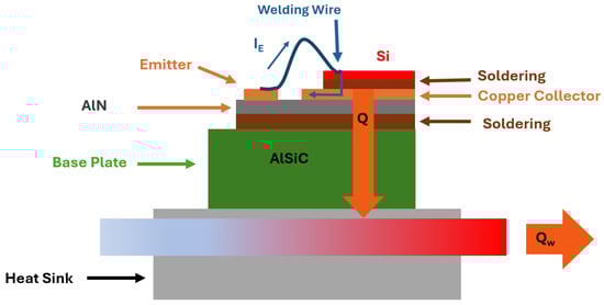
Figure 1.
Structure and heat transfer mechanism of a conventional brazed and welded contact module.
With advancements in packaging technology, PCT has been re-established and extended to various configurations, including insulated modules and press-pack ceramic housing assemblies, as shown in Figure 2 and Figure 3, respectively. In these devices, multiple layers are stacked together by clamping force, ensuring direct electrical and thermal contact without the need for wire bonds or solder joints. Moreover, in switching devices, such as thyristors, IGBTs, etc., the gate connections to the terminals are replaced by gate springs. The gate springs make them more reliable and robust to performance degradation and failure. Insulated module assemblies commonly employ monolithic, silicon, and round-shaped diodes and thyristors. This configuration enhances the device reliability and supports medium to high current ratings, while reducing the risk of failure by eliminating soldered interconnections. For applications with very high currents, the use of PCT in press-pack ceramic housing designs further improves reliability and thermal performance. This configuration enables two-sided cooling, supported by heat sink A and heat sink B, with corresponding heat dissipation paths and respectively, as depicted in Figure 3 [10]. However, increased current levels from anode (A) to cathode (K) beyond specified limits can make all these packaging configurations susceptible to failures, such as fretting damage, micro-eroding, and spring fatigue.
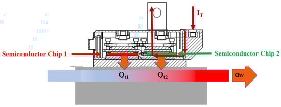
Figure 2.
Schematic of the structure and heat transfer mechanisms of the PCT insulated module.
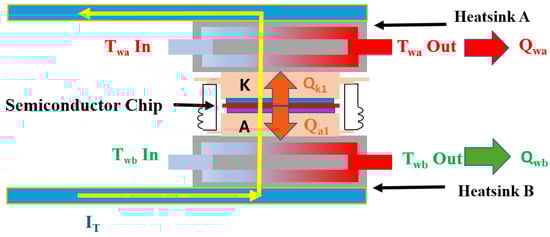
Figure 3.
Schematic illustration of the structure and heat transfer mechanisms in the PCT press-pack diode.
Additionally, press-pack devices lack encapsulation, decreasing the risk of chip rupture and explosion under fault conditions. These failures are primarily driven by excessive junction temperatures caused by surge currents and thermal cycling, inducing thermo-mechanical stresses that ultimately compromise device reliability [6]. In the existing literature, surge current capability of power devices is typically evaluated at relatively low current levels ranging from several amperes such as 50 A [11], 110 A [12], and 400 A [13] to several hundred amperes, such as 1200 A [14] and 1500 A [15], which is insufficient for practical high-power applications, where devices experience very high fault currents (several kA), leading to high temperature increase and overheating. Therefore, it is essential to assess surge current limits at significantly higher levels to ensure reliable operation. The main contributions of this paper are summarized as follows:
- A comparative analysis is conducted between a PCT press-pack diode and a PCT insulated module diode, with both having identical silicon chip dimensions, electrical specifications, and power ratings, under high-surge current conditions.
- A 10 ms high half-sine surge current waveform generator is developed both experimentally and in PSIM to analyze surge events at different power levels for both diode packaging types.
- Simulations were performed to estimate junction temperatures by utilizing measured currents and voltages.
- The estimated junction temperature is evaluated by an electro-thermal model in order to study the behavior of the device during high-stress surge conditions.
- Failure mechanisms and thermal limitations are investigated to assess the robustness and surge current handling capabilities of both diode technologies.
- The findings offer practical guidance on the thermal–electrical trade-offs between press-pack and insulated module diodes for use in high-power applications.
The rest of paper is structured as follows: In Section 2, different failure modes are discussed. Section 3 presents the device structure and thermal modeling methodology. Section 4 introduces the experimental setup and results. The simulation setup is discussed in Section 5, followed by simulation results in Section 6. Section 7 discusses device failure mechanisms. Finally, Section 8 concludes the study by summarizing key findings and implications.
2. Failure Modes
Failure behavior in semiconductor devices primarily occurs due to elevated junction temperatures, which arise from multiple interacting factors, as given in Figure 4. These failure mechanisms have been discussed in [16,17,18]. They typically result in material degradation, interconnect fatigue, solder fatigue and delamination, or cracking of critical device regions, especially the chip. Failures that arise due to packaging and material stresses usually originate at interfaces such as the die attach, bond wires, substrates, and molding compounds. Mismatches in the Coefficient of Thermal Expansion (CTE) between two dissimilar materials induce thermo-mechanical stresses due to thermal or power cycling, which can lead to interfacial cracking, delamination, or bond-wire lift-off.
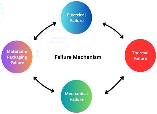
Figure 4.
Notable factors that impact device reliability and cause device degradation and failure.
Voids or delamination in solder and die attach layers also increase thermal resistance, resulting in localized hot spots and accelerated degradation [19,20,21]. Failures that are initiated due to mechanical stresses are usually driven by external perturbations such as vibration, shock, or handling stress [22,23]. Encapsulation-induced stress can also contribute significantly, where uneven stress distribution in molding compounds causes die cracking or initiates delamination at weak interfaces [24]. Failures that occur due to thermal stresses are primarily associated with a rise in temperature, gradients, as well as thermal cycling [25]. Repeated thermal cycling induces fatigue in solder joints and bond wires, while localized hot spots cause differential expansion and accelerate crack propagation. At elevated temperatures, creep in the solder and die attach layers further compromises structural and thermal integrity. In extreme cases, a positive feedback between temperature rise and leakage currents may initiate thermal runaway, culminating in catastrophic device failure. Failures that occur due to electrical overstress are usually triggered by conditions such as an increased blocking voltage, higher surge current levels, and over-voltage transients [26,27]. Apart from this, other mechanisms include thermal fatigue during fast commutation, avalanche breakdown, and gate oxide degradation. Mostly these failures occur abruptly, leading to immediate device destruction. While robust protection circuits can reduce the risk, they may not prevent irreversible damage. Electrical overstress can result in increased leakage current and forward voltage drop, which may lead to short-circuit conditions, metallization melting, or even chip fracture [19]. Moreover, PCT devices also eliminate traditional bond-wire and solder-related degradation by relying on direct contact between the die and electrodes. However, failures in these devices still arise due to interface-degradation-associated instabilities, as detailed in Table 2. Primary failure mechanisms include fretting damage, micro-eroding, gate oxide damage, spring fatigue, and stress relaxation [28,29]. In welding and brazed diodes, the failure mechanism of bond wire lift-off can lead to an open-circuit condition, which may generate an arc. The resulting electric shock can trigger an explosion outside the device, posing hazards to the external environment. In contrast, PCT diodes contain no bond wires; therefore, under high-current and voltage conditions, failure manifests as a short circuit, leading to elevated temperatures and eventual chip fracture rather than arc formation. All failure phenomenon are monitored using prognostics and health management techniques through various health indicators such as on-state voltage [30,31], threshold voltage [32], switching waveforms [33], case temperature [34], and thermal impedance [35]. Notably, and can distinguish between bond-wire lift-off and solder layer degradation, enabling detailed failure mechanism analysis.
Table 2.
Failure mechanism in PCT devices, both press-pack and PCT insulated modules.
Bond-wire lift-off is monitored by measuring the relative health indicator at a fixed junction temperature, although this requires precise and power loss measurements [36,37,38]. is also proposed as an indicator for solder layer degradation; however, sensor placement between the case and heatsink can impact heat dissipation efficiency [34]. Alternative approaches use on-state voltage and bond-wire voltage drop as damage indicators—on-state voltage for temperature estimation, predicting solder joint failures that increase thermal resistance, and bond-wire voltage drop to detect bond-wire degradation [39].
The degradation of wire metallization interfaces can also lead to damage of wire bonds and eventual contact loss with the metallization pad [40,41]. Various models, including physical and analytical approaches, have been developed to predict wire bond degradation and assess device reliability. In [42], a temperature-variation-based model was proposed to evaluate the influence of time at temperature on degradation processes. These failure modes, as well as performance degradation, lifetime prediction, and aging analysis, are discussed in detail in [9,26,27,28,29]. In these studies, critical insights into device failure mechanisms are provided that can affect performance and reliability. Moreover, improved encapsulation results in longer lifetimes, and an increase in temperature still remains a significant challenge; hence, further research is required to advance packaging techniques and optimize thermal management strategies to address thermal stress under harsh operating conditions. The failure of a single device can compromise the safety and reliability of an entire system, particularly in configurations where multiple devices are interconnected. Therefore, studying the thermal behaviour of each component is crucial for ensuring system protection and cost efficiency. A detailed analysis of the thermal behavior of semiconductor devices provides critical insights into heat flow distribution across different regions. For example, in high-power diodes, the silicon chip is susceptible to thermal degradation due to surge currents. Other factors, including repeated overstresses and thermal or power cycling, may also influence device performance. However, effective thermal analysis enables the identification of uneven current distribution, which can induce localized hot spots and junction temperature fluctuations, leading to excessive thermal loading and accelerated device failure.
3. PCT Device Structure
A typical power semiconductor packaging design for high-power PCT insulated module diodes and advanced PCT press-pack diodes consists of a multilayer structure with different materials, as shown in Figure 5.
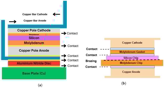
Figure 5.
Device structure. (a) PCT insulated module diode. (b) PCT press-pack diode.
These configurations are analyzed and compared to determine the thermal performance of different packaging designs under higher-current events with extreme thermal conditions. The insulated module diode structure consists of a silicon chip interfaced with copper anodes and cathode electrodes via molybdenum contact layers to optimize electrical and thermal performance. Copper reinforcement bars are employed at both electrode terminals, as depicted in Figure 5a, to ensure the flow of the current from the anode toward the junction. On the anode side, an aluminum nitride disc is also incorporated between the reinforcement bar and the copper base plate, thus enabling electric isolation, to avoid any electric discharge from the chip and any other metallic part to the base plate. The cathode side mirrors the anode architecture, maintaining the copper reinforcement bar to ensure electric current symmetry, but omitting the aluminum nitride disc. In contrast, press-pack diodes interface the silicon junction with the copper anode and cathode electrodes through intermediate molybdenum layers, as shown in Figure 5b. However, they lack copper reinforcement bars and aluminum nitride discs and rely on brazed joints between the silicon chip and molybdenum layers to achieve mechanical stability. The device exhibits a symmetrical heat dissipation pattern, with heat generated at the center and propagating equally toward the anode and cathode sides. Heat flow from the silicon junction to the external terminals is influenced by various factors, including thermal properties, geometry, and dimensions of the adjacent layers. Thus, the generated heat ultimately dissipates to the ambient environment through the device case and heat sink. Furthermore, the overall thermal capability in both assemblies is significantly influenced by the thermal contact resistances at each material’s interface, where mismatches in material properties introduce additional thermal barriers. The thermal resistance Rth and thermal capacitance Cth of each layer depend on both geometric parameters and material properties. Precise measurement and comprehensive data of materials play a crucial role in determining a better transient thermal response of the device, and can be obtained as follows:
where d is the layer thickness, is the thermal conductivity, is the material density, is the specific heat capacity, and is the effective area at thickness z.
4. Experimental Setup and Results
4.1. Experimental Test Setup
Experimental tests were carried out on a PCT press-pack diode and a PCT insulated diode model, both from the same manufacturer and unused, with ratings of 4400 V and 4500 V, respectively. The devices had similar specifications and featured chip diameters of 48 mm. The experimental setup, designed in accordance with the IEC 60747–2 standard [43], as illustrated in Figure 6, is designed to generate controlled surge current pulses using a single-phase full-wave rectifier connected to a transformer Tx1 via a resistor R1 and an inductor. The surge current, as shown in Figure 7, ranging from 6400 A to 36,700 is generated through a resistor–capacitor (RC) charge–discharge mechanism. To mitigate the risk of explosion at very high currents, the equipment is enclosed with a protective grille, as illustrated in Figure 8. Moreover, an external DC power supply charges the capacitor C1, while the flow of the current is regulated by a set of thyristors X1, X2, X3, and X4.
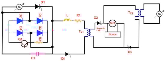
Figure 6.
Schematic representation of experimental surge test setup.
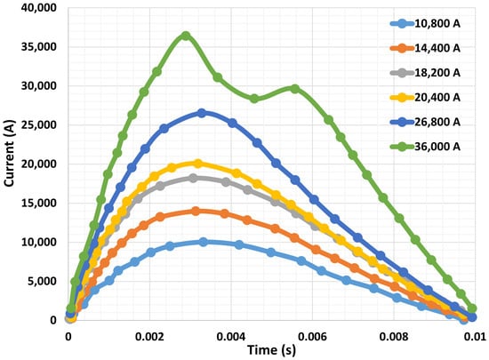
Figure 7.
Surge current waveforms for the performed experimental surge tests.
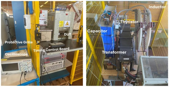
Figure 8.
Experimental bench setup for surge current test.
Thyristor X1 governs the charging of C1, enabling precise control over the starting and disengaging of the capacitor charge. For the positive half-cycle of the AC supply, thyristors X2 and X4 are triggered, which initiates current flow through the capacitor and inductor. At the zero-crossing point, which marks the start of the negative half-cycle, thyristor X3 is activated. As the current decreases, X2 automatically turns off, leading to polarity reversal across C1. The stored energy is then discharged through a Device Under Test (DUT), which completes the surge event. Current measurements are obtained using a Rogowski coil placed on the primary side of the transformer . Surge events are configured for a 10 ms duration using a dedicated timing control board, as shown in Figure 8. All relevant electrical parameters are captured via a four-channel digital oscilloscope, which ensures synchronized and accurate waveform acquisition.
4.2. Experimental Results
A series of surge current tests was performed experimentally, as discussed in Section 4.1. The test started at a lower-level current, having a peak amplitude of 6.4 kA and gradually increased until device failure. For each surge level, the corresponding forward voltage drop was recorded to monitor the electrical response of the device, as shown in Figure 9 and Figure 10. After the surge test, electrical tests were carried out that confirmed that the diode’s electrical characteristics were only slightly changed compared to prior characteristics, confirming no performance degradation or failure in the device.
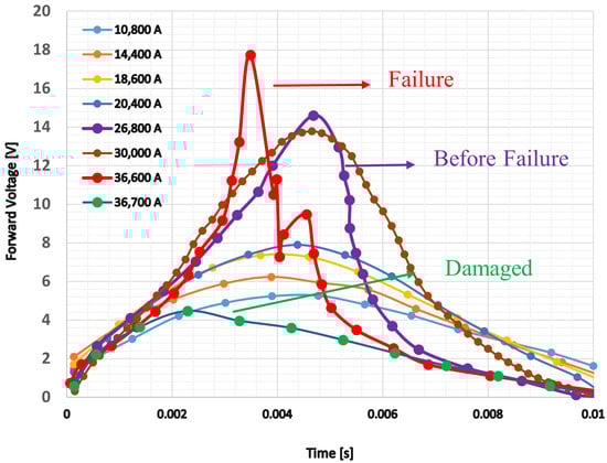
Figure 9.
Measured voltages for PCT press-pack diode.
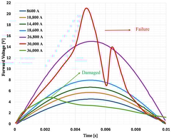
Figure 10.
Measured voltages for PCT insulated module diode for corresponding surge currents.
Furthermore, the PCT press-pack diode demonstrated robust performance under high-surge-current conditions, withstanding peak currents of up to 36 kA, approximately 11 times its nominal current rating, without failure. However, irreversible failure was noted after this, thereby defining the threshold of surge currents under the specified test parameters. Moreover, prior to device failure, at a surge current of 30 kA, metallization of aluminum nitride was observed, indicating the start of performance degradation. The module diode, on the other hand, showed metallization evaporation at 26.8 kA, while a chip failure occurred at a lower current level of 30 kA.
These results show that the PCT press-pack device is capable of handling better surge currents than the insulated module diode. Additionally, it also provides critical insight into their respective failure mechanisms under higher surge current, as discussed in Section 7. These results clearly demonstrate that the insulated module diode exhibits higher thermal resistance, resulting in a greater voltage drop and a more rapid temperature rise, as a result of its limited power dissipation capability, and thus, the reliability of the device at higher current levels is compromised.
Numerical Acquisition and Processing
The current and voltage waveforms, recorded by a digital four-channel oscilloscope, during the experimental tests, as represented in Figure 11 and discussed in Section 4.2, were exported as numerical datasets. These waveforms were subsequently imported into Python 3.13 for quantitative analysis and preliminary power calculations, as shown in Figure 12a. The instantaneous power, capturing both the peak values and the total pulse energy, can be given as follows:
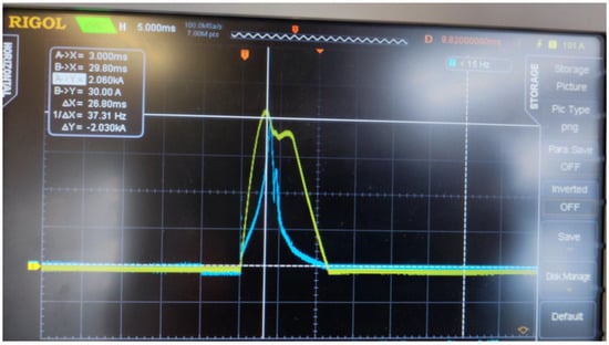
Figure 11.
Current and voltage waveforms recorded during the experiment using an oscilloscope.
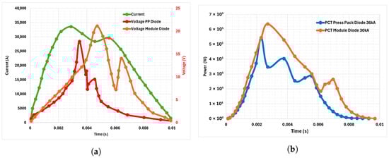
Figure 12.
Parameter waveforms during surge operation. (a) Measured current and voltage waveforms. (b) Acquired time-dependent power based on corresponding electrical parameters.
The resulting time-dependent power profiles were then used as inputs for the thermal model described in Section 5, enabling accurate prediction of the transient temperature evolution under the same operating conditions as the experiment. The instantaneous power can be modeled as
where is the peak amplitude of power, T is the total pulse duration, and t is the instantaneous time at which power is evaluated. The first term represents the fundamental sinusoidal behavior of the surge waveform over the time period T. Moreover, the second term introduces a Gaussian dip, implemented as an exponential modulation, which locally attenuates the power around . is the time shift that indicates the occurrence time of the dip. The attenuation coefficient controls the depth of the dip, while its temporal spread is determined by . This expression captures deviations from an ideal sinusoidal surge, accounting for non-ideal damping and transient thermal–electrical interactions, thereby providing a power profile that closely matches experimental results, as shown in Figure 12b.
5. Simulation Setup
To investigate failure behavior, the transient thermal distribution of the DUT is simulated using PSIM 2025.0 software [44]. The simulation setup includes a surge wave generator circuit, as illustrated in Figure 13, which produces a peak surge current of 36 kA. A sinusoidal voltage source drives a half-wave rectifier, which is connected in series with a diode, a current sensor, and a resistor. The circuit parameters, including voltage and current levels, are adjustable via the series resistor. A controlled current source regulates the amplitude of the surge current, determined by the product of two input voltages measured through voltage sensors: one across the diode and the other across the current sensor. The generated power is applied to the DUT to monitor its thermal response and assess junction temperature variations and thermal stress. Simulations are constrained to the experimentally measured failure thresholds to ensure simulation accuracy with physical device limits. Simulation is terminated once these limits are reached in order to avoid generating non-physical data beyond the onset of destructive behavior. Failure mechanisms are then evaluated based on the electro-thermal behavior of the device.
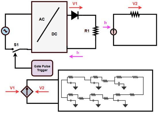
Figure 13.
Schematic representation of the surge current simulation setup.
6. Simulation Results
A transient thermal simulation was performed for both the PCT press-pack and insulated module diode to evaluate the temperature rise under various single half-sine peak current pulses, consistent with our previous work [45]. The simulation parameters are described in Table 3 and represented in Figure 14. The peak current amplitude was progressively increased until thermal runaway and subsequent device failure were observed.
Table 3.
Comparison of electrical and thermal characteristics: press pack vs. module.
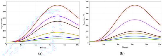
Figure 14.
Temperature under different surge peaks. (a) PCT press-pack diode (b) PCT insulated module diode.
The results indicate that while the increase in temperature remains moderate at lower currents for both devices, the insulated module diode experiences a significantly steeper temperature increase compared to the press-pack diode, especially at higher current levels. In particular, for the PCT press-pack diode, the junction temperature of 427 °C is reached at a peak current of approximately 30 kA. Beyond this, evaporation of metallization begins, resulting in cracking of the silicon chip at a junction temperature of around 597 °C with a peak current of 36.6 kA. In contrast, the failure of the insulated module diode occurs much earlier: the maximum junction temperature, i.e., 390 °C, is reached at only 26.8 kA of current, and silicon cracking is observed at approximately 30 kA.
These simulation results clearly demonstrate that the insulated diode module has inferior thermal performance compared to the press-pack diode. The single-sided current flow and presence of additional aluminium nitride support bars within the module package increase the thermal resistance of the module, resulting in inefficient heat dissipation, leading to reduced thermal capability. The corresponding data of current and temperature are presented in Figure 15, this time as a function of forward voltage rather than time. This alternative representation highlights the impact of temperature rise on the forward voltage drop and, consequently, the power dissipation of the device. As the junction temperature of the device increases, dynamic resistance also increases until device failure, leading to a higher forward voltage drop, as shown in Figure 16a,b. This, in turn, causes an increase in power dissipation (the product of forward current and voltage), thereby accelerating the temperature rise, leading to a typical mechanism of thermal runaway. Figure 16b corresponds to the diode module, clearly illustrating this effect: despite identical current pulse shapes and device ratings, the forward voltage of the module is noticeably higher compared to the press-pack diode. This increased forward voltage is directly linked to the elevated junction temperature. This behavior arises from differences in current distribution, double-sided in press-pack devices and single-sided in modules, as well as the additional presence of the AlN disc in modules, which substantially exacerbates the risk of thermal runaway.
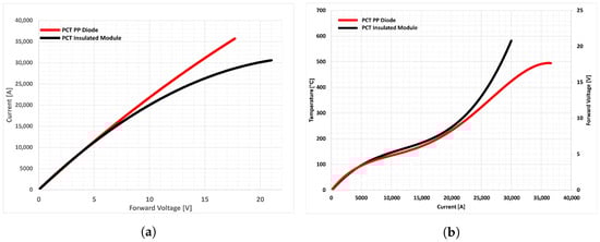
Figure 15.
(a) Surge trajectory, I-V curve. (b) V-T, I-T, and Tmax.
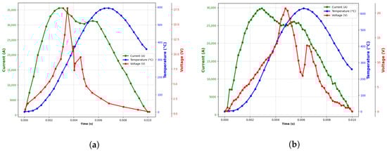
Figure 16.
Surge trajectory and I-V curve, V-T, I-T, and Tmax. (a) PCT press-pack diode. (b) PCT insulated module diode.
7. Device Failure Analysis
After subjecting the DUT to surge current stress and performing experimental tests, the failure mechanisms under two different scenarios were analyzed. In the case of press-pack diode, device failure, specifically micro-eroding, is primarily attributed to heating induced by the high surge current. As the surge current begins to increase, the concentration of carriers is also increased, which, in turn, increases the forward voltage drop of the device, and hence, the temperature is also increased. With further increases in surge peak, the concentration of carriers is increased, which affects the mobility of carriers, and hence, the slope of the I-V curve is slowly reduced. However, the change in the forward voltage drop of the diode remains linear until the 30 kA surge current is applied. When subjected to a 30 kA surge current, the forward voltage drop of the diode increases from 7.4 V to 13.8 V, and a minor change in the shape of the waveform is also noted. Moreover, a sharp falling time and the evaporation of metallization are noted on the silicon chip, as shown in Figure 17.
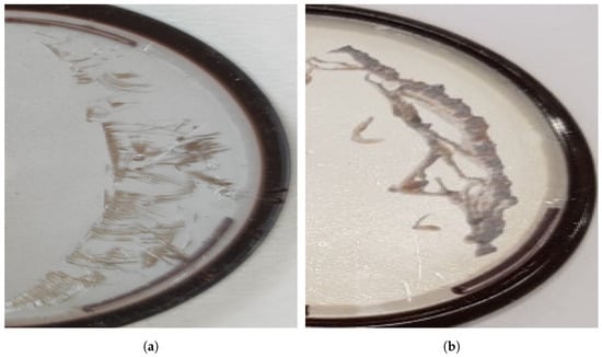
Figure 17.
Impact of evaporation of metal on silicon chip. (a) PCT press-pack diode. (b) PCT insulated module diode.
When subjected to a surge current of 36 kA, the voltage drop increases to approximately 17.7 V. Notably, the two peak voltages occur, i.e., at 3 ms and 5 ms, which is significantly earlier than the typical 4 ms peak observed under lower-stress conditions. This shift leads to a nonlinear relationship between forward voltage and junction temperature at high current levels. The reduction in voltage can be attributed to an increased internal resistance caused by non-uniform current conduction. This non-uniformity results from localized damage or failure within the device, i.e, evaporation of metallization and cracking of the silicon chip, which disrupts normal conduction and degrades overall device performance.
Upon unpacking the device, it is noted that molybdenum is damaged, as shown in Figure 18, and attached to the silicon chip; upon detaching, a rupture was observed at the outer edges of the molybdenum and silicon die, as shown in Figure 19. Consequently, device performance is degraded; however, the silicon chip remains partially functional, defining the limit of forward voltage and maximum junction temperature.
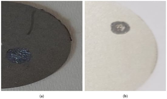
Figure 18.
Impact of surge on molybdenum. (a) PCT press-pack diode. (b) PCT insulated module diode.
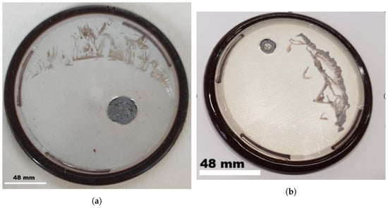
Figure 19.
Failure of the silicon chip. (a) PCT press-pack diode. (b) PCT insulated module diode.
At a peak amplitude of 36 kA, the high surge current leads to elevated temperatures, which is a typical phenomenon that can lead to failure. In addition to this, the chip, at an elevated temperature, exhibits a large strain and localized current at the beginning due to the increased concentration of carriers. As there is a barrier to the free movement of carriers, the temperature continues to rise, and there is a high possibility for the newly induced strain to give rise to chip breakage, as shown in Figure 20a. The higher defect densities in the chip with this kind of failure can originate from the thermal stress on the Si. As a result, the higher defect density contributes to a more concentrated heat distribution locally during surge current. This leads to more thermal stress, thereby reducing the mechanical strength of the chip. Thus, the breakage of the chip appears at the place where its defect states or residual stresses are high, as shown in Figure 20b. This result also indicates that surge current failure is closely connected to Si substrate quality. Moreover, it is noted that, although the insulated module diode exhibits significantly higher thermal resistance compared to the PCT press-pack diode, the thermal resistance over a 10 ms pulse shows minimal difference as shown in Figure 21. These thermal resistance values were experimentally extracted following the measurement procedure reported in our previous work [10]. As a result, a lower temperature rise difference and eventual device failure are observed in both cases. Notably, while the failure mode, which is characterized by metallization evaporation and chip rupture, is consistent across both devices, the extent of metal evaporation is, however, more severe in the insulated module diode compared to press-pack diodes. Moreover, the results also highlight that surge events of shorter duration can lead to increased forward voltage, resulting in defects in the silicon chip. In contrast, surge events of longer duration may result in higher thermal resistance, which is influenced by the device packaging technique. Although this study focuses on monolithic silicon diodes, the main conclusions are primarily driven by packaging architecture and thermal management mechanisms rather than silicon material properties alone. Therefore, the qualitative trends regarding junction temperature rise, surge robustness, and failure behavior are expected to remain applicable to SiC devices, albeit with different quantitative limits due to SiC’s higher thermal conductivity and allowable junction temperature. Moreover, for multi-chip module architectures, additional effects such as current sharing imbalance and increased interface-related thermal resistance may further influence surge performance. Nevertheless, the electro-thermal methodology and packaging-related insights presented in this work remain directly applicable.
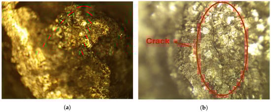
Figure 20.
Failure of silicon chip after surge test:(a) PCT press-pack diode. (b) PCT insulated module diode.
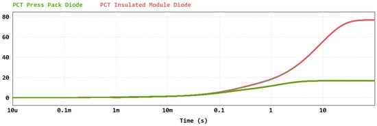
Figure 21.
Comparison of thermal impedance between PCT press-pack diode and PCT insulated module diode.
8. Conclusions and Future Directions
This paper presents a comparison between two high-power diode technologies, a press-pack ceramic housing diode and an insulated module diode based on pressure contact technology, with identical electrical ratings under high-surge-current conditions. A 10 ms half-sine surge generator was developed and implemented both experimentally and in simulations to represent realistic surge events. Moreover, experimental tests were performed to measure forward voltage and current waveforms. The measured waveforms of electrical parameters were then utilized in evaluating device performance, reliability, and robustness. Electro-thermal simulations were also carried out for estimation of junction temperature during surge events.
The results highlights the impact of packaging technology on the thermal performance and surge current robustness of the device. Furthermore, it is also noted that press-pack diode exhibiting superior thermal performance, lower junction temperatures, and improved surge handling capability. In contrast, the insulated module diode experienced a steeper temperature rise and an earlier onset of thermal limitations. Moreover, surge events with short-duration mainly cause defects in silicon through increased forward voltage, while long-duration surges results in increased thermal resistance due to packaging effects. Additionally, failure analysis also showed that a dominant degradation mechanism is associated with each packaging type. These results highlight a critical role of packaging technology in determining the electro-thermal behavior and reliability of high-power semiconductor devices and provides a practical guidance to select diode technologies in high-power applications.
Future work will focus on statistically evaluating surge failure thresholds across multiple devices to assess repeatability and variability. Moreover, the influence of interface-related parameters such as clamping force, surface condition, and aging on junction temperature and surge robustness will also be investigated. In addition, the proposed electro-thermal methodology will be extended to SiC devices and multi-chip module architectures to quantify material- and packaging-dependent effects on surge performance.
Author Contributions
Conceptualization: F.A., L.V. and M.M.; Methodology: F.A.; Modeling: F.A. and A.A.N.; Software: F.A.; Investigation: F.A. and G.A.; Formal Analysis: F.P.; Writing—Original Draft Preparation: F.A.; Writing—Review and Editing: L.V. and M.M.; Supervision: L.V. All authors have read and agreed to the published version of the manuscript.
Funding
This research was supported by Programma Regionale Fondo Sociale Europeo+ 2021–2027, Priorità 2—Istruzione e Formazione—ESO 4.6 (OS-f), Operazione “Scienze e tecnologie per l’ingegneria elettrica e i sistemi complessi per la mobilità”, carried out in collaboration with Poseico Power Electronics S.p.A., Genoa, Italy. The funding does not cover the cost of this publication.
Data Availability Statement
Data are available and may be provided by the authors upon request.
Acknowledgments
The authors would like to express their sincere gratitude to Marco Portesine of Poseico Power Electronics S.p.A. for his continuous guidance, insightful feedback, and valuable support throughout the preparation and refinement of this work.
Conflicts of Interest
The authors Fawad Ahmad, Federico Portesine and Giulio Anyanwu are employed by the company Poseico Power Electronics S.p.A. The remaining authors declare that the research was conducted in the absence of any commercial or financial relationships that could be construed as potential conflicts of interest.
References
- Marchesoni, M.; Passalacqua, M.; Vaccaro, L.; Carpita, M.; Gavin, S.; Kissling, S. Capacitor voltage ripple minimization in voltage source converter for HVDC applications. In Proceedings of the 2019 AEIT HVDC International Conference (AEIT HVDC), Florence, Italy, 9–10 May 2019; IEEE: Piscataway, NJ, USA, 2019; pp. 1–6. [Google Scholar]
- Araneda, J.; Yuyuniz Gálvez, C.; Morán, L.; Vaccaro, L. Reactive Power Compensation System for the Chilean HVDC Transmission Line. In Proceedings of the 2025 AEIT HVDC International Conference (AEIT HVDC), Genova, Italy, 29–30 May 2025; IEEE: Piscataway, NJ, USA, 2025; pp. 1–6. [Google Scholar]
- Benevieri, A.; Carbone, L.; Cosso, S.; Kumar, K.; Marchesoni, M.; Passalacqua, M.; Vaccaro, L. Series architecture on hybrid electric vehicles: A review. Energies 2021, 14, 7672. [Google Scholar] [CrossRef]
- Nkembi, A.A.; Santoro, D.; Ahmad, F.; Kortabarria, I.; Cova, P.; Sacchi, E.; Delmonte, N. Novel Droop-Based Techniques for Dynamic Performance Improvement in a Linear Active Disturbance Rejection Controlled-Dual Active Bridge for Fast Battery Charging of Electric Vehicles. Energies 2024, 17, 5171. [Google Scholar] [CrossRef]
- Benevieri, A.; Cosso, S.; Formentini, A.; Marchesoni, M.; Passalacqua, M.; Vaccaro, L. Advances and Perspectives in Multilevel Converters: A Comprehensive Review. Electronics 2024, 13, 4736. [Google Scholar] [CrossRef]
- Choi, U.M.; Blaabjerg, F.; Jørgensen, S. Study on effect of junction temperature swing duration on lifetime of transfer molded power IGBT modules. IEEE Trans. Power Electron. 2017, 32, 6434–6443. [Google Scholar] [CrossRef]
- Wu, X.; Liu, W. An engineering roadmap for the thermoelectric interface materials. J. Mater. 2024, 10, 748–750. [Google Scholar] [CrossRef]
- Oh, H.; Han, B.; McCluskey, P.; Han, C.; Youn, B.D. Physics-of-failure, condition monitoring, and prognostics of insulated gate bipolar transistor modules: A review. IEEE Trans. Power Electron. 2014, 30, 2413–2426. [Google Scholar] [CrossRef]
- Ge, X.; Chen, K.; Wang, H.; Xu, Z.; Fu, Z. Failure Mechanism Investigations of Bond Wires Lifting-Off and Die-Attach Solder Aging Considering the Thermal Coupling Effects. IEEE Trans. Power Electron. 2025, 40, 2042–2056. [Google Scholar] [CrossRef]
- Ahmad, F.; Portesine, F.; Ashero, M.; Marchesoni, M.; Vaccaro, L. Transient Thermal Impedance Characterization of New High Power Press Pack Diodes. In Proceedings of the 2024 International Symposium on Power Electronics, Electrical Drives, Automation and Motion (SPEEDAM), Napoli, Italy, 19–21 June 2024; IEEE: Piscataway, NJ, USA, 2024; pp. 81–86. [Google Scholar]
- Rodrigues, R.; Zhang, Y.; Jiang, T.; Aeloiza, E.; Cairoli, P. Surge current capability of SiC MOSFETs in AC distribution systems. In Proceedings of the 2018 IEEE 6th Workshop on Wide Bandgap Power Devices and Applications (WiPDA), Atlanta, GA, USA, 31 October–2 November 2018; pp. 331–337. [Google Scholar] [CrossRef]
- Palanisamy, S.; Yoganath, G.V.; Zeng, G.; Lutz, J.; Kowalsky, J.; Basler, T. Temperature determination of SiC MPS diodes during surge current event with measurement and simulation. In Proceedings of the 2019 21st European Conference on Power Electronics and Applications (EPE’19 ECCE Europe), Genova, Italy, 2–5 September 2019; IEEE: Piscataway, NJ, USA, 2019; p. P-1. [Google Scholar]
- Nehmer, D.; Ringelmann, T.; Bakran, M.M. Modelling and Evalaution of the Bidirectional Surge Current Robustness of Si(-IGBT and -Diode), SiC(-MOSFETs and -JFET) and GaN(-HEMTs) Devices. Energies 2024, 17, 4362. [Google Scholar] [CrossRef]
- Soeiro, T.B.; Mengotti, E.; Bianda, E.; Ortiz, G. Performance Evaluation of the Body-Diode of SiC Mosfets under Repetitive Surge Current Operation. In Proceedings of the IECON 2019—45th Annual Conference of the IEEE Industrial Electronics Society, Lisbon, Portugal, 14–17 October 2019; Volume 1, pp. 5154–5159. [Google Scholar] [CrossRef]
- Wu, J.; Ren, N.; Sheng, K. Electrothermal Coupling Model With Distributed Heat Sources for Junction Temperature Calculation During Surges. IEEE Trans. Power Electron. 2022, 37, 11887–11895. [Google Scholar] [CrossRef]
- Abuelnaga, A.; Narimani, M.; Bahman, A.S. A review on IGBT module failure modes and lifetime testing. IEEE Access 2021, 9, 9643–9663. [Google Scholar] [CrossRef]
- Wu, R.; Blaabjerg, F.; Wang, H.; Liserre, M. Overview of catastrophic failures of freewheeling diodes in power electronic circuits. Microelectron. Reliab. 2013, 53, 1788–1792. [Google Scholar] [CrossRef]
- Zhang, J.; Deng, E.; Zhao, Z.; Li, J.; Huang, Y. Simulation on fatigue failure of single IGBT chip module of press-pack IGBTs. Trans. China Electrotech. Soc. 2018, 33, 4277–4285. [Google Scholar]
- Poller, T.; Basler, T.; Hernes, M.; D’Arco, S.; Lutz, J. Mechanical analysis of press-pack IGBTs. Microelectron. Reliab. 2012, 52, 2397–2402. [Google Scholar] [CrossRef]
- Loh, W.S.; Corfield, M.; Lu, H.; Hogg, S.; Tilford, T.; Johnson, C.M. Wire bond reliability for power electronic modules-effect of bonding temperature. In Proceedings of the 2007 International Conference on Thermal, Mechanical and Multi-Physics Simulation Experiments in Microelectronics and Micro-Systems, EuroSime 2007, London, UK, 16–18 April 2007; IEEE: Piscataway, NJ, USA, 2007; pp. 1–6. [Google Scholar]
- Delepaut, C.; Siconolfi, S.; Mourra, O.; Tonicello, F. MOSFET gate open failure analysis in power electronics. In Proceedings of the 2013 Twenty-Eighth Annual IEEE Applied Power Electronics Conference and Exposition (APEC), Long Beach, CA, USA, 17–21 March 2013; IEEE: Piscataway, NJ, USA, 2013; pp. 189–196. [Google Scholar]
- Li, T.; Wang, Y.; Zhang, Y.; Fan, J.; Li, X.; Qi, L.; Cui, X. Impacts of the pressure distribution on dynamic avalanche in single press-pack IGBT chip. IEEE Trans. Power Electron. 2024, 39, 8187–8201. [Google Scholar] [CrossRef]
- Jian, Y.; Peng, S.; Chen, Z.; He, Z.; He, L.; Lv, X. Influence of different vibration directions on the solder layer fatigue in IGBT modules. Microelectron. Reliab. 2024, 162, 115526. [Google Scholar] [CrossRef]
- Xiao, K.; Wang, Z.; Yan, X.; Li, W.; Liu, Y.; Liu, P. Temperature Distribution and Mechanical Stress Analysis of Press-Pack IGBT Single Chip Under Different Operations. In Proceedings of the Frontier Academic Forum of Electrical Engineering; Springer: Cham, Switzerland, 2025; pp. 789–796. [Google Scholar]
- Li, H.; Yao, R.; Lai, W.; Ren, H.; Li, J. Modeling and analysis on overall fatigue failure evolution of press-pack IGBT device. IEEE Trans. Electron Devices 2019, 66, 1435–1443. [Google Scholar] [CrossRef]
- Fu, H.; Li, Y.; Li, Q.; Tu, C.; Xiao, B.; Xiao, F.; Liu, P.; Gao, B.; Lu, J. Failure mechanism analysis of bond wire of high power IGBT under different load current. In Proceedings of the 2022 IEEE 5th International Electrical and Energy Conference (CIEEC), Nanjing, China, 27–29 May 2022; IEEE: Piscataway, NJ, USA, 2022; pp. 798–803. [Google Scholar]
- Zhang, Y.; Zhan, C.; Zhu, L.; Dou, L.; Wang, W.; Ji, S.; Jin, Y.; Liu, X. Condition deterioration mechanisms of high voltage press-pack IGBT under power cycling test. In Proceedings of the 2022 IEEE International Conference on High Voltage Engineering and Applications (ICHVE), Chongqing, China, 25–29 September 2022; IEEE: Piscataway, NJ, USA, 2022; pp. 1–4. [Google Scholar]
- Tinschert, L.; Årdal, A.R.; Poller, T.; Bohlländer, M.; Hernes, M.; Lutz, J. Possible failure modes in Press-Pack IGBTs. Microelectron. Reliab. 2015, 55, 903–911. [Google Scholar] [CrossRef]
- Liu, R.; Li, H.; Yao, R.; Wang, X.; Tan, H.; Lai, W.; Yu, Y.; Zhu, Z.; Zhou, B. Research on Long-term Reliability of Silver Sintered Press-Pack IGBT Modules. Power Electron. Devices Components 2022, 3, 100012. [Google Scholar] [CrossRef]
- Peng, Y.; Shen, Y.; Wang, H. A converter-level on-state voltage measurement method for power semiconductor devices. IEEE Trans. Power Electron. 2020, 36, 1220–1224. [Google Scholar] [CrossRef]
- Peng, Y.; Zhao, S.; Wang, H. A digital twin based estimation method for health indicators of DC–DC converters. IEEE Trans. Power Electron. 2020, 36, 2105–2118. [Google Scholar] [CrossRef]
- Dupont, L.; Avenas, Y.; Jeannin, P.O. Comparison of junction temperature evaluations in a power IGBT module using an IR camera and three thermosensitive electrical parameters. IEEE Trans. Ind. Appl. 2013, 49, 1599–1608. [Google Scholar] [CrossRef]
- Luo, H.; Li, W.; Iannuzzo, F.; He, X.; Blaabjerg, F. Enabling junction temperature estimation via collector-side thermo-sensitive electrical parameters through emitter stray inductance in high-power IGBT modules. IEEE Trans. Ind. Electron. 2017, 65, 4724–4738. [Google Scholar] [CrossRef]
- Wang, Z.; Tian, B.; Qiao, W.; Qu, L. Real-time aging monitoring for IGBT modules using case temperature. IEEE Trans. Ind. Electron. 2015, 63, 1168–1178. [Google Scholar] [CrossRef]
- Scheuermann, U.; Schmidt, R. Impact of solder fatigue on module lifetime in power cycling tests. In Proceedings of the 2011 14th European Conference on Power Electronics and Applications, Birmingham, UK, 30 August–1 September 2011; IEEE: Piscataway, NJ, USA, 2011; pp. 1–10. [Google Scholar]
- Choi, U.M.; Blaabjerg, F.; Jørgensen, S.; Munk-Nielsen, S.; Rannestad, B. Reliability improvement of power converters by means of condition monitoring of IGBT modules. IEEE Trans. Power Electron. 2016, 32, 7990–7997. [Google Scholar] [CrossRef]
- Smet, V.; Forest, F.; Huselstein, J.J.; Rashed, A.; Richardeau, F. Evaluation of V_ce Monitoring as a Real-Time Method to Estimate Aging of Bond Wire-IGBT Modules Stressed by Power Cycling. IEEE Trans. Ind. Electron. 2012, 60, 2760–2770. [Google Scholar] [CrossRef]
- Huang, H.; Mawby, P.A. A lifetime estimation technique for voltage source inverters. IEEE Trans. Power Electron. 2012, 28, 4113–4119. [Google Scholar] [CrossRef]
- Gonzalez-Hernando, F.; San-Sebastian, J.; Garcia-Bediaga, A.; Arias, M.; Iannuzzo, F.; Blaabjerg, F. Wear-out condition monitoring of IGBT and MOSFET power modules in inverter operation. IEEE Trans. Ind. Appl. 2019, 55, 6184–6192. [Google Scholar] [CrossRef]
- Sasaki, K.; Iwasa, N.; Kurosu, T.; Saito, K.; Koike, Y.; Kamita, Y.; Toyoda, Y. Thermal and structural simulation techniques for estimating fatigue life of an IGBT module. In Proceedings of the 2008 20th International Symposium on Power Semiconductor Devices and IC’s, Orlando, FL, USA, 18–22 May 2008; IEEE: Piscataway, NJ, USA, 2008; pp. 181–184. [Google Scholar]
- Ciappa, M. Selected failure mechanisms of modern power modules. Microelectron. Reliab. 2002, 42, 653–667. [Google Scholar] [CrossRef]
- Yang, L.; Agyakwa, P.A.; Johnson, C.M. Physics-of-failure lifetime prediction models for wire bond interconnects in power electronic modules. IEEE Trans. Device Mater. Reliab. 2012, 13, 9–17. [Google Scholar] [CrossRef]
- IEC-60747-2; Semiconductor Devices—Part 2: Discrete Devices—Rectifier Diodes. International Electrotechnical Commission (IEC): Geneva, Switzerland, 2016.
- Asadi, F.; Eguchi, K. Power Electronics Circuit Analysis with PSIM®; Walter de Gruyter GmbH & Co KG: Berlin, Germany, 2021. [Google Scholar]
- Ahmad, F.; Vaccaro, L.; Nkembi, A.A.; Marchesoni, M.; Portesine, F. Surge Current Analysis of High-Power Press Pack Diodes: Junction Temperature and Forward-Voltage Modeling. Electronics 2025, 14, 4899. [Google Scholar] [CrossRef]
Disclaimer/Publisher’s Note: The statements, opinions and data contained in all publications are solely those of the individual author(s) and contributor(s) and not of MDPI and/or the editor(s). MDPI and/or the editor(s) disclaim responsibility for any injury to people or property resulting from any ideas, methods, instructions or products referred to in the content. |
© 2025 by the authors. Licensee MDPI, Basel, Switzerland. This article is an open access article distributed under the terms and conditions of the Creative Commons Attribution (CC BY) license.