Abstract
In this paper, the electromagnetic pulse (EMP) sensitivity of power modules of field-programmable gate arrays (FPGAs) is studied experimentally. Two FPGAs with different manufacturing processes are adopted. The pulse current injection (PCI) is, respectively, conducted on four independent power lines of FPGA test boards, and a specialized test program is designed to explore the influences of resource types and frequencies. The experimental results indicate that different power modules have significantly distinct failure characteristics and thresholds. For each power module, high-frequency (HF) signals generally exhibit greater sensitivity than constant signals in most cases, with frequency being a critical influencing factor. In addition, the EMP sensitivity of the VCCAUX can also be affected by resource types and location constraints. All power modules exhibit different sensitivities to PCIs of different polarities, with the negative injection showing more complex failure characteristics. The manufacturing processes of FPGAs have a slight impact on the EMP sensitivity of their power modules, which is only reflected on the VCCINT. In the case of enabled programmable read-only memory (PROM), an FPGA automatic reconfiguration process has been observed during the PCI experiment for the first time. Moreover, high-value capacitors on the power distribution network (PDN) provide effective filtering by reducing the amplitude and slowing down the edge of the pulsed current.
1. Introduction
Field-programmable gate arrays (FPGAs) have often been used for digital signal processing and system function expansion thanks to their high programmability, excellent performance, and commendable stability. However, these widespread applications mean that they will be exposed to complex environments, subject to various types of radiations [1,2,3,4,5,6]. Electromagnetic pulse (EMP), as an important radiation source, is characterized by the broad frequency band energy distribution, elevated peak field strength, and extensive regional impact [7,8,9,10]. It can couple with various conductive paths, generating high current or voltage pulses that can cause FPGAs to have transient failures or even permanent damage.
On the one hand, previous experimental studies on EMP sensitivity have primarily focused on smaller-scale electronic devices [11,12,13], with relatively simple experimental setups and test systems. In comparison, for FPGAs, as highly integrated, functionally complex, and high-speed computing electronic systems, their experimental study on the EMP sensitivity needs to consider multiple variables and ensure the precise monitoring of critical points in a complex environment. On the other hand, most existing studies on FPGAs focus on electromagnetic immunity (EMI) testing at different frequencies, while research specifically on EMP sensitivity remains limited. Additionally, most of these existing studies on FPGAs primarily examine local resources (IOs, PLLs, and DLLs, etc.) [14,15,16], with relatively little attention given to the EMP sensitivity of power modules [17].
However, as FPGAs advance to higher speeds and greater functional densities, the requirements for power integrity (PI) are also increasing [18,19,20]. Higher operating frequencies and more transistor switches and complex power distribution networks (PDNs) can all lead to significant synchronous switching noise (SSN) and parasitic effects, combined with lower supply voltages and higher operating currents. These factors will reduce the voltage noise tolerance. More importantly, the PI is critical in maintaining global signal stability, especially in extreme electromagnetic environments. Power module failures can degrade global signal quality and impact the overall performance of FPGAs. In addition, FPGAs usually have several power modules, which may have different output failure characteristics, influencing factors and sensitive circuits. In contrast, the impact on signal integrity (SI) tends to remain local. This distinction reflects that assessing the sensitivity for power modules of FPGAs appears to be more important than local signal modules in the EMP environment, which is also an important difference between this study and previous research.
Experimental methods for evaluating the EMP sensitivity of integrated circuits (ICs) include radiation and pulsed current injection (PCI). Radiation means exposing the device to the EMP field and assessing its overall response, while this makes specific sensitivity analysis more difficult [21,22]. In contrast, PCI involves injecting a pulsed current into a specific module of the device, allowing for the precise control of pulse parameters and facilitating the study of local EMP sensitivity under varying conditions [23,24]. Moreover, PCI offers greater efficiency and a lower cost compared to radiation.
In this work, the PCI method is adopted to investigate the EMP sensitivity of different power modules in two typical FPGAs. The findings complement the research field on the EMP sensitivity of FPGAs by providing more detailed experimental phenomena and data under different studied variables, as well as feasible references and a theoretical analysis basis for future experimental research on EMP sensitivity for different types and processes of FPGAs.
2. Experimental Methods
2.1. Device Under Test (DUT)
The JXCV5SX95T and XC5VSX95T FPGAs are examined in the PCI experiment, and are manufactured by two different companies using different processes. The XC5VSX95T, a 60 nm device, belongs to the Xilinx Virtex-5 family and is developed by Xilinx, based in San Jose, California, USA. The JXCV5SX95T is developed by China Electronics Technology Group Corporation (CETC) in Beijing, China, and manufactured via a 45 nm process. More detailed information can be obtained in their manuals [25]. These two FPGAs with typical structures are widely applied in high-performance digital processing and communication in practice. Importantly, they are functionally pin-to-pin interchangeable, allowing them to be placed on the same test board. This eliminates the influence of the DUT’s peripheral circuits, ensuring a more accurate sensitivity analysis.
The test board of DUT (JXCV5SX95T and XC5VSX95T) is shown in Figure 1a. It has four independent power distribution networks (PDNs) with voltages of 1.1, 1.8, 2.5, and 3.3 V, and all of them are connected to external power lines through four power ports. In addition, there is an FPGA chip, a configuration chip, the Joint Test Action Group (JTAG) interface, SubMiniature version A (SMA) ports, FPGA Mezzanine Card (FMC) interfaces, and some passive components on the test board. The input signal is provided by connecting the SMA port to the signal generator. The output signals are transferred through the FMC interface to the adapter board (Figure 1b), which is connected to oscilloscopes through the SMA ports.
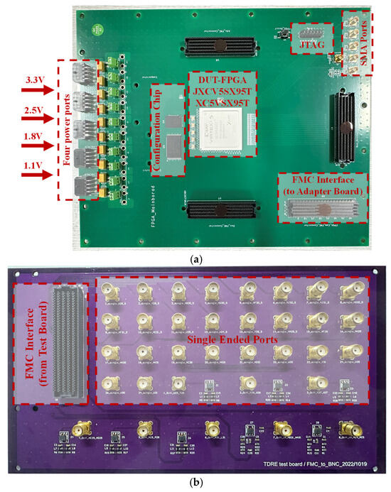
Figure 1.
Photo of the tested DUT and its output adapter. (a) Photo of the DUT (JXCV5SX95T or XC5VSX95T) test board. (b) Photo of the adapter board.
2.2. Test Program
Previous studies have found that operation states of clock resources and Configurable Logic Blocks (CLBs) of FPGAs are susceptible to various radiation effects [26,27]; therefore, it can be suspected that their power modules are also sensitive to the EMP. Moreover, as a critical component in digital processing and connection, the FPGA is often combined with other functional chips to form a complete system, so that its output faults can propagate between different chips, potentially affecting the overall function of the system.
Therefore, the designed test program consists of two parts. In the first part, the influences of types and frequencies of clock resources are investigated. As shown in Figure 2, the clock resources of FPGAs mainly include Delay-Locked Loops (DLLs), Phase-Locked Loops (PLLs), and General Clock Buffers (GCBs). The 50MHz input sys_clk is configured as 7 outputs (output 1 to 7). In addition, considering the influence of IO ports, the input sys_clk is directly output without utilizing any resources (output8).
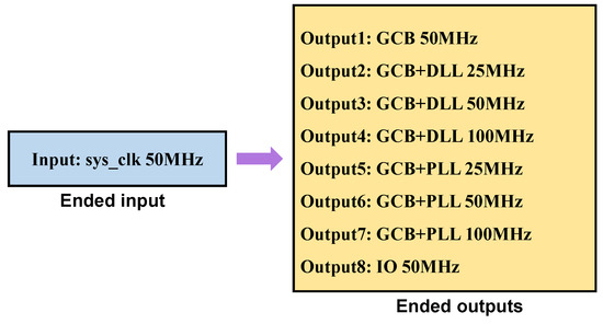
Figure 2.
The diagram of test program for clock resources, considering influences of types, frequencies, and IO ports.
The second part focuses on system-level communication between the FPGA and other modules. With the FPGA as the core, common modules, such as an ADC, DAC, or bus driver are selected, and their states depend on the configuration of the FPGA. The whole system is consistent with the SiP SZ0501 and its prototype board in transient γ irradiation experiments [28,29]. Figure 3 is a diagram of program configuration, including the following three aspects:
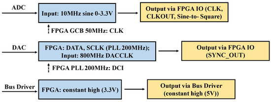
Figure 3.
The diagram of test program for communication between the FPGA and other modules (ADC, DAC, and bus driver).
2.3. Pulsed Current Generation, Injection, and Detection
Figure 4a is a schematic diagram of the physical configuration of the PCI experiment. A typical 20/500 ns double-exponential pulsed current generator is adopted [24], whose output is connected to an inductive coupled injection ring. The target power line of the test board is passed through the central space of the injection ring, allowing for the indirect injection of 20/500 ns double-exponential pulsed currents (Figure 4b) with adjustable amplitude and polarity into the power line. Based on the principle of electromagnetic induction, when the pulsed current flows through the injection loop, it generates a varying magnetic field in the surrounding space. This magnetic field induces a coupling current in the power line through electromagnetic induction. Therefore, this injection method does not need to establish direct electrical contact with the DUT, but only through magnetic field coupling to achieve energy transfer, effectively avoiding the interference of physical contact in the circuit operating state [30]. Furthermore, the electrical isolation between the injection loop and the power line ensures that the normal operating conditions of the DUT remain unaffected, while also enhancing the safety and reliability of the experiment. Additionally, the output of the current detection loop is connected to oscilloscopes to capture the waveform of the pulsed current injected into the power line. During the injection, all oscilloscopes are synchronously triggered by the output of the current detection loop to record the outputs of the system.
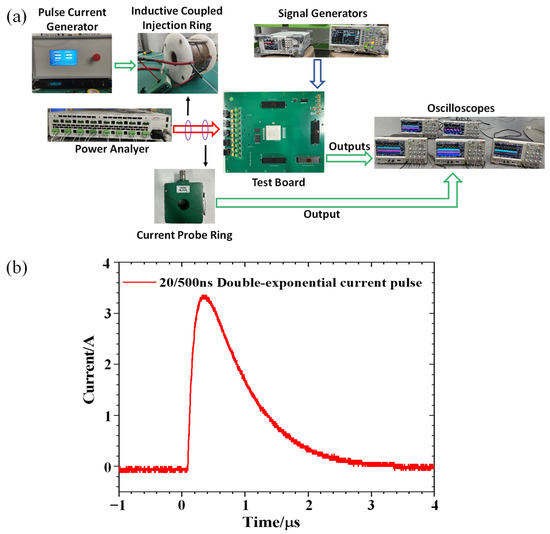
Figure 4.
The schematic of physical configuration of the PCI experiment (a) and the waveform of 20/500 ns double-exponential pulsed current (b).
2.4. Flow of Experiments
After powering on the JXCV5SX95T test board, the test program would be automatically loaded via the configuration chip, and the system would be automatically configured. The loading voltage step of the pulse generator is set to 200 V. As the injection amplitude increases, outputs of the system and the pulsed current waveform are recorded using oscilloscopes. Positive and negative PCIs are conducted on each power line of the test board, respectively. Then, the JXCV5SX95T test board is replaced with XCV5SX95T, and the above process is repeated.
For the two FPGAs, three samples were selected for testing, respectively. At each amplitude, injection was repeated three times, and the pulsed current amplitude was recorded. The average value was taken as the final experimental data, effectively reducing random errors and improving data reliability and accuracy.
3. Experimental Results and Analysis
3.1. Positive PCI into Power Lines of the JXCV5SX95T Test Board
The positive PCI is conducted, respectively, on four power lines of the JXCV5SX95T test board, which supplies different power modules. The experimental results demonstrate that the power modules of the JXCV5SX95T are sensitive to positive PCI. There are output faults during injection into the 1.8 V, 3.3 V, and 2.5 V power lines, with no fault in the 1.1 V.
3.1.1. Injection into 1.8 V Power Line
The 1.8V power line supplies the HF output ports of the JXCV5SX95T. The experimental results indicate that the positive PCI can cause disturbances in all HF outputs with the same trend. The frequency is also a main factor in the degree of disturbance, as shown in Figure 5.
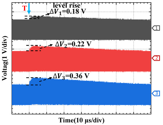
Figure 5.
More significant level rise in FPGA IO 50 MHz as the amplitude of positive injection into the 1.8 V power line increases. Injection amplitudes of 1, 2, and 3 are 12.7 A, 19 A, and 25.5 A, respectively.
Figure 6 shows the output disturbances of PLLs at different configuration frequencies under a 12.7 A PCI. It can be found that the higher the frequency, the more serious the rise in output level. A higher frequency means faster logic transitions at the output port, leading to more significant synchronous switching noise (SSN) on the 1.8 V PDN [31]. The increased SSN can affect the PI, making the output port more sensitive to PCI.
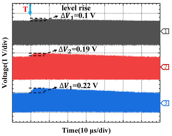
Figure 6.
At an injection amplitude of 12.7 A, the higher the frequency of GCB + PLL, the more severe level rise for the FPGA. Signals 1, 2, and 3 correspond to 25 MHz, 50 MHz, and 100 MHz, respectively.
3.1.2. Injection into 3.3 V Power Line
The 3.3 V power line supplies the input sys_clk port and the output constant high (3.3 V) port of the JXCV5SX95T. Table 1 briefly summarizes the failure characteristics and thresholds during the positive PCI. Faults are only generated in HF outputs. They manifest in two distinct failure stages: (1) Partial HF outputs (FPGA IO, FPGA GCB, and ADC_CLK) have disturbances simultaneously and (2) all HF outputs, except for DAC_SYNC_OUT, experience a period of loss simultaneously. The DAC_SYNC_OUT is derived from a differential input port supplied by 2.5 V, and is output through a single-ended port supplied by 1.8 V. Therefore, it can remain stable during PCI into the 3.3 V power line.

Table 1.
Results of the positive PCI into 3.3V power line of the JXCV5S95T test board.
According to the test program, all HF outputs except DAC_SYNC_OUT require a stable sys_clk input to the FPGA. However, the positive PCI into the 3.3 V power line can disrupt the operating state of the sys_clk port, interfering with the transmission of sys_clk to the FPGA. This interference can be monitored via the FPGA IO, which is configured as direct output without utilizing any resources of the JXCV5SX95T.
Figure 7 corresponds to the first failure stage. The FPGA IO, FPGA GCB, and ADC_CLK have basically the same disturbance after injection (T). In addition, both the FPGA GCB and ADC_CLK utilize the same type of resources (GCB). This indicates that the low-amplitude positive PCI has a slight interference upon sys_clk entering the JXCV5SX95T, resulting in its dropping. And this drop can only affect the operating state of the GCB, while other types of resources in the JXCV5SX95T remain normal.
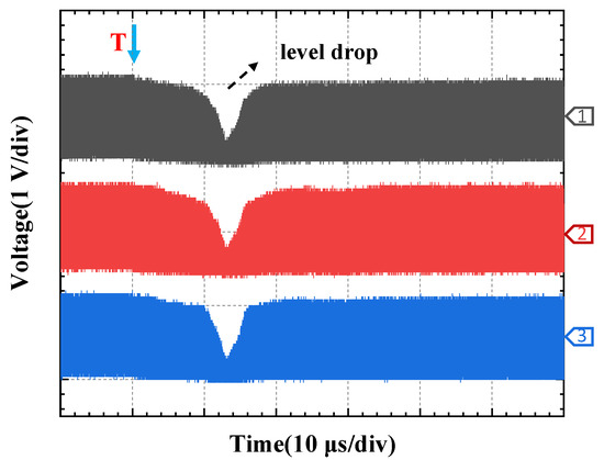
Figure 7.
Level drops of FPGA IO 50 MHz (signal 1), FPGA GCB 50 MHz (signal 2), and ADC_CLK 50 MHz (signal 3) for a 72.9 A PCI into the 3.3 V power line of the JXCV5SX95T test board.
Figure 8 corresponds to the second failure stage. All HF outputs except DAC_DYNC_OUT experience a period of loss at the same time. FPGA IO, FPGA GCB, and ADC_CLK still have disturbances before and after the loss. The waveform of FPGA IO indicates that as the injection amplitude increases, significant interference occurs when sys_clk enters the JXCV5SX95T, leading to a period of loss in the sys_clk. During this period, all configured clock resources (GCB, PLL, and DLL) inside the JXCV5SX95T have no input, causing their HF outputs to be lost as well. The duration of this loss is independent of the configured frequency. Moreover, when the sampling clock (ADC_CLK) provided by the FPGA to ADC is lost, the state of ADC is also affected, which eventually results in the loss of further data comparison in the FPGA (ADC_CLKOUT and ADC sine-to-square).
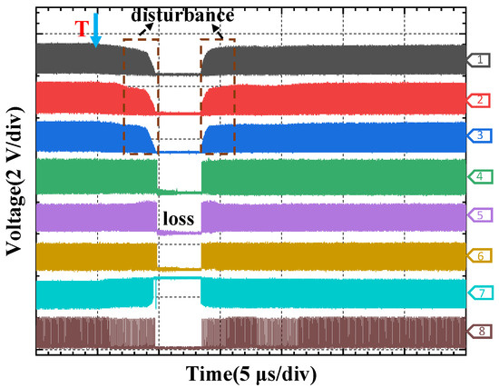
Figure 8.
When the 75.3 A PCI into the 3.3 V power line of JXCV5SX95T test board takes place, there are disturbances in FPGA IO (signal 1), FPGA GCB (signal 2), and ADC_CLK (signal 3), and losses in all HF outputs except DAC_SYNC_OUT. FPGA GCB + PLL and FPGA GCB + DLL, with the same frequency, have the same failure characteristics. Signals 4, 5, 6, 7, and 8 correspond to FPGA GCB + DLL 25 MHz, FPGA GCB + DLL 50 MHz, FPGA GCB + DLL 100 MHz, ADC_CLKOUT 50 MHz, and ADC sine-to-square 10 MHz, respectively.
3.1.3. Injection into 2.5 V Power Line
The 2.5 V power line primarily supplies the auxiliary voltage (VCCAUX) of the JXCV5SX95T. The experimental results show that the HF outputs of only DLLs have faults during positive PCI; their failure thresholds and characteristics are shown in Table 2 and Figure 9, respectively. It can be found that DLLs at different frequencies have different failure thresholds. The failure characteristics of the 25 MHz DLL are obviously different from others, which presents longer loss after injection (T).
Table 2.
Failure thresholds of HF outputs for the positive PCI into 2.5 V power line of the JXCV5SX95T test board.
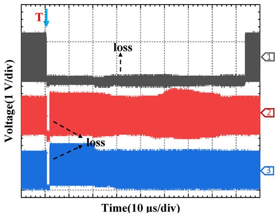
Figure 9.
Different loss waveforms of DLLs with different frequencies for a 64.9 A PCI into 2.5 V power line of JXCV5SX95T test board. Signals 1, 2, and 3 correspond to 25 MHz, 50 MHz, and 100 MHz, respectively.
3.2. The Comparison of PCIs of Different Polarities
FPGAs may be subjected to EMP radiation from different directions, which can generate pulsed current of different polarities into their power modules [32]. Therefore, the negative PCI is also conducted, respectively, to four power lines of the JXCV5SX95T test board. The experimental results indicate that power modules of the JXCV5SX95T exhibit different sensitivities to PCIs of different polarities.
3.2.1. Injection into 1.8 V Power Line
The negative PCI into the 1.8 V power line can also cause all HF outputs to have a disturbance with the same trend, but the disturbance direction is opposite to the positive PCI. Figure 10 compares the outputs of FPGA IO for PCIs with different polarities. The fast-falling edge can pull the voltage down at 1.8V PDN, making all HF output ports of the JXCV5SX95T operate in an under-voltage state [33]. This ultimately leads to the level drop of FPGA IO.
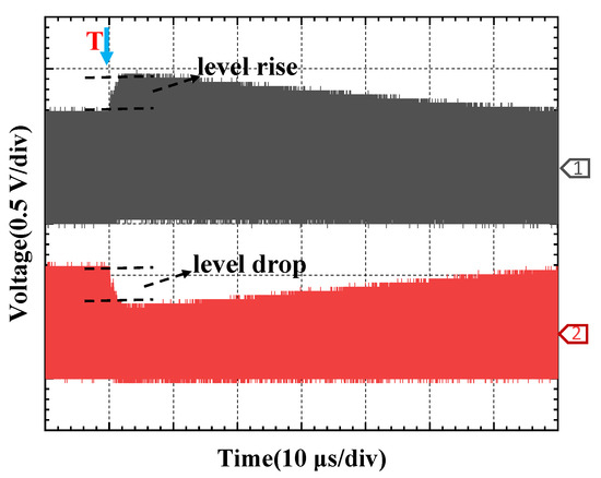
Figure 10.
Outputs of FPGA IO for PCIs with different polarities. The positive injection induces level rise, the negative injection induces level drop. Signals 1 and 2 correspond to positive and negative injection, respectively.
3.2.2. Injection into 3.3 V Power Line
Differently from positive PCI, during the negative PCI into the 3.3 V power line, HF outputs and the constant output of the system all exhibit faults. In addition, the auto-reconfiguration process of the FPGA is found. Table 3 summarizes the failure thresholds.
Table 3.
Failure characteristics and thresholds of the negative PCI into 3.3 V power line of JXCV5SX95T test board.
From Table 3, it can be seen that as the injection amplitude of the negative PCI increases, the HF outputs have the same failure stages but different failure thresholds compared to the positive PCI. Figure 11 compares the waveforms of HF outputs in two failure stages for different polarity injections via FPGA IO. Disturbance or loss after negative injection (T) is obviously slower than that after positive injection, and the same is true for the other HF outputs.
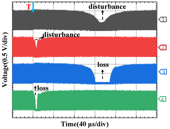
Figure 11.
Failure waveforms of FPGA IO 50 MHz in two failure stages for injections of different polarities. Signal 1 corresponds to first stage for negative PCI. Signal 2 corresponds to first stage for positive PCI. Signal 3 corresponds to second stage for negative PCI. Signal 4 corresponds to second stage for positive PCI.
The constant high output (5 V) of bus driver does not exhibit faults during the positive PCI. The −97.2 A PCI into the 3.3 V power line can cause it to have a temporary logic upset. As the injection amplitude increases, the duration of upset will also increase, as illustrated in Figure 12. The constant high output (5 V) of bus driver is derived from the constant high output (3.3 V) of the JXCV5SX95T, whose port is supplied by the 3.3 V power line. Consequently, similarly to the disturbance observed in HF outputs during the negative PCI into the 1.8 V power line, the negative PCI into the 3.3 V power line can also cause the same feature level drop at the constant high output (3.3 V). When this drop is smaller than the high-level threshold of the bus driver input port, a logic upset appears in the bus driver output (from ‘5 V’ to ‘0 V’). This condition persists until the constant high output (3.3 V) recovers to a recognizable level, at which point the constant high output (5 V) also returns to normal. Furthermore, a larger injection amplitude can induce a more serious level drop on the constant high output (3.3 V), which ultimately leads to a longer upset on the constant high output (5 V). Conversely, the positive PCI causes the level of the constant high output (3.3 V) to rise, which is still recognized via the high level of the bus driver, thus preventing any output faults from occurring.
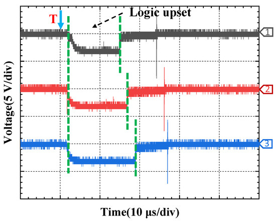
Figure 12.
Longer logic upsets with constant high output (5 V) as the amplitude of the negative injection into the 3.3 V power line of JXCV5SX95T test board increases. Injection amplitudes of signals 1, 2, and 3 are −97.2 A, −105 A, and −109 A, respectively.
When the injection amplitude reaches −126 A, the JXCV5SX95T loses all configuration functions, resulting in the loss of all system outputs. However, in the case of the enabled PROM, the JXCV5SX95T fully recovers again after a few seconds and the system also returns to normal. This is the first time that the auto-reconfiguration process has been found in an PCI experiment on FPGAs. This phenomenon has been observed in previous experimental studies about the transient dose rate effect (TDRE) of system-in-package (SiP), with FPGA as the core and its prototype boards [24,25]. It is inferred that there are two reasons for this: (1) The RESET port of the FPGA is pulled down under high dose rate irradiation. The RESET signal changes from invalid (logic ‘1’) to valid (logic ‘0’), which forces the auto-reconfiguration process. (2) The photocurrent-induced rail-span collapse effect (RSCE) on the PDNs can be regarded as a process of re-powering up the FPGA, leading to its restart.
Restarting the FPGA requires re-powering different levels of power modules, which is not consistent with the case of PCI being applied only to the 3.3 V power line. In comparison, the RESET being enabled is more likely to be the reason for the auto-reconfiguration occurring in this work. Figure 13 illustrates the disturbance, a period of loss, and the complete loss of FPGA IO; their failure characteristics are very similar. Both sys_clk and RESET are input signals of the JXCV5SX95T, and their ports are supplied by the 3.3 V power line. Therefore, interferences caused by negative PCI as they enter the FPGA are consistent. When the injection amplitude reaches −126 A, the operating state of the RESET port is also affected, making RESET enabled due to the loss (from logic ‘1’ to logic ‘0’), ultimately leading to the complete loss of all outputs and the subsequent auto-reconfiguration of the FPGA.
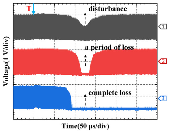
Figure 13.
The disturbance (signal 1), a period of loss (signal 2), and complete loss (signal 3) of FPGA IO 50 MHz for the negative PCI into 3.3 V power line of JXCV5SX95T test board. The auto-reconfiguration process occurs after the complete loss.
3.2.3. Injection into 2.5 V Power Line
HF outputs of only DLLs exhibit faults for positive PCI into the 2.5 V power line. However, during the negative PCI, HF outputs of various clock resources (GCBs, DLLs, and PLLs) all have faults, which also manifest as the temporary loss, but the loss waveforms are different from those in the positive PCI. Their failure thresholds are summarized in Table 4. The configuration frequency, resource type, and location constraint of clock resources are three important factors affecting their sensitivity.
Table 4.
Failure thresholds of HF outputs for the negative PCI into the 2.5 V power line of JXCV5SX95T test board.
Firstly, for the same type of resource (DLL or PLL), the higher the frequency, the more sensitive it is. On the one hand, it is clear from Table 4 that the higher frequency has the lower failure threshold. On the other hand, Figure 14 shows the HF outputs of DLLs and PLLs at different configuration frequencies for a −62.2 A PCI; the higher the frequency, the longer the loss. Secondly, HF outputs of the same frequency but different resource types present different sensitivities. For example, FPGA GCB, FPGA DLL + GCB, and FPGA PLL + GCB of 50 MHz have different failure thresholds. Thirdly, although both FPGA BUFG and ADC_CLK at 50 MHz utilize GCB, their location constraints are different, leading to different failure thresholds. Thus, for resources of the same frequency and type, location constraints may also affect their sensitivity.
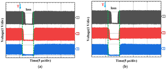
Figure 14.
Longer losses of FPGA GCB + DLL and FPGA GCB + PLL with higher frequencies for −62.2 A PCI into the 2.5 V power line of JXCV5SX95T test board, (a) FPGA GCB + DLL with 25 MHz (signal 1), 50 MHz (signal 2), and 100 MHz (signal 3) and (b) FPGA GCB + PLL with 25 MHz (signal 1), 50 MHz (signal 2), and 100 MHz (signal 3).
3.2.4. Injection into 1.1 V Power Line
The 1.1V power line supplies the internal voltage (VCCINT) of JXCV5SX95T. None of the output faults were investigated during the positive PCI. However, all HF outputs have a period of loss as the negative injection amplitude increases. Table 5 summarizes the failure stages and thresholds, revealing that the configuration frequency of the resource is the main influencing factor on the sensitivity, and that HF outputs of higher frequency are more sensitive. All HF outputs of the same frequency have the same failure threshold. Figure 15 illustrates the HF outputs of DLLs and PLLs at different frequencies when the injection amplitude is −82.6 A, and higher frequencies correspond to longer loss.
Table 5.
Failure stages and thresholds of the negative PCI into 1.1V power line of the JXCV5SX95T test board.
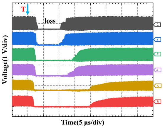
Figure 15.
Longer losses of FPGA GCB + DLL with 25 MHz (signal 1), 50 MHz (signal 3), and 100 MHz (signal 5) and FPGA GCB + PLL with 25 MHz (signal 2), 50 MHz (signal 4), and 100 MHz (signal 6) for −82.6 A PCI into 1.1 V power line of JXCV5SX95T test board.
3.3. The Comparison of JXCV5SX95T and XC5VSX95T
Table 6 compares the EMP sensitivity for the power modules of two FPGAs (JXCV5SX95T and XC5VSX95T). There are obvious differences only in the negative PCI into the 1.1 V power line, manifesting as different failure characteristics and thresholds.
Table 6.
Comparison results of EMP sensitivity for power lines JXCV5SX95T and XC5VSX95T.
The 1.1 V power line also supplies the internal voltage (VCCINT) of the XC5VSX95T. During negative PCI, as the injection amplitude increases, all HF outputs, except for DAC_SYNC_OUT, experience multiple periods of loss. Figure 16 shows some typical HF outputs with three periods of loss, and they have the same duration of loss. FPGA IO, FPGA GCB, and ADC_CLK have losses and disturbances, while other HF outputs have only losses. The above failure characteristics are quite similar to those in the case of PCI into the 3.3 V power line of the JXCV5SX95T test board. This suggests that the sensitive circuit for negative PCI into the 1.1 V power line of the XC5VSX95T should be at the input section of sys_clk. However, the failure thresholds of PCI into the 1.1 V power line of the JXCV5SX95T are significantly related to the configuration frequency; the corresponding sensitive location could be in the structural circuit of each resource. Therefore, due to the different manufacturing processes, the VCCINT of the two FPGAs has different sensitive circuit locations for EMP and exhibits different failure characteristics and thresholds.
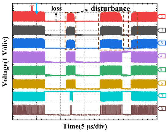
Figure 16.
ALL HF outputs with three periods of loss except DAC_SYNC_OUT for the negative PCI into 1.1 V power line of XC5VSX95T test board. FPGA GCB + PLL and FPGA GCB + DLL with the same frequency have the same failure characteristics. Only FPGA IO, FPGA GCB, and ADC_CLK have disturbance. Signals 1, 2, 3, 4, 5, 6, 7, and 8 correspond to FPGA IO, FPGA GCB, ADC_CLK, FPGA GCB + DLL 25 MHz, FPGA GCB + DLL 50 MHz, FPGA GCB + DLL 100 MHz, ADC_CLKOUT 50 MHz, and ADC sine-to-square 10 MHz, respectively.
4. Discussion
According to the experimental results, the four power modules of two FPGAs (JXCV5SX95T or XCV5SX95T), including input port voltage, output port voltage, auxiliary voltage (VCCAUX), and internal voltage (VCCINT), exhibit significantly different failure characteristics and thresholds. The sensitive sub-circuits of these power modules are located at different positions in the FPGAs. Consequently, the effects caused by PCI on FPGAs exhibit significant differences, leading to distinct failure waveforms at the same output.
When two FPGAs operate under the configuration program, their internal resources frequently and simultaneously switch between different logic levels, causing transient current fluctuations on the corresponding power distribution networks (PDNs). Furthermore, the parasitic inductance of PDNs can induce voltage fluctuation, generating synchronous switching noise (SSN) [34]. As the operating frequency increases, the level switching is faster and the amplitude of voltage fluctuation increases significantly, resulting in FPGAs having a lower power supply noise tolerance. Therefore, FPGAs will be more sensitive to external electromagnetic interference. In this context, the injected 20/500ns double-exponential pulsed current has a faster pulse edge that also can induce transient voltage fluctuation on the PDN, which couples with SSN to further affect power integrity (PI). Especially at higher frequencies, this superposition effect can have a more significant impact on the stability and performance of FPGAs. Therefore, reducing the operating frequency will improve the performance of FPGAs in the EMP environment.
The experimental results show that compared to the port voltage, VCCAUX and VCCINT have significantly more different sensitivities to PCIs with different polarities. Under negative PCI, they even have more complex failure stages or characteristics, which deserves sufficient attention. However, sensitivity investigations into different injection polarities seem to be rare in previous PCI reports about electronic devices. Moreover, different processes can change the location of the sensitive circuits for VCCINT, leading to different impact mechanisms on FPGAs and consequently causing different output failure features. Furthermore, one of the main differences between modern FPGAs and the samples in this experiment is the manufacturing process. The comparative study of two FPGAs provides basic data and theoretical reference for the EMP sensitivity study of more advanced FPGAs.
The experimental results and analysis indicate that the parasitic inductance of PDN is one of the critical factors affecting the stable operations of two FPGAs. An increase in parasitic inductance directly leads to a higher noise amplitude on the power plane, which impacts the performance of FPGAs. Therefore, optimizing the PDN design to reduce parasitic inductance is important, such as increasing the area of the power plane, reducing the distance between the power and ground layers, and minimizing the number of vias on the power planes. In addition, from the perspective of electromagnetic protection, previous studies have shown that capacitors on the PDN have a significant filtering effect on the external pulse current, and thus can improve the electromagnetic compatibility (EMC) and interference immunity of FPGAs [15]. In this experiment, a 10 μF capacitor was added onto the VCCINT PDN of the test board. As shown in Figure 17, the filtering effect is evaluated by monitoring changes in the waveform of the pulsed current before and after filtering. It can be seen that the filtering effect of the high-value capacitor is reflected in two aspects. On the one hand, it effectively reduces the amplitude of the pulsed current. On the other hand, it slows down the pulse edge, thus improving the EMP sensitivity.
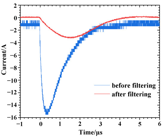
Figure 17.
Pulse current waveforms before and after filtering with a 10 μF capacitor.
During the experiment, some conditions may change, potentially affecting the test results. Firstly, prolonged operation can cause the FPGA chip temperature to rise, which may affect the experimental results. Secondly, complex transient electromagnetic fields could be present in the environment, affecting the performance of FPGA, especially when it is operating at high frequencies. Therefore, coaxial cables were used for signal transmission. Additionally, even if the parameter settings of the pulsed current generator are the same, there may still be slight variations in the output amplitude and rise and fall time. To mitigate these effects, the number of test samples and pulse injection repetitions were increased to improve the reliability and repeatability of the data.
5. Conclusions
In this paper, the PCI method is adopted to investigate the EMP sensitivity of power modules of FPGAs experimentally. It is found that different power modules have significantly different EMP sensitivities. For each power module, HF signals are more sensitive than constant signals in most cases, and frequency is an important factor in sensitivity. In addition, the EMP sensitivity of the VCCAUX can also be affected by resource types and location constraints, thus requiring a comprehensive assessment. All power modules exhibit different sensitivities to PCIs of different polarities. The manufacturing processes of FPGAs have a slight effect on the EMP sensitivity of their power modules, which is only reflected on the VCCINT. Moreover, in the case of enabled PROM, an auto-reconfiguration process is observed for the first time. However, the mechanisms of some specific output failures have not been revealed deeply. The EMP sensitivity of other types, especially more advanced FPGAs, still needs to be further investigated. The effect of capacitance in improving EMP sensitivity needs to be further investigated. These aspects will be the focus of future research.
Author Contributions
Conceptualization, Y.L. (Yang Li); methodology, N.L., C.M. and F.Q.; validation, N.L; formal analysis, N.L.; investigation, N.L. and Z.P.; resources, C.H. and Y.L. (Yonghong Li); data curation, Z.P.; writing—original draft preparation, N.L.; writing—review and editing, N.L., Z.P., Y.L. (Yang Li), Y.L. (Yonghong Li), P.L., W.Y., H.B., J.L., B.H. and C.H.; visualization, N.L. and C.H.; supervision, C.H.; project administration, C.H. All authors have read and agreed to the published version of the manuscript.
Funding
This research was funded by the National Natural Science Foundation of China (Grant No. 12275211, 11835006) and the State Key Laboratory of Intense Pulsed Radiation Simulation and Effect (Grant No. SKLIPR2201).
Data Availability Statement
Data are contained within the article.
Conflicts of Interest
The authors declare no conflict of interest.
References
- Fleetwood, D.M. Radiation Effects in a Post-Moore World. IEEE Trans. Nucl. Sci. 2021, 68, 509–545. [Google Scholar] [CrossRef]
- Darwish, M.N.; Dolly, M.C.; Goodwin, C.A.; Titus, J.L. Radiation Effects on Power Integrated Circuits. IEEE Trans. Nucl. Sci. 1988, 35, 1547–1551. [Google Scholar] [CrossRef]
- Bezhenova, V.; Michalowska-Forsyth, A.M. Effects of Ionizing Radiation on Integrated Circuits. Elektrotech. Inftech. 2016, 133, 39–42. [Google Scholar] [CrossRef]
- Ferlet-Cavrois, V.; Massengill, L.W.; Gouker, P. Single Event Transients in Digital CMOS—A Review. IEEE Trans. Nucl. Sci. 2013, 60, 1767–1790. [Google Scholar] [CrossRef]
- Lee, M.; Cho, S.; Lee, N.; Kim, J. Design for High Reliability of CMOS IC With Tolerance on Total Ionizing Dose Effect. IEEE Trans. Device Mater. Reliab. 2020, 20, 459–467. [Google Scholar] [CrossRef]
- Guo, Y.; Li, Y.; Li, J.; He, C.; Li, R.; Li, Y.; Li, P.; Liu, J. Experimental Study of Transient Dose Rate Effects of Two Level-Shifting Transceivers and Simulations on Their ESD Circuits. IEEE Trans. Nucl. Sci. 2022, 69, 1157–1166. [Google Scholar] [CrossRef]
- Hao, R.; Zhang, X.; Gao, H.; Wu, H.; Cheng, J.; Li, G.-P. A Novel High-Altitude Electromagnetic Pulse (HEMP) Protection Circuit for RF Applications. Microelectron. J. 2019, 84, 1–8. [Google Scholar] [CrossRef]
- Hoad, R.; Radasky, W.A. Progress in High-Altitude Electromagnetic Pulse (HEMP) Standardization. IEEE Trans. Electromagn. Compat. 2013, 55, 532–538. [Google Scholar] [CrossRef]
- Xie, H.; Liu, Y.; Li, Y.; Qiao, H. A Prediction Model Based on Artificial Neural Network for E1 HEMP Coupling With Distribution Power Lines. IEEE Trans. Power Deliv. 2022, 37, 5337–5344. [Google Scholar] [CrossRef]
- Giri, D.V.; Prather, W.D. High-Altitude Electromagnetic Pulse (HEMP) Risetime Evolution of Technology and Standards Exclusively for E1 Environment. IEEE Trans. Electromagn. Compat. 2013, 55, 484–491. [Google Scholar] [CrossRef]
- Li, C.; Liu, Y.; Liu, J.; Wei, A.; En, Y. Electromagnetic Interference Effects in the Bipolar Voltage Comparators. In Proceedings of the 10th International Conference on Reliability, Maintainability and Safety (ICRMS), Guangzhou, China, 6–8 August 2014; pp. 185–188. [Google Scholar]
- Feng, Y.; Sun, L.; Lu, J.; Li, Z.; Tian, J.; Qiu, Y. Equivalent Circuit and Damage Threshold Study of Communication Interfaces under HEMP. J. Electron. Test. 2024, 40, 615–624. [Google Scholar] [CrossRef]
- Du, C.; Xia, D.; Huang, Q.; Mao, C.; Cui, Z.; Fang, W.; Nie, X. Research on Electromagnetic Susceptibility of Electronic Modules in Component-Level HEMP PCI Test. Energies 2022, 15, 1409. [Google Scholar] [CrossRef]
- Li, B.; Boyer, A.; Bendhia, S.; Lemoine, C. Ageing Effect on Electromagnetic Susceptibility of a Phase Locked Loop. Microelectron. Reliab. 2010, 50, 1304–1308. [Google Scholar] [CrossRef]
- Kwak, S.; Nah, W.; Kim, S. Electromagnetic Susceptibility Analysis of I/O Buffers Using the Bulk Current Injection Method. J. Semicond. Technol. Sci. 2013, 13, 114–126. [Google Scholar] [CrossRef]
- Park, I.; Jang, I.; Jung, W.; Kim, S. Noise Immunity Modeling and Analysis of Delay-Locked Loop. In Proceedings of the 2015 IEEE 19th Workshop on Signal and Power Integrity (SPI), Berlin, Germany, 10 May 2015; pp. 1–4. [Google Scholar]
- Junping, C.; Changlin, Z.; Daojie, Y.; Zhijian, X.; Dongyao, Z. Electromagnetic susceptibility analysis of FPGA based on conducted coupling of power supply network. High Power Laser Part Beams 2019, 31, 023202–023207. [Google Scholar] [CrossRef]
- Swaminathan, M.; Chung, D.; Grivet-Talocia, S.; Bharath, K.; Laddha, V.; Xie, J. Designing and Modeling for Power Integrity. IEEE Trans. Electromagn. Compat. 2010, 52, 288–310. [Google Scholar] [CrossRef]
- Wu, T.-L.; Chuang, H.-H.; Wang, T.-K. Overview of Power Integrity Solutions on Package and PCB: Decoupling and EBG Isolation. IEEE Trans. Electromagn. Compat. 2010, 52, 346–356. [Google Scholar] [CrossRef]
- Jagadeesh, R.B.; Ramashastry, V.; Ramprasad, B.; Srihari, S.P.R.B.; Bhat, S.; Radhakrishna, V.S. IC Package with the System Board Interconnects—Simulation Showing PDN Noise Due to Simultaneous Switching IOs and Its Effect on Signal Integrity. In Proceedings of the 2022 IEEE Electrical Design of Advanced Packaging and Systems (EDAPS), Urbana, IL, USA, 12–14 December 2022; pp. 1–3. [Google Scholar]
- Wu, P.; Xu, Z.; Meng, C.; Wen, L.; Guo, Q. The Experiment Study of Effects on ADC Chip against Radiation and Electromagnetic Environment. In Proceedings of the 12th International Workshop on the Electromagnetic Compatibility of Integrated Circuits (EMC Compo), Hangzhou, China, 1 October 2019; pp. 207–209. [Google Scholar]
- Xu, X.-C.; Han, C.-Y.; Shao, E.; Lu, X.-J.; Fang, W.-X.; Chen, R.-Q.; Liu, H.-Z.; Shao, W.-H.; Shi, Y.-L. Study of the HPM Interference Effect on Integrated Circuit in a TEM Cell. In Proceedings of the 2019 International Conference on Quality, Reliability, Risk, Maintenance, and Safety Engineering (QR2MSE), Zhangjiajie, China, 6–9 August 2019; pp. 1–7. [Google Scholar]
- Zhou, Y.; Xie, Y.-Z.; Zhang, D.-Z.; Jing, Y. Modeling and Performance Evaluation of Inductive Couplers for Pulsed Current Injection. IEEE Trans. Electromagn. Compat. 2021, 63, 710–719. [Google Scholar] [CrossRef]
- Cui, Z.; Grassi, F.; Pignari, S.A.; Wei, B. Pulsed Current Injection Setup and Procedure to Reproduce Intense Transient Electromagnetic Disturbances. IEEE Trans. Electromagn. Compat. 2018, 60, 2065–2068. [Google Scholar] [CrossRef]
- XC5VSX95T-1FF1136C Xilinx Inc.|Integrated Circuits (ICs)|DigiKey. Available online: https://www.digikey.com/en/products/detail/amd/XC5VSX95T-1FFG1136C/1768662 (accessed on 22 June 2022).
- Vera, A.; Llamocca, D.; Pattichis, M.; Kemp, W.; Shedd, W.; Alexander, D.; Lyke, J. Dose Rate Upset Investigations on the Xilinx Virtex IV Field Programmable Gate Arrays. In Proceedings of the 2007 IEEE Radiation Effects Data Workshop, Honolulu, HI, USA, 23–27 July 2007; pp. 172–176. [Google Scholar]
- Vera, A.; Llamocca, D.; Fabula, J.; Kemp, W.; Marquez, R.; Shedd, W.; Alexander, D. Xilinx Virtex V Field Programmable Gate Array Dose Rate Upset Investigations. In Proceedings of the 2008 IEEE Radiation Effects Data Workshop, Tucson, AZ, USA, 14–18 July 2008; pp. 90–93. [Google Scholar]
- Li, Y.; Li, J.; Guo, Y.; He, C.; Li, R.; Chen, W.; Liao, W.; Li, Y.; Li, P.; Liu, J.; et al. Experimental Study of Transient Dose Rate Effect on System-in-Package SZ0501. IEEE Trans. Nucl. Sci. 2022, 69, 1840–1849. [Google Scholar] [CrossRef]
- Li, Y.; Guo, Y.; Li, J.; He, C.; Peng, Z.; Liu, J.; Li, R.; Zhao, H.; Chen, W.; Li, Y.; et al. Transient Dose Rate Effect Between System-in-Package and Printed Circuit Boards: A Comparative Experimental Study. IEEE Trans. Nucl. Sci. 2023, 70, 2106–2115. [Google Scholar] [CrossRef]
- Zhou, Y.; Xie, Y.; Zhang, D. Performance Evaluation of Inductive and Capacitive Couplers for Pulsed Current Injection. IEEE Trans. Electromagn. Compat. 2022, 64, 85–91. [Google Scholar] [CrossRef]
- Tang, K.T.; Friedman, E.G. Simultaneous Switching Noise in On-Chip CMOS Power Distribution Networks. IEEE Trans. Very Large Scale Integr. (VLSI) Syst. 2002, 10, 487–493. [Google Scholar] [CrossRef]
- Li, N.; Li, Y.; Guo, Y.; He, C. Simulation Analysis of Electromagnetic Pulse Susceptibility and Hardening Design for System-in-Package SZ0501. Microelectron. Reliab. 2023, 141, 114892. [Google Scholar] [CrossRef]
- Li, J.; Li, Y.; Guo, Y.; Li, R.; Chen, W.; Liu, Y.; Peng, Z.; Liu, J.; He, C.; Li, P. Investigation of Transient Dose-Rate Effect on High-Speed Comparator SB9696. IEEE Trans. Nucl. Sci. 2023, 70, 1459–1469. [Google Scholar] [CrossRef]
- Shenglong, W.; Ling, S.; Haiyan, S.; Lingling, Y.; Boyuan, Z.; Junwei, L. Relationship between SSN and EMC in SiP. In Proceedings of the 14th International Conference on Electronic Packaging Technology, Dalian, China, 11–14 August 2013; pp. 622–625. [Google Scholar]
Disclaimer/Publisher’s Note: The statements, opinions and data contained in all publications are solely those of the individual author(s) and contributor(s) and not of MDPI and/or the editor(s). MDPI and/or the editor(s) disclaim responsibility for any injury to people or property resulting from any ideas, methods, instructions or products referred to in the content. |
© 2025 by the authors. Licensee MDPI, Basel, Switzerland. This article is an open access article distributed under the terms and conditions of the Creative Commons Attribution (CC BY) license (https://creativecommons.org/licenses/by/4.0/).