
DMR-SCL: A Design and Verification Framework for Redundancy-Based Resilient Asynchronous Sleep Convention Logic Circuits †


Abstract
1. Introduction
- A redundancy-based error-tolerant SCL architecture has been introduced.
- A categorical proof is presented to illustrate the proposed architecture’s ability to fully recover from an SEU or SEL without compromising functionality.
- The performance of the proposed architecture is evaluated and compared to an existing NCL-resilient scheme on four crucial fronts: transistor count, energy utilization per operation, idle stage power dissipation, and latency.
- A scalable verification scheme is developed for the proposed architecture. QDI asynchronous circuits are generally synthesized from their corresponding synchronous specifications utilizing design automation tools. During the process, the circuit undergoes substantial modification, resulting in an implementation that differs significantly from the specification. We have formalized a verification framework based on equivalence checking, which can verify the safety (functional correctness) as well as the liveness (the absence of deadlock/livelock) of the synthesized error-resilient SCL circuits that are designed based on the proposed architecture.
2. Background and Related Work
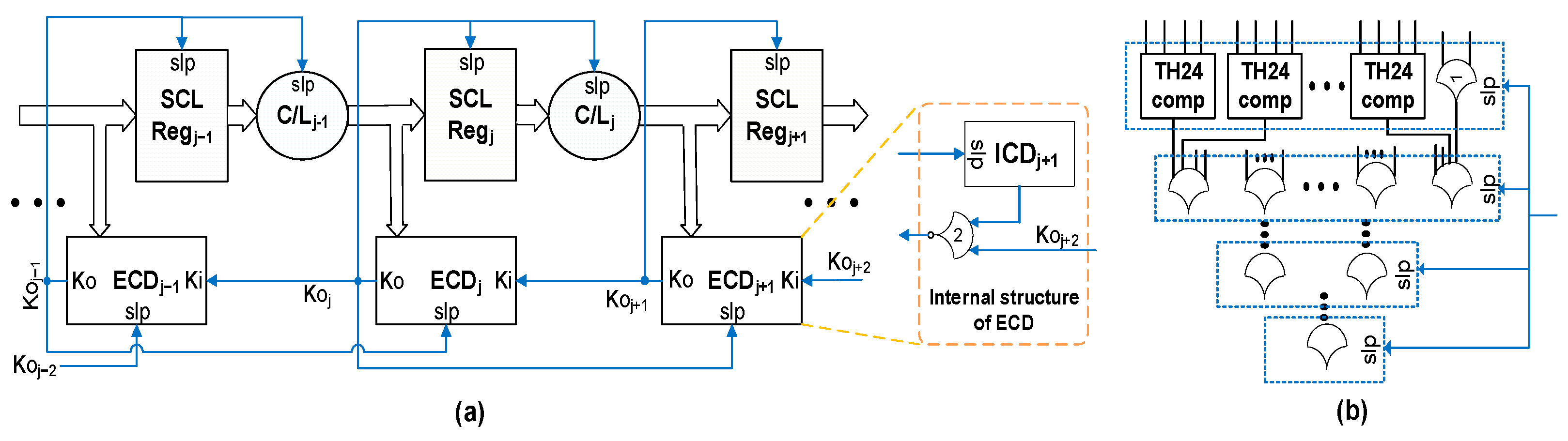
2.1. Conventional SCL Architecture
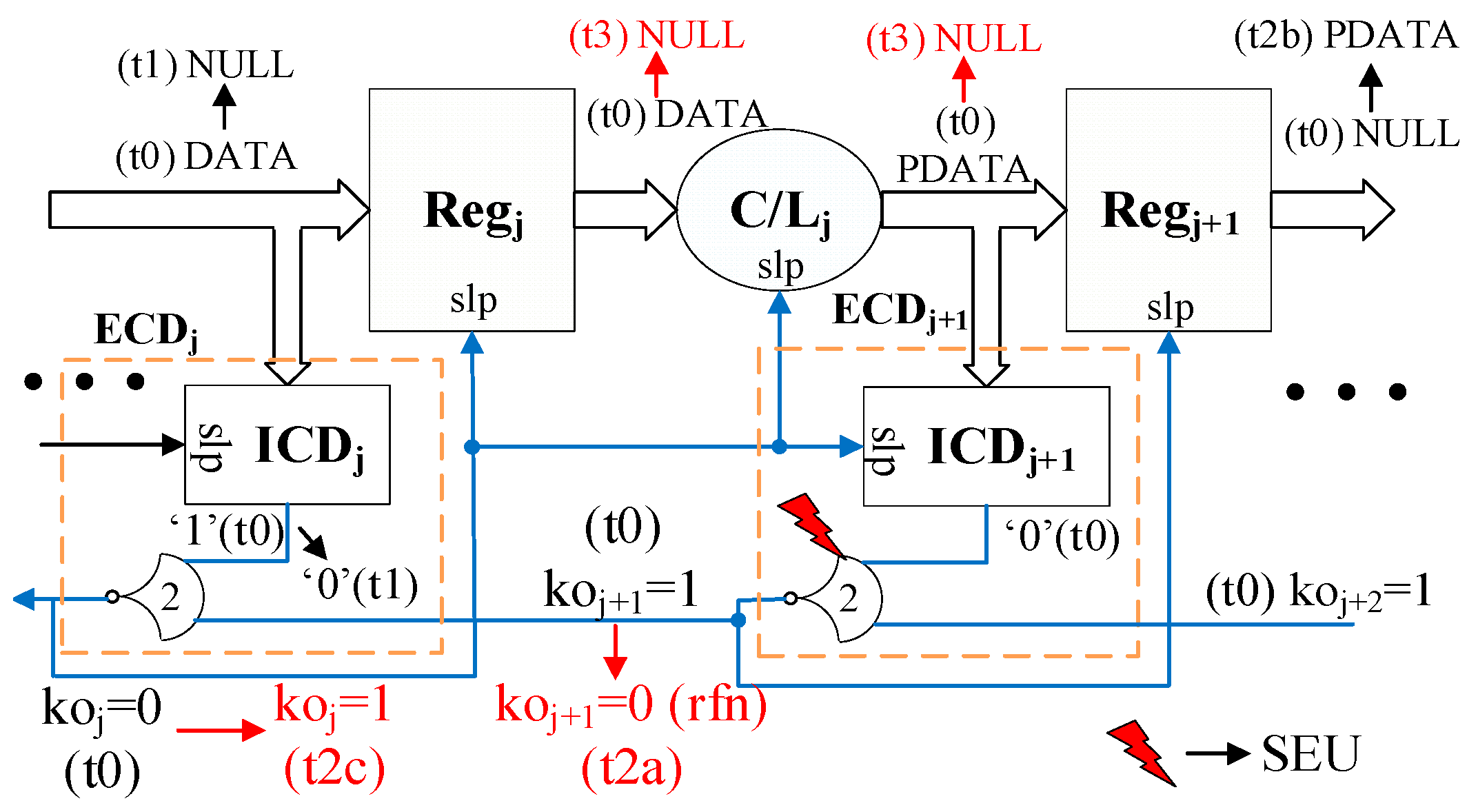
2.2. Impact of Single-Event Effects on SCL Circuits
2.3. Resilient and Radiation-Hardened QDI Architectures
3. Error-Resilient SCL Circuit Design
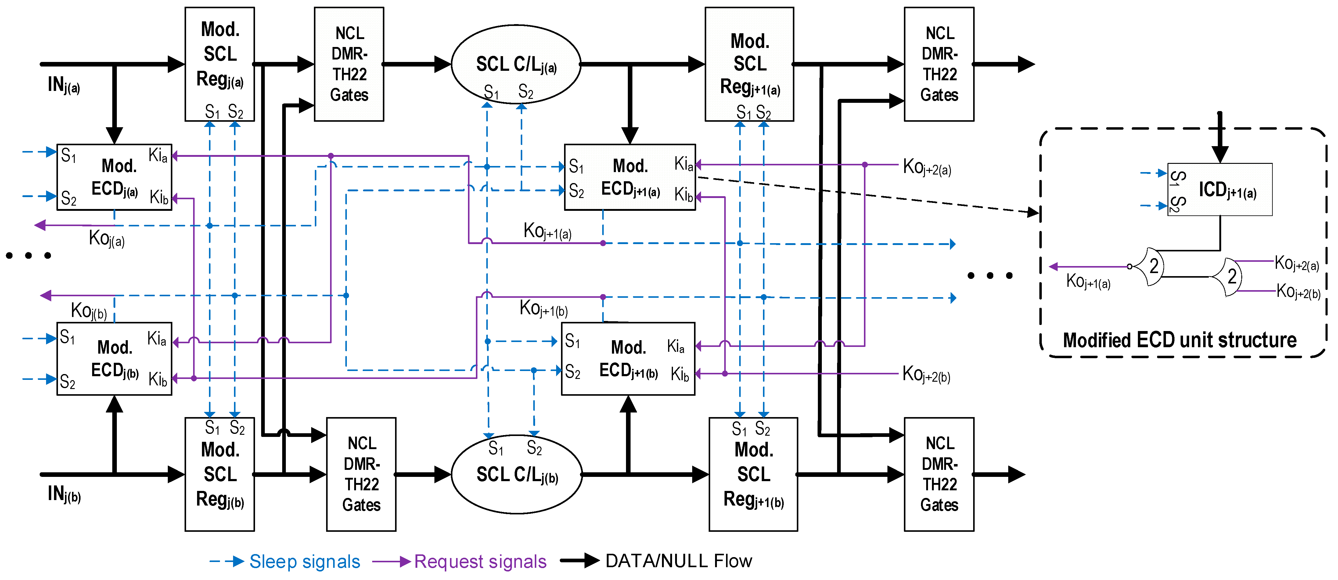
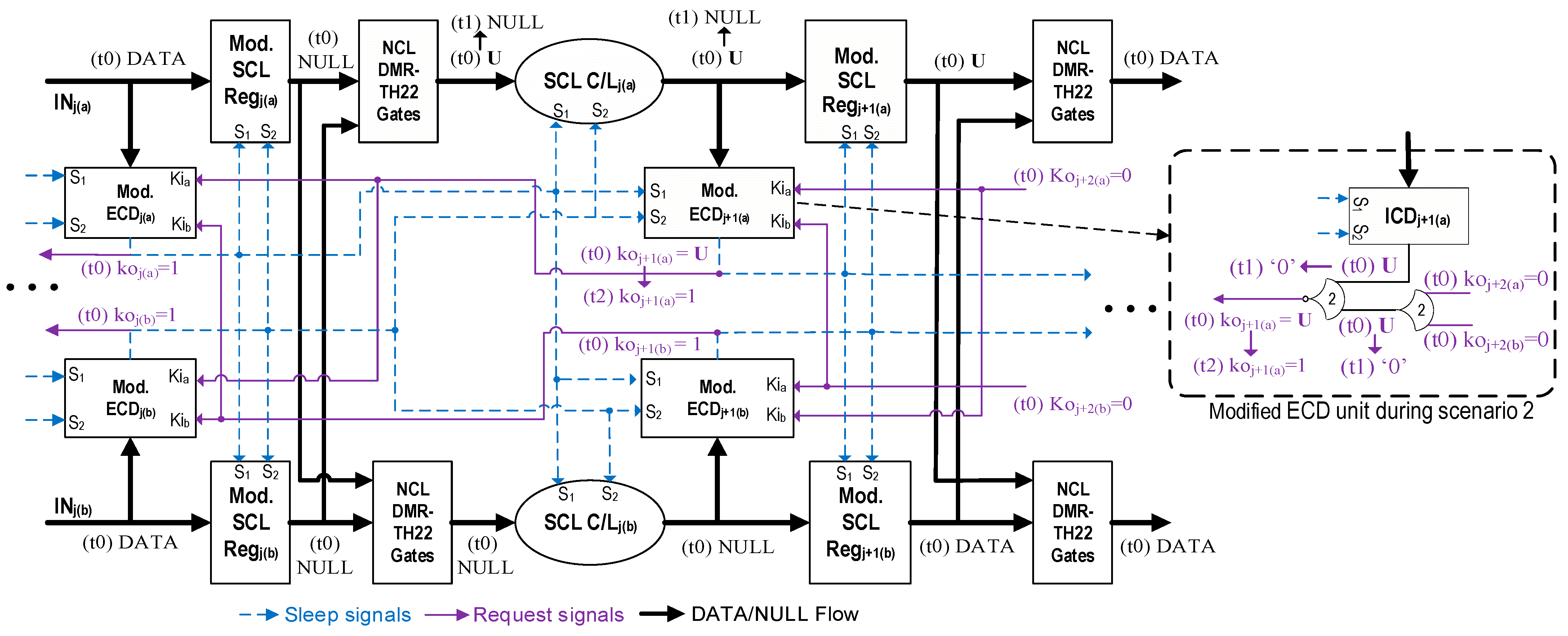
3.1. Proposed SEL/SEU-Resistant SCL Architecture
- The original SCL pipeline is doubled.At the output of the registers in each stage, a series of additional NCL TH22 gates with hysteresis (referred to herein as DMR-TH22 gates) are added, which accept register outputs from both copies in the same stage as inputs. For instance, consider, in the original copy, a 1-bit SCL register with dual-rail input, D, and dual-rail output, F. The input and output of the corresponding duplicate register are Ds and Fs, respectively (note that ‘s’ in the signal name indicates that the signal is from the shadow/duplicate circuit. This convention will be followed throughout the paper). There will be two NCL-TH22 gates following the registers, one of which will have F.rail0 and Fs.rail0 as inputs, while the other will have F.rail1 and Fs.rail1 as inputs. The C-element [25] nature of NCL TH22 gates ensures that for each stage, the register outputs of both the circuits must match to allow further propagation.
- Each register, C/L, and ICD unit is modified to accept two sleep signals, one from each copy. This is accomplished by adding two extra transistors (one PMOS and one NMOS) to the SCL gates and registers, as shown in Figure 4, preventing the gates from sleeping until both sleep signals are asserted.
- One additional NCL TH22 gate is added before the inverting NCL TH22 (TH22n) gate in each ECD unit, which accepts the Ko outputs generated by the subsequent stage ECDs from both the original and duplicate copies, as shown in Figure 3.
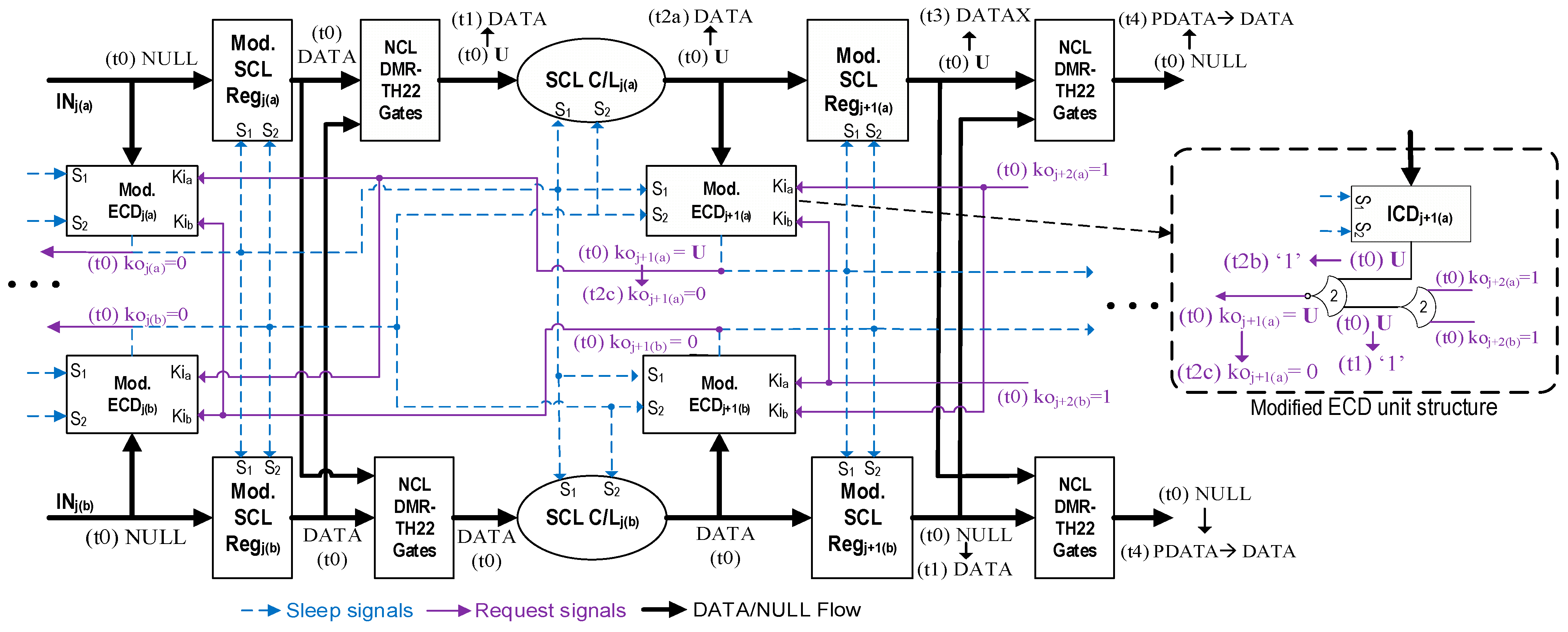
3.2. Recovering from Single-Event Effects Without Compromising Safety
3.2.1. SCL Recovery Under Scenario 1
3.2.2. SCL Recovery Under Scenario 2
3.3. Recovering from Single-Event Effects Without Compromising Liveness
4. Simulation Results
4.1. DMR-NCL vs. DMR-SCL: Performance Evaluation and Comparison
- DMR-NCL circuits have an area overhead compared to DMR-SCL circuits. This is because NCL gates require more transistors than the modified DMR-SCL gates with two sleep inputs. Also, DMR-NCL register structures require more transistors than DMR-SCL registers. Therefore, for pipelined implementations, the area savings in DMR-SCL will be even more than DMR-NCL.
- DMR-NCL requires the propagation of a complete NULL wavefront through all the C/L, registers, and completion components in a stage after a DATA propagation, whereas the DATA-to-NULL transition in DMR-SCL is achieved through sleep inputs without the need for a separate NULL wavefront propagation. This results in much fewer switching activities during the NULL transition, reducing the overall energy utilization. In addition, the SCL gates are more energy-efficient due to the integration of MTCMOS technology, which further reduces the energy utilization.
- Despite requiring theoretically less time in the DATA-to-NULL transition, the latency overhead of DMR-SCL circuits has been found to be more than that of DMR-NCL circuits in our simulation. This can be attributed to the inclusion of high-threshold transistors in the SCL gates, resulting in slower switching compared to NCL gates. The speed of the DMR-SCL operation can be further enhanced by determining the optimal transistor sizing and threshold voltage. Also note that the circuits in Table 1 are not pipelined. In finer pipelined implementations, the latency of DMR-NCL is anticipated to have more overhead due to the propagation of the NULL wavefront across all stages [17].
- The integration of MTCMOS technology results in a substantial reduction in leakage in DMR-SCL circuits compared to DMR-NCL circuits, rendering them appropriate for applications that remain idle for an extended period.
4.2. DMR-SCL vs. SCL: Analysis of Overhead
5. Verification Framework for the SEL/SEU-Resistant SCL Architecture
5.1. Safety Check Procedure
- P1:
- P2: (,…, ) = SCLBoolStep
- P3: (,…, ) = SCLBoolStep
- P4:
- P5:
- PO1a:
- PO1b:
5.2. Handshaking and Liveness Check Procedure
6. Verification Results and Discussion
7. Conclusions and Future Work
- The proposed DMR-SCL architecture, in its current form, cannot handle concurrent multi-event upsets (MEUs). For example, a deadlock may still occur if both ECD outputs of a specific stage (original and duplicate) are corrupted simultaneously. However, the proposed architecture can be modified to tackle MEUs, which is an area of future research.
- Extensive simulations ensure that the proposed DMR-SCL architecture can mitigate the single-event effects correctly. A hardware implementation with a proper experimental setup would be beneficial to test the architecture in the presence of radiation.
- The proposed verification scheme is directly applicable to the verification of any combinational DMR-SCL circuits, as discussed in Section 6, and, with minor modifications, can be used to verify sequential DMR-SCL circuits without interactive feedback loops. However, this method would require advanced register mapping algorithms to be applicable to verify any arbitrary sequential DMR circuits with interactive loops, which will be addressed in our future research.
- In place of an SAT solver, we intend to utilize commercial equivalence checkers (e.g., Jasper Gold SEC) to enhance the scalability of the verification method and validate larger sequential benchmarks.
Author Contributions
Funding
Data Availability Statement
Conflicts of Interest
Abbreviations
| QDI | Quasi-delay-insensitive (QDI) |
| NCL | Null Convention Logic |
| SCL | Sleep Convention Logic |
| SEU | Single-event upset |
| SEL | Single-event latch-up |
| SEE | Single-event effect |
| EMI | Electromagnetic Interference |
| MTNCL | Multi-threshold NCL |
| MTCMOS | Multi-threshold complementary metal oxide semiconductor |
| ICD | Internal completion detection |
| ECD | Early-completion detection |
| TMR | Triple-modular redundancy |
| DMR | Dual-modular redundancy |
| ECC | Error correcting code |
| SMT | Satisfiability Modulo Theory |
References
- Baumann, R. Soft errors in advanced computer systems. IEEE Des. Test Comput. 2005, 22, 258–266. [Google Scholar] [CrossRef]
- Dodd, P.E.; Massengill, L.W. Basic mechanisms and modeling of single-event upset in digital microelectronics. IEEE Trans. Nucl. Sci. 2003, 50, 583–602. [Google Scholar] [CrossRef]
- Shoga, M.; Binder, D. Theory of single event latchup in complementary metal oxide semiconductor circuits. IEEE Trans. Nucl. Sci. 1986, 33, 1714–1717. [Google Scholar] [CrossRef]
- Weaver, C.; Emer, J.; Mukherjee, S.S.; Reinhardt, S.K. Techniques to reduce the soft error rate of a high-performance microprocessor. ACM SIGARCH Comput. Archit. News 2004, 32, 264. [Google Scholar] [CrossRef]
- Sakib, A.A. Soft error tolerant quasi-delay insensitive asynchronous circuits: Advancements and challenges. In Proceedings of the 34th SBC/SBMicro/IEEE/ACM Symposium on Integrated Circuits and Systems Design (SBCCI), Campinas, Brazil, 23–27 August 2021; pp. 1–6. [Google Scholar]
- Fant, K.M.; Brandt, S.A. Null convention logic: A complete and consistent logic for asynchronous digital circuit synthesis. In Proceedings of the International Conference on Application Specific Systems, Architectures and Processors: ASAP’96, Chicago, IL, USA, 19–21 August 1996; pp. 261–273. [Google Scholar]
- Di, J.; Smith, S.C. (Eds.) Asynchronous Circuit Applications; IET: Stevenage, UK, 2019; Available online: https://digital-library.theiet.org/content/books/cs/pbcs061e (accessed on 1 December 2024).
- Zhou, L.; Parameswaran, R.; Parsan, F.A.; Smith, S.C.; Di, J. Multi-Threshold NULL Convention Logic (MTNCL): An ultra-low power asynchronous circuit design methodology. J. Low Power Electron. Appl. 2015, 5, 81–100. [Google Scholar] [CrossRef]
- Smith, S.C.; Di, J. Designing Asynchronous Circuits Using NULL Convention Logic (NCL); Morgan & Claypool: San Rafael, CA, USA, 2009. [Google Scholar]
- Zhou, L.; Smith, S.C.; Di, J. Bitwise MTNCL: An ultra-low power bit-wise pipelined asynchronous circuit design methodology. In Proceedings of the 53rd IEEE International Midwest Symposium on Circuits and Systems, Seattle, WA, USA, 1–4 August 2010; pp. 217–220. [Google Scholar]
- Alzahrani, A.; Bailey, A.D.; Fu, G.; Di, J. Glitch-Free Design for Multi-Threshold CMOS NCL Circuits. In Proceedings of the ACM 2009 Great Lakes Symposium on VLSI, Boston, MA, USA, 10–12 May 2009. [Google Scholar]
- Khodosevych, D.; Sakib, A.A. Evolution of NULL convention logic based asynchronous paradigm: An overview and outlook. IEEE Access 2022, 10, 78650–78666. [Google Scholar] [CrossRef]
- Smith, S.C. Speedup of Self-Timed Digital Systems Using Early Completion. In Proceedings of the IEEE Computer Society Annual Symposium on VLSI, Pittsburgh, PA, USA, 25–26 April 2002; pp. 107–113. [Google Scholar]
- Kao, J.T.; Chandrakasan, A.P. Dual-threshold voltage techniques for low-power digital circuits. IEEE J. Solid-State Circuits 2000, 35, 1009–1018. [Google Scholar] [CrossRef]
- Hossain, M.; Sakib, A.A.; Srinivasan, S.K.; Smith, S.C. An equivalence verification methodology for asynchronous sleep convention logic circuits. In Proceedings of the 2019 IEEE International Symposium on Circuits and Systems (ISCAS), Sapporo, Japan, 26–29 May 2019; pp. 1–5. [Google Scholar]
- Kuang, W.; Zhao, P.; Yuan, J.S.; DeMara, R.F. Design of asynchronous circuits for high soft error tolerance in deep submicrometer CMOS circuits. IEEE Trans. Very Large-Scale Integr. (VLSI) Syst. 2010, 18, 410–422. [Google Scholar] [CrossRef]
- Zhou, L.; Smith, S.; Di, J. Radiation Hardened NULL Convention Logic Asynchronous Circuit Design. J. Low Power Electron. Appl. 2015, 5, 216–233. [Google Scholar] [CrossRef]
- Lyons, R.E.; Vanderkulk, W. The use of triple-modular redundancy to improve computer reliability. IBM J. Res. Dev. 1962, 6, 200–209. [Google Scholar] [CrossRef]
- Jang, W.; Martin, A.J. SEU-tolerant QDI circuits [quasi delay-insensitive asynchronous circuits]. In Proceedings of the 11th IEEE International Symposium on Asynchronous Circuits and Systems, New York, NY, USA, 14–16 March 2005; pp. 156–165. [Google Scholar]
- Lodhi, F.K.; Hasan, O.; Hasan, S.R.; Awwad, F. Modified null convention logic pipeline to detect soft errors in both null and data phases. In Proceedings of the IEEE 55th International Midwest Symposium on Circuits and Systems (MWSCAS), Boise, ID, USA, 5–8 August 2012; pp. 402–405. [Google Scholar]
- Lodhi, F.K.; Hasan, S.R.; Hasan, O.; Awwad, F. Analyzing vulnerability of asynchronous pipeline to soft errors: Leveraging formal verification. J. Electron. Test. 2016, 32, 569–586. [Google Scholar] [CrossRef]
- Jang, W.; Martin, A.J. Soft-Error Tolerant Asynchronous FPGA. In Proceedings of the Dependable System and Network 2005, Rio de Janeiro, Brazil, 22–25 June 2005. [Google Scholar]
- Jang, W.; Martin, A.J. A soft-error-tolerant asynchronous microcontroller. In Proceedings of the 13th NASA Symposium on VLSI Design, Post Falls, ID, USA, 4–5 June 2007; Citeseer: University Park, PA, USA, 2007. [Google Scholar]
- Datta, M.; Bodoh, A.; Sakib, A.A. Error Resilient Sleep Convention Logic Asynchronous Circuit Design. In Proceedings of the 2023 21st IEEE Interregional NEWCAS Conference (NEWCAS), Edinburgh, UK, 26–28 June 2023; IEEE: New York, NY, USA, 2023; pp. 1–5. [Google Scholar]
- Muller, D.E. Asynchronous logics and application to information processing. In Proceedings of the Symposium on the Application of Switching Theory to Space Technology, Sunnyvale, CA, USA, 27–28 February 1962; Stanford University Press: Redwood City, CA, USA, 1962; pp. 289–297. [Google Scholar]
- Nicolaidis, M.; Torki, K.; Natali, F.; Belhaddad, F.; Alexandrescu, D. Implementation and validation of a low-cost single-event latchup mitigation scheme. In Proceedings of the IEEE Workshop on Silicon Errors in Logic–System Effects (SELSE), Stanford, CA, USA, 24–25 March 2009. [Google Scholar]
- CMOS PTM HP Model. Predictive Technology Model, Arizona State University. Available online: http://ptm.asu.edu (accessed on 1 October 2022).
- Ligthart, M.; Fant, K.; Smith, R.; Taubin, A.; Kondratyev, A. Asynchronous design using commercial HDL synthesis tools. In Proceedings of the Sixth International Symposium on Advanced Research in Asynchronous Circuits and Systems (ASYNC 2000) (Cat. No. PR00586), Eilat, Israel, 2–6 April 2000; IEEE: New York, NY, USA, 2000; pp. 114–125. [Google Scholar]
- Kondratyev, A.; Lwin, K. Design of asynchronous circuits by synchronous CAD tools. In Proceedings of the 39th annual Design Automation Conference, New York, NY, USA, 10 June 2002; pp. 411–414. [Google Scholar]
- Reese, R.B.; Smith, S.C.; Thornton, M.A. Uncle-an rtl approach to asynchronous design. In Proceedings of the 2012 IEEE 18th International Symposium on Asynchronous Circuits and Systems, Kgs. Lyngby, Denmark, 7–9 May 2012; pp. 65–72. [Google Scholar]
- Moreira, M.T.; Beerel, P.A.; Sartori, M.L.; Calazans, N.L. NCL synthesis with conventional EDA tools: Technology mapping and optimization. IEEE Trans. Circuits Syst. I Regul. Pap. 2017, 65, 1981–1993. [Google Scholar] [CrossRef]
- Khodosevych, D.; Bodoh, A.C.; Sakib, A.A.; Smith, S.C. Combining relaxation with NCL_X for enhanced optimization of asynchronous Null convention logic circuits. IEEE Access 2023, 11, 104688–104699. [Google Scholar] [CrossRef]
- Sakib, A.A.; Smith, S.C.; Srinivasan, S.K. Formal modeling and verification of PCHB asynchronous circuits. IEEE Trans. Very Large-Scale Integr. (VLSI) Syst. 2019, 27, 2911–2924. [Google Scholar] [CrossRef]
- Sakib, A.A.; Smith, S.C.; Srinivasan, S.K. An equivalence verification methodology for combinational asynchronous PCHB circuits. In Proceedings of the 2018 IEEE 61st International Midwest Symposium on Circuits and Systems (MWSCAS), Windsor, ON, Canada, 5–8 August 2018; IEEE: New York, NY, USA, 2018; pp. 767–770. [Google Scholar]
- Sakib, A.A.; Le, S.; Smith, S.C.; Srinivasan, S.K. Formal verification of NCL circuits. In Asynchronous Circuit Applications; IET: Stevenage, UK, 2018; pp. 309–338. Available online: https://digital-library.theiet.org/content/books/10.1049/pbcs061e_ch15 (accessed on 20 December 2024).
- Wijayasekara, V.M.; Srinivasan, S.K.; Smith, S.C. Equivalence verification for NULL Convention Logic (NCL) circuits. In Proceedings of the 2014 IEEE 32nd International Conference on Computer Design (ICCD), Seoul, Republic of Korea, 19–22 October 2014; IEEE: New York, NY, USA, 2014; pp. 195–201. [Google Scholar]
- Mazumder, D.; Datta, M.; Bodoh, A.C.; Sakib, A.A. A Scalable Formal Framework for the Verification and Vulnerability Analysis of Redundancy-Based Error-Resilient Null Convention Logic Asynchronous Circuits. J. Low Power Electron. Appl. 2024, 14, 5. [Google Scholar] [CrossRef]
- Le, S.N.; Srinivasan, S.K.; Smith, S.C. Exploiting Dual-Rail Register Invariants for Equivalence Verification of NCL Circuits. In Proceedings of the 2020 IEEE 63rd International Midwest Symposium on Circuits and Systems (MWSCAS), Springfield, MA, USA, 9–12 August 2020; IEEE: New York, NY, USA, 2020; pp. 21–24. [Google Scholar]
- Barrett, C.; Fontaine, P.; Tinelli, C. The SMT-LIB Standard: Version 2.6. Technical Report; Department of Computer Science, The University of Iowa: Iowa City, IA, USA, 2017; Available online: www.SMT-LIB.org (accessed on 18 January 2025).
- de Moura, L.; Bjørner, N. Z3: An efficient SMT solver. In Tools and Algorithms for the Construction and Analysis of Systems (Lecture Notes in Computer Science); Ramakrishnan, C.R., Rehof, J., Eds.; Springer: Berlin/Heidelberg, Germany, 2008; pp. 337–340. [Google Scholar]
- Martin, A.J. Compiling communicating processes into delay-insensitive VLSI circuits. Distrib. Comput. 1986, 1, 226–234. [Google Scholar] [CrossRef]
- Martin, A.J. The limitations to delay-insensitivity in asynchronous circuits. In Beauty Is Our Business: A Birthday Salute to Edsger W. Dijkstra; Springer: New York, NY, USA, 1990; pp. 302–311. [Google Scholar]
- Sakib, A.A.; Smith, S.C.; Srinivasan, S.K. Formal modeling and verification for pre-charge half buffer gates and circuits. In Proceedings of the 2017 IEEE 60th International Midwest Symposium on Circuits and Systems (MWSCAS), Boston, MA, USA, 6–9 August 2017; IEEE: New York, NY, USA, 2017; pp. 519–522. [Google Scholar]


| Circuit | Architecture | TDD (ns) | Energy per Operation (fJ) | Idle Power (nW) | # of Transistors |
|---|---|---|---|---|---|
| umult 4 × 4 | DMR-NCL [17] | 1.46 | 159.29 | 754 | 4992 |
| Proposed SCL Design | 1.91 | 66.3 | 263 | 4072 | |
| Performance | ↑ ×1.3 | ↓ ×2.4 | ↓ ×2.9 | ↓ ×1.2 | |
| umult 8 × 8 | DMR-NCL [17] | 3.54 | 656 | 2331 | 15,312 |
| Proposed SCL Design | 4.46 | 393.7 | 1110 | 13,632 | |
| Performance | ↑ ×1.25 | ↓ ×1.7 | ↓ ×2.1 | ↓×1.12 | |
| umult 10 × 10 | DMR-NCL [17] | 4.25 | 1061 | 3154 | 23,088 |
| Proposed SCL Design | 6.05 | 589.7 | 1250 | 20,736 | |
| Performance | ↑ ×1.4 | ↓ ×1.8 | ↓ ×2.5 | ↓×1.11 | |
| Initial DMR-SCL Netlist (SCLInitial) | Converted Boolean DMR-SCL Netlist (SCLBool) |
|---|---|
25. th22 yc_0, ycs_0 y2s_0 26. th22 yc_1, ycs_1 y2s_1 27. th12 x2_0, y1_0 koa1,kob1 t5_0 28. th22 x1_1, y2_1 koa1,kob1 t6_1 -------------------------------|lines 29–60|------------------------------------------ 61. th12 y2s_0, x2s_0 koa1, kob1 t7s_0 62. th22 x2s_1, y2s_1 koa1, kob1 t7s_1 -------------------------------|lines 63–84|------------------------------------------ 85. th24comp s1s_0, t4s_0, s1s_1, t4s_1 koa1, kob1 m2s_1 86. th24comp s1s_0, t4s_1, t4s_0, s1s_1 koa1, kob1 m2s_0 87. th22 R02_0,R02s_0 Z0_0 ---------------------------------|lines 88–117|-------------------------------------- 118. th22 R72_1,R72s_1 m7s_1 119. th23 m3_0,m4_0,m5_0 koa2,kob2 c4_0 120. th23 m3_1,m4_1,m5_1 koa2,kob2 c4_1 ---------------------------------|lines 121–141|------------------------------------- 142. th34w2 Z5s_0, m7s_1, c4s_1, c5s_1 koa2, kob2 Z4s_1 143. th22 R3Z0_0, R3Z0s_0 p0_0 ---------------------------------|lines 144–165|------------------------------------- 166. th22 R3Z5_1, R3Z5s_1 p5s_1 167. Reg_NULL 1 xia_0 xia_1 koa1, kob1 xa_0 xa_1 ---------------------------------|lines 168–177|------------------------------------- 178. Reg_NULL 1 yics_0 yics_1 koa1, kob1 ycs_0 ycs_1 179. Reg_NULL 2 m0_0 m0_1 koa2, kob2 R02_0 R02_1 -----------------------------|lines 180–193|------------------------------------- 194. Reg_NULL 2 t7s_0 t7s_1 koa2,kob2 R72s_0 R72s_1 195. Reg_NULL 3 Z0_0 Z0_1 koa3,kob3 R3Z0_0 R3Z0_1 ---------------------------------|lines 196–205|------------------------------------- 206. Reg_NULL 3 Z5s_0 Z5s_1 koa3,kob3 R3Z5s_0 R3Z5s_1 207. ECD1 xia_0, xia_1, ……. koa2, kob2 slpa, slpb koa1 208. ECD2 xias_0, xias_1, …. koa2, kob2 slpa, slpb kob1 209. ECD3 m0_0, m0_1, …… koa3, kob3 koa1, kob1 koa2 210. ECD4 m0s_0, m0s_1, … koa3, kob3 koa1, kob1 kob2 211. ECD5 Z0_0, Z0_1, …. kia, kib koa2, kob2 koa3 212. ECD6 Z0s_0, Z0s_1, …. kia, kib koa2, kob2 kob3 | 1. xia_1, xias_1………., yic_1, yics_1 2. p0_0, p0_1, ……………, p5s_0, p5s_1 3. not xic_1 xic_0 --------------------------|lines 4–13|---------------------------- 14. not yibs_1 yibs_0 15. th22 xia_0, xias_0 x0_0 16. th22 xia_1, xias_1 x0_1 --------------------------|lines 17–36|---------------------------- 37. th22 yic_0, yics_0 y2s_0 38. th22 yic_1, yics_1 y2s_1 39. th12 y0_0, x0_0 m0_0 40. th22 x0_1, y0_1 m0_1 --------------------------|lines 41–72|---------------------------- 73. th12 y2s_0, x2s_0 t7s_0 74. th22 x2s_1, y2s_1 t7s_1 75. th24comp t0_0, t1_0, t0_1, t1_1 m1_1 76. th12 t0_0, t1_0 c1_0 77. th22 t0_1, t1_1 c1_1 --------------------------|lines 78–95|---------------------------- 96. th22 s1s_1, t4s_1 c3s_1 97. th24comp s1s_0, t4s_0, s1s_1, t4s_1 m2s_1 98. th24comp s1s_0, t4s_1, t4s_0, s1s_1 m2s_0 99. th22 m0_0, m0s_0 z0_0 100. th22 m0_1, m0s_1 z0_1 ------------------------|lines 101–128|--------------------------- 129. th22 t7_0, t7s_0 m7s_0 130. th22 t7_1, t7s_1 m7s_1 131. th23 m3_0, m4_0, m5_0 c4_0 132. th23 m3_1, m4_1, m5_1 c4_1 ------------------------|lines 133–152|--------------------------- 153. th34w2 z5s_1, m7s_0, c4s_0, c5s_0 z4s_0 154. th34w2 z5s_0, m7s_1, c4s_1, c5s_1 z4s_1 155. th22 z0_0, z0s_0 p0_0 156. th22 z0_1, z0s_1 p0_1 ------------------------|lines 157–176|--------------------------- 177. th22 z5_0, z5s_0 p5s_0 178. th22 z5_1, z5s_1 p5s_1 |
| DMR-SCL Circuits | Verification Time (s) | DMR-SCL Circuits | Verification Time (s) | ||||
|---|---|---|---|---|---|---|---|
| Safety | Liveness | Total | Safety | Liveness | Total | ||
| umult3 | 0.04 | 0.1575 | 0.1975 | umult10-B2 | 0.38 (B) | 5.40 | 5.78 |
| umult4 | 0.06 | 0.2608 | 0.3208 | umult10-B3 | 0.49 (B) | 5.40 | 5.89 |
| umult6 | 0.21 | 0.9302 | 1.14 | umult10-B4 | 427.62 | 5.83 (B) | 433.45 |
| umult8 | 0.76 | 2.518 | 3.278 | umult10-B5 | 427.62 | 5.76 (B) | 433.38 |
| umult9 | 41.84 | 3.797 | 45.637 | umult10-B6 | 427.62 | 5.77 (B) | 433.39 |
| umult10 | 427.62 | 5.40 | 433.02 | umult10-B7 | 427.62 | 5.74 (B) | 433.36 |
| umult10-B1 | 0.40 (B) | 5.40 | 5.80 | umult10-B8 | 0.39 (B) | 5.75 (B) | 6.14 |
| DMR-SCL Circuits | SCLInitial-to-SCLBool Conversion Time (ms) | SCLBool-to-SMT Generation Time (ms) | Total Runtime (ms) |
|---|---|---|---|
| umult3 | 2.70 | 6.46 | 9.16 |
| umult4 | 2.82 | 8.99 | 11.81 |
| umult6 | 4.85 | 19.1 | 23.95 |
| umult8 | 7.00 | 44.2 | 51.20 |
| umult9 | 8.15 | 57.1 | 65.25 |
| umult10 | 9.16 | 81.6 | 90.76 |
Disclaimer/Publisher’s Note: The statements, opinions and data contained in all publications are solely those of the individual author(s) and contributor(s) and not of MDPI and/or the editor(s). MDPI and/or the editor(s) disclaim responsibility for any injury to people or property resulting from any ideas, methods, instructions or products referred to in the content. |
© 2025 by the authors. Licensee MDPI, Basel, Switzerland. This article is an open access article distributed under the terms and conditions of the Creative Commons Attribution (CC BY) license (https://creativecommons.org/licenses/by/4.0/).
Share and Cite
Datta, M.; Mazumder, D.; Bodoh, A.C.; Sakib, A.A. DMR-SCL: A Design and Verification Framework for Redundancy-Based Resilient Asynchronous Sleep Convention Logic Circuits. Electronics 2025, 14, 884. https://doi.org/10.3390/electronics14050884
Datta M, Mazumder D, Bodoh AC, Sakib AA. DMR-SCL: A Design and Verification Framework for Redundancy-Based Resilient Asynchronous Sleep Convention Logic Circuits. Electronics. 2025; 14(5):884. https://doi.org/10.3390/electronics14050884
Chicago/Turabian StyleDatta, Mithun, Dipayan Mazumder, Alexander C. Bodoh, and Ashiq A. Sakib. 2025. "DMR-SCL: A Design and Verification Framework for Redundancy-Based Resilient Asynchronous Sleep Convention Logic Circuits" Electronics 14, no. 5: 884. https://doi.org/10.3390/electronics14050884
APA StyleDatta, M., Mazumder, D., Bodoh, A. C., & Sakib, A. A. (2025). DMR-SCL: A Design and Verification Framework for Redundancy-Based Resilient Asynchronous Sleep Convention Logic Circuits. Electronics, 14(5), 884. https://doi.org/10.3390/electronics14050884