Abstract
This paper presents a novel low-power, high-quality factor, and wide-tunable CMOS active inductor based on the gyrator-C configuration. The Gm-boosting technique is employed to reduce power consumption and noise while enhancing the transconductance. The inclusion of a feedback resistor further improves the quality factor. The designed active inductor operates up to 4.1 GHz, offers a wide inductance tuning range from 4.5 nH to 215 nH, consumes only 1.82 mW at 1.8 V supply, and occupies a compact area of 0.0006 mm2. The input-referred current noise is as low as . This study aims to provide an effective solution to the large area requirements of traditional passive inductors, while simultaneously improving key performance parameters with minimal compromise by introducing a novel active inductor design. The proposed design also exhibits superior performance in key specifications compared with existing active inductor implementations. For demonstration purposes, the active inductor is incorporated into a broadband RF amplifier, achieving near-ideal behavior across the 0.8–2.1 GHz. Corner and Monte Carlo analyses, along with temperature sweep and stability analyses, were carried out to validate the reliability and robustness of the proposed design. Results confirm the effectiveness of the Gm-boosted active inductor for high-performance RF applications, making it a promising candidate for 5G and beyond future wireless communication systems.
1. Introduction
The growing demand for wireless communication technologies has accelerated research into RFIC design, particularly in CMOS technology, due to its cost efficiency and shrinking sizes. Numerous analog, RF, and mixed-signal circuits rely on intrinsically passive components such as inductors, capacitors, and resistors, which are essential in RF designs and are commonly used in matching networks, filters, phase shifters, voltage-controlled oscillators, biasing networks, etc. [1,2]. Among these components, inductors implemented in silicon CMOS processes present significant challenges [3,4,5,6]. Conventional on-chip passive inductors are typically realized as spiral structures and suffer from several inherent drawbacks, including low self-resonant frequency (SRF), limited inductance value, and large silicon area requirements [7]. Their quality factor tends to degrade significantly at lower frequencies due to increased substrate losses and parasitics, which arise from the larger component sizes. Additionally, their values can be imprecise, even in well-characterized processes, making them less desirable for high-performance RF applications. To overcome these limitations, active inductors (AIs) offer a more compact alternative to traditional passive spirals. CMOS AIs have gained considerable attention in the recent literature due to their smaller chip area, higher achievable inductance and SRF, continuous tunability, and improved quality factor [8,9,10,11,12,13]. These designs typically replicate inductive behavior using gyrator-based circuits, which consist of various configurations of NMOS and PMOS transistors and, in some cases, additional capacitors and resistors. However, AIs are subject to inherent noise and power dissipation from active devices, as well as performance degradation arising from process and supply variations. Table 1 provides a detailed comparison between passive and active CMOS inductors in terms of chip area, ease of integration, quality factor, tuning capability, etc.

Table 1.
A comparison of passive inductors and active inductors.
In this study, the Gm-boosting technique is utilized to improve the performance of AIs, providing several advantages, such as an enhanced quality factor, lower power dissipation, and reduced noise [14,15]. The proposed active inductor (AI) is based on a gyrator-C configuration using the Gm-boosting technique in CMOS technology. A detailed small-signal analysis is provided, and simulation results are presented to verify the expected Gm-boosting effects. Furthermore, the proposed AI is demonstrated by using a broadband RF amplifier design for 5G and beyond applications, achieving near-ideal gain, input and output reflections, and noise figures across 0.8–2.1 GHz, illustrating its practical effectiveness.
The remainder of the paper is organized as follows: Section 2 presents the basic principles of CMOS active inductor design, the Gm-boosting mechanism, and the circuit analysis of the proposed active inductor. Design equations and small-signal analysis of the proposed active inductor are also discussed in this section, accompanied by a summary of the simulation results and comparisons with prior studies. Section 3 presents an example of the proposed active inductor used in a broadband RF amplifier, along with simulation results and comparisons to the ideal inductor case. Finally, Section 4 concludes the paper by reviewing the design challenges, trade-offs, and overall findings.
2. Proposed Active Inductor: Concept and Design
2.1. Basic Principles of Active Inductors
A gyrator, implemented using MOS transistors and capacitors, serves as the main building block of CMOS AIs, commonly referred to as a “gyrator-C” network [16,17,18]. The block diagram of a lossy single-ended gyrator-C network is shown in Figure 1a. As illustrated, the gyrator-C-based AI comprises two transconductances (one negative and one positive) connected in a loop, with a capacitor placed at the output port (node-A). In practice, both transconductances exhibit finite input and output impedances.
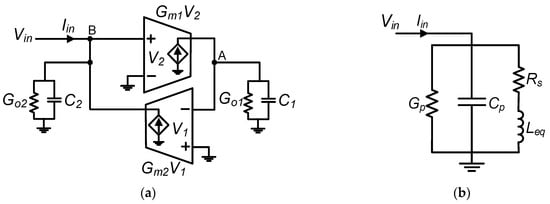
Figure 1.
Lossy (practical) single-ended gyrator-C active inductor: (a) block diagram; (b) equivalent RLC model.
In Figure 1a, Go1 and Go2 represent the output and input conductances, while C1 and C2 denote the parasitic output and input capacitances, respectively. By applying Kirchhoff’s Current Law (KCL) to nodes A and B, the input admittance measured from node B can be expressed as follows:
Referring to (1), when the output conductance (Go1) is sufficiently small and the parasitic input capacitance (C2) and input conductance (Go2) are negligible, the input impedance becomes purely inductive. However, in practical cases, the equivalent inductance introduces losses, which can be modeled as an RLC network, as illustrated in Figure 1b. Based on (1), the values of each component in the equivalent RLC circuit are determined as follows:
An important parameter that determines the maximum operating frequency of an AI is its SRF, which is denoted by ω0 and expressed as
where ωt1 and ωt2 are the cut-off frequencies of the transconductance Gm1 and Gm2, respectively, and defined by (5):
Clearly, the effectiveness of an AI design depends on identifying and minimizing parasitics. Referring to Figure 1b, the key factors mainly affecting the behavior of AI include series resistance (Rs), parallel conductance (Gp), and parallel capacitance (Cp). Furthermore, Leq and Rs can be controlled through C1 and Go1. The equations indicate that inductive bandwidth is primarily determined by the transistor’s transconductance, the parasitic capacitance Cp, and the output conductance (Go1 or gds).
2.2. Concept of Gm-Boosting
Gm-boosting is a widely adopted technique for enhancing the gain of operational amplifiers [19]. Since this technique is also utilized in the design of the proposed AI, this subsection is devoted to explaining the concept of Gm-boosting briefly, before giving the detailed analysis of the proposed AI.
In a conventional MOS transistor, the transconductance is expressed as , where is the carrier mobility (with for NMOS and for PMOS); Cox is the gate capacitance per unit area; W/L is the transistor’s aspect ratio, and ID is the bias current. Achieving a higher transconductance (gm) level typically requires a larger device size with a higher bias current, which increases power consumption and limits performance. To mitigate these drawbacks, the Gm-boosting technique has been introduced [14,15]. Figure 2 illustrates the basic principle of the Gm-boosting technique. As depicted in Figure 2b, a Gm-boosted transistor employs a feedback loop with a negative gain (). Therefore, this method enhances the transconductance by a factor, as given in (6):
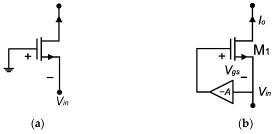
Figure 2.
Transconductance stage: (a) simple transistor; (b) Gm-boosted version.
Here, gm is the intrinsic transconductance of the MOS transistor, and A is the gain of the feedback amplifier. By incorporating a simple common-gate (CG) amplifier with a negative gain, the overall transconductance Gm is significantly increased. Regarding (6) and Figure 2, the input signal, amplified by a factor of () through the inverting gain block, is then applied to the gate of the transistor M1. As a result, the overall transconductance of the CG amplifier increases by a factor of (1 + A). It is noted that, compared with conventional designs, the feedback amplifier operates with low bias currents to achieve similar transconductance levels, ensuring minimal additional power dissipation.
This technique not only boosts the performance of the circuit by enhancing the transconductance but also reduces power consumption. As a result, these advantages make the Gm-boosting technique highly suitable for applications demanding low-power and high-performance inductive components, in RF applications, including filters, matching networks, phase shifters, and more.
2.3. Proposed Active Inductor and Its Small-Signal Characteristics
The proposed active inductor is based on a CMOS implemented gyrator-C structure, and a Gm-boosting stage connected over a feedback resistor. The schematic of the proposed AI is shown in Figure 3. The core of the gyrator-C network relies on distinct positive and negative transconductors. Specifically, transistor M3N acts as the positive transconductor (Gm1), and the regulated cascode input transistors M2N, M4N, and M5N adjust the gyrator’s negative transconductance (Gm2) block that controls the effective inductance and input parasitic capacitance independently. The control is primarily achieved through the Gm-Boosting Block (transistors M2P and M5N). In this loop, M2P and M5N function as a feedback path that drives the gate voltage of M4N. Current sources I1 and I2 are realized by MP1 and MP2, respectively. By properly varying VCTRL1 and VCTRL2, the currents through M4N and M5N are adjusted, and thus the inductance value of the AI can be tuned. Moreover, the negative resistance of the cross-coupled structure M1N, M2N helps to cancel the parasitic series resistance of the inductor, which in turn enhances the quality factor. Leveraging the Gm-boosting technique through node-4 enhances the effective transconductance of M4N, thereby improving the overall noise performance of the active inductor. Introducing the feedback resistor Rf, between core-AI and Gm-boosting stages, helps to reduce Gp and improves the quality factor. However, due to the use of the cross-coupled negative-resistance compensation and the Gm-boosting feedback loop, the circuit stability requires careful attention, especially under large tuning ranges of voltage and process and temperature variations.
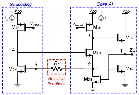
Figure 3.
Circuit diagram of proposed active inductor with resistive feedback and Gm-boosting.
In the proposed design, the bias currents I1 and I2 shown in dashed form in Figure 3 represent controllable current sources that set the operating points and tuning characteristics of the active inductor. In this implementation, these currents are generated by PMOS transistors M1P and M2P, whose values are adjusted through the gate-bias voltages VCTRL1 and VCTRL2. While simple gate-controlled current sources are used here to maintain a compact and fully integrated structure, they may be replaced by tunable current mirrors or externally controlled bias circuits. The small-signal equivalent circuit of the proposed AI is presented in Figure 4. Referring to this small-signal schematic, the input admittance of the system is calculated and given in Appendix A.
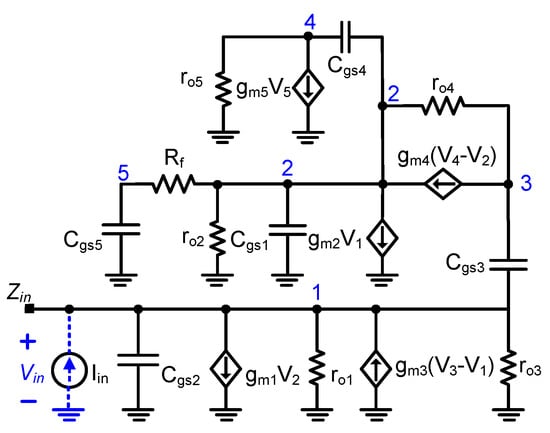
Figure 4.
Small-signal equivalent circuit of proposed active inductor.
After algebraic decomposition and simplifications, it can be modeled as an equivalent RLC circuit with the component values given in (7):
It is important to note that Leq in (7) is proportional to Rf, meaning that choosing a higher Rf leads to a higher extracted inductance. As seen from (7), the series resistance (Rs) remains unaffected by changes in Rf. The maximum frequency at which the circuit exhibits inductive behavior is referred to as the self-resonant frequency (SRF) of the active inductor and is defined as . Using the extracted expressions of Leq and Cp from (7), the SRF and quality factor of the proposed AI are obtained as in (8) and (9):
According to (8) and (9), a higher value of Rf results in an increased quality factor. This effect will also be examined through simulations in the next subsection.
2.4. Results of Proposed Active Inductor
The proposed design in Figure 3 is implemented using a 180 nm RFCMOS process with a supply voltage of 1.8 V. For reference design, circuit parameters and element values are rigorously calculated and tuned as provided in Table 2. These parameters correspond to a range of control voltages VCTRL1 and VCTRL2 varying from 600 mV to 1.2 V. VCTRL1 primarily controls the frequency band, whereas VCTRL2 has effects on the inductance values. A higher VCTRL1 results in a lower resonant frequency and vice versa. Similarly, the inductance value is proportional to VCTRL2. Variations in control voltages also affect the bias currents I1 and I2 and, consequently, the total power consumption. Since M1P and M2P are PMOS current sources, higher control voltages reduce their overdrive voltages, leading to lower power consumption.
Table 2.
Circuit parameter values.
The layout of the AI is given in Figure 5a; it occupies an area of 0.0006 mm2 (23.56 μm × 25.8 μm). As shown in Figure 5b, the inductance value varies from 4.5 nH to 215 nH by sweeping control voltages from 600 mV to 1.2 V.
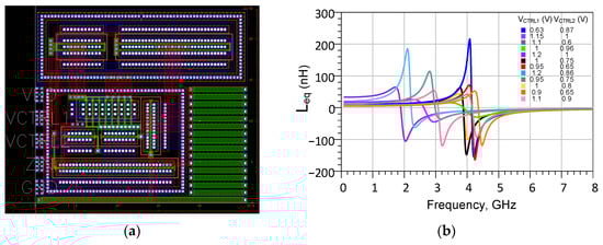
Figure 5.
Designed AI: (a) layout photograph; (b) variation of inductance versus different control voltages.
By running the simulations, the resulting performance characteristics of the AI are shown in Figure 6. The magnitude and phase of the input impedance (Zin) are depicted in Figure 6a. Examination of Figure 6a reveals that the design exhibits an inductive behavior up to 4.1 GHz. The impedance phase approaching 90° is promising for achieving a pure and high-quality inductor. As seen in Figure 6b, beyond 4.1 GHz, the imaginary part of Zin becomes negative, indicating a transition to capacitive behavior. In addition, the equivalent RLC model of the proposed AI is derived based on Figure 1b, and the approximated parameters are given as Leq = 11.78 nH, Rs = 8.21 Ω, Cp = 0.126 pF, and RP ≈ 50 kΩ. The simulated response of the RLC model is also plotted in Figure 6. A detailed comparison shows a close match between the RLC model and the designed active inductor, validating the accuracy of the equivalent representation.
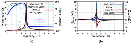
Figure 6.
Simulated input impedance (Zin) of the proposed AI: (a) magnitude and phase; (b) real and imaginary parts.
In the proposed active inductor, a feedback resistor Rf is intentionally inserted between the core gyrator-C structure and the Gm-boosting stage to regulate the boosting loop and enhance the overall performance. The resistor Rf provides a controlled feedback path that limits the loop gain, stabilizes the boosted transconductance, and reduces the equivalent parallel loss Gp. As demonstrated by the analytical expressions in (7), the extracted inductance Leq increases proportionally with Rf. Moreover, substituting Leq and Cp into (8) and (9) shows that a larger Rf directly leads to a higher quality factor. As predicted by (7)–(9), an increase in the value of Rf yields an improved quality factor. This relationship is illustrated in Figure 7a,b, which shows the quality factor for various values of Rf. As shown in the figure, the quality factor reaches values around 1000 and can rise as high as 5000. The high quality factor observed in Figure 7 arises from the combined effect of the negative-resistance compensation provided by the cross-coupled pair (M1N, M2N) and the substantial enhancement of the effective transconductance generated by the Gm-boosting loop around M4N. In the proposed gyrator-C active inductor, the equivalent series resistance Rs becomes very small when the negative conductance introduced by the cross-coupled devices nearly cancels the parasitic channel and bias-dependent resistances of the core transconductance stage. At the same time, the feedback-assisted Gm-boosting path (M2P, M5N), together with the feedback resistor Rf, increases the effective gm4 while reducing the parallel conductance Gp, thereby raising the equivalent parallel resistance (Rp ≈ 1/Gp). Nonetheless, we acknowledge that parasitic effects, device mismatch, and practical implementation constraints tend to reduce the achievable Q. To observe the noise performance of the circuit, the simulated input-referred current noise is presented in Figure 7c. The input-referred noise at maximum quality factor (i.e., at 2.7 GHz) is as depicted in the figure.
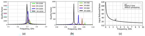
Figure 7.
Simulation results of the proposed AI: (a) effect of Rf variation on quality factor at lower frequency; (b) effect of Rf variation on quality factor at higher frequency; (c) input referred noise.
To evaluate the stability of the proposed active inductor, two separate loop-gain analyses were performed. The first loop is formed by the feedback resistor Rf, and its loop gain was obtained by breaking the path across Rf and measuring the corresponding response. The second loop corresponds to the Gm-boosting path, for which the loop gain was similarly extracted by breaking the internal boosting loop. Loop-gain curves were generated for various control-voltage settings for both loops. For lower control voltage values, all the loop gains remain below unity, indicating a stable operating region. For the cases in which the loop gain exceeds unity, the corresponding magnitude and phase responses are plotted in Figure 8 and Figure 9, for the Rf path and the Gm-boosting path, respectively. An examination of Figure 8b and Figure 9b shows that the phase margins remain well above commonly accepted stability limits, all exceeding 45°. Based on the simulations, it can be observed that the proposed active inductor remains stabilized for VCTRL values below 1.2 V, while instability may begin to appear above this level due to excessive boosting. This analysis indicates that the proposed active inductor exhibits stable behavior across typical operating conditions for the component values used.
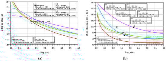
Figure 8.
Loop gain results of the proposed AI over Rf path: (a) magnitude; (b) phase.
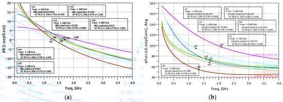
Figure 9.
Loop gain results of the proposed AI over Gm-boosting path: (a) magnitude; (b) phase.
In order to assess the robustness of the proposed active inductor under practical operating conditions, corner, temperature, and Monte Carlo analyses were performed. These analyses collectively assess the sensitivity of the design to process variations, thermal changes, and device mismatch. In MOSFETs, process parameters such as oxide thickness, doping concentration, and threshold voltage fluctuate, causing deviations from nominal values. As a result, the current can vary, being higher at the Fast Corner or lower at the Slow Corner, depending on the fluctuations in each parameter. When designing a circuit, the designer must ensure that the circuit is compatible with these process variations. In this study, three corner models from the RFCMOS 0.18 μm model library were utilized: TT (Typical–Typical), FF (Fast–Fast), and SS (Slow–Slow), representing the typical, fast, and slow process variations, respectively. Corner analyses, as depicted in Figure 10a,b, show a slight variation in the obtained value for the concerned corner. As expected, different corner sections result in noticeable variations in performance, without altering the overall behavior of the circuit. An analog circuit can be subjected to temperature variations, so temperature sweep analyses were performed for the imaginary part of the input impedance and the equivalent inductance, as depicted in Figure 11a,b.
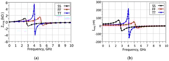
Figure 10.
Corner analysis for the proposed AI: (a) imaginary part of input impedance; (b) equivalent inductance.
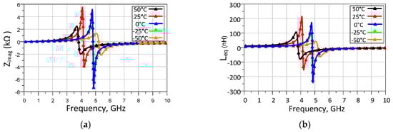
Figure 11.
Temperature effect on AI: (a) imaginary part of input impedance; (b) equivalent inductance.
The Monte Carlo analysis can be used to examine process variation and device mismatch of a circuit and study its impact on the design. Therefore, it allows us to examine and predict circuit performance variations, which may affect yield. Monte Carlo analysis with a sample size of 1000 was performed by applying Gaussian distribution with three sigma variations. Figure 12a,b show the statistical distribution of simulated parameters with respect to histograms. It can be illustrated from the figures that the simulated parameters have low standard deviations from their mean values.
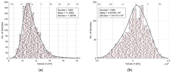
Figure 12.
Monte Carlo simulation-based histogram of the AI: (a) equivalent inductance; (b) SRF.
Finally, the overall performance of the proposed AI is summarized in Table 3 with comparisons to other existing similar studies, highlighting its superior performance.
Table 3.
Performance comparison table.
3. Application of the Proposed AI in a Broadband RF Amplifier Design
In this section, we present a demonstration of the proposed AI structure in a microwave amplifier system. Specifically, we aim to design a broadband small-signal RF amplifier using CMOS technology operating within the 0.8–2.1 GHz frequency band, intended for sub-6 GHz 5G and beyond wireless communication systems. To achieve this, we used a common-source transistor with the following parameters: width W = 400 μm and length L = 180 nm, biased with VDC = 1.8 V drain voltage and VGG = 0.65 V gate voltage applied over RF chokes. Additionally, a feedback resistor RFB was inserted between the drain and gate terminals of the transistor to improve stability, accompanied by a feedback capacitor CFB to block DC leakage within the feedback path. To further improve the stability, a small-valued series RO in resistance is also included at the drain end of the transistor.
Under these fixed conditions, we measured the S-parameters of the biased and stabilized transistor. These measured S-parameters were then used to design the appropriate matching networks for 50 Ω source and load terminations, which is a standard for microwave applications. In the design process, the transducer power gain (TPG) of the system was optimized using the Simplified Real Frequency Technique (SRFT). It is noted that SRFT is a robust numerical method for designing broadband microwave amplifiers, as it directly utilizes the transistor’s S-parameters rather than requiring impedance or admittance representations [24,25,26,27]. For the selected target minimum gain level T0 = 14 dB, both the input matching network (IMN) and the output matching network (OMN) were synthesized with ideal circuit components. The final schematic of the designed amplifier is shown in Figure 13. Evaluation of Figure 13 indicates that the inductor Lo2, with a value of 9 nH in the OMN, is well suited for integration with our proposed AI circuit, as it is connected in shunt with the signal path. To validate the AI design, we replaced Lo2 with the proposed AI, carefully tuning its parameters to closely approximate the target inductance value. Additionally, an equivalent RLC model of the designed AI was extracted with the element values of Leq = 9.5 nH, Rs = 0.5 Ω, Cp = 0.25 pF, and RP ≈ 1 kΩ. The corresponding simulation results are presented in Figure 14 and Figure 15.
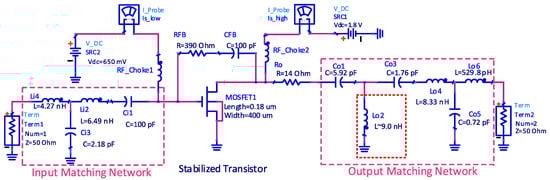
Figure 13.
Designed broadband RF amplifier and usage of the proposed AI at the OMN to realize shunt inductor Lo2.
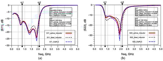
Figure 14.
Performance results of the designed amplifier: (a) input reflection; (b) output reflection.
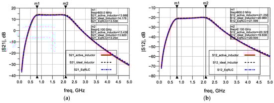
Figure 15.
Performance results of the designed amplifier: (a) gain |S21|; (b) isolation |S12|.
Figure 14a,b show the input and output reflectance results of the amplifier, respectively. In both cases (ideal inductor and AI), |S11| and |S22| remain below −10 dB over the frequency band of operation. Analysis of the figures reveals that input and output reflection performances are close to each other along the band of operation. In Figure 15a, the TPG of the amplifier for both the ideal inductor and AI cases are presented. As shown from the figure, the performance with the AI is nearly identical to the ideal case, with a gain ranging from 13.43 dB to 13.88 dB, exhibiting only a minimal and negligible decrease compared with the ideal case. The |S12| performance results given in Figure 15b show that the active inductor and the ideal model are in good agreement, with S12 reaching approximately −20 dB, indicating a fine isolation performance within the frequency band of interest. Figure 16a presents the noise figure (NF) performances of the amplifier for both AI and ideal inductor cases. From the figure, it is observed that, while there is an increase of about 1.48 dB at the lower cut-off frequency (reaching 5.48 dB level at 0.8 GHz), the noise figure for the AI case approaches the ideal inductor performance as frequency increases, becoming 3.43 dB at 2.1 GHz. This demonstrates that the proposed AI exhibits low noise figure performance, comparable to the ideal case. In this design, the active inductor Lo2 creates a transmission zero at DC and maintains the lower cut-off slope. At low frequencies, Lo2 acts as a short circuit, while at higher RF frequencies (up to 2.1 GHz), its impedance increases toward an open circuit, shunting the noise current away from the signal path. Consequently, the active inductor’s noise contribution becomes negligible at the operating frequency, explaining the noise figure behavior observed in Figure 16. The stability analysis of the amplifier incorporating the active inductor Lo2 was performed together with a Monte Carlo analysis that includes statistical, mismatch, and process variations. The resulting plotted Rollett stability factor (K), μ-factor (load), and μ-factor (source) are presented in Figure 16b and Figure 17a,b, respectively, along with their nominal values (red curves) and Monte Carlo variations (gray curves). As seen from the figures, the K-factor and μ-factors remain above unity with sufficient margins, indicating stable operation over the entire frequency band. Through this example, it is shown that the proposed AI can be effectively used in RFIC systems, specifically in matching networks, to replace passive inductors, making it a promising and efficient technology for 5G and future communication systems.
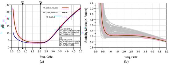
Figure 16.
Performance results of the amplifier: (a) noise figure; (b) stability metric [K] with Monte Carlo analysis.
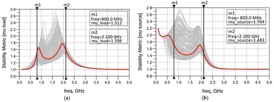
Figure 17.
Stability metrics with Monte Carlo simulations: (a) μ-load; (b) μ-source.
4. Conclusions
A novel low-power, high-quality factor, wide-tunable, and broadband CMOS active inductor based on a gyrator-C configuration is presented. Through the application of the Gm-boosting technique, the AI achieves significant improvements in both performance and power efficiency, while a feedback resistor further boosts the quality factor. The inductance can be tuned ranging from 4.5 nH to 215 nH, across a wide frequency range up to 4.1 GHz, with a power consumption of only 1.82 mW at a 1.8 V supply, and the AI exhibits a low input-referred current noise as , making it ideal for low-noise applications. The compactness of the design, with a chip area of 0.0006 mm2, makes it a strong candidate for integration in RF systems.
The versatility of the proposed AI was demonstrated by incorporating it into a broadband RF amplifier design for RFIC applications, which operates within a 0.8–2.1 GHz bandwidth and provides near-ideal performance. The results validate the potential of the proposed AI for meeting the stringent demands of modern wireless GSM and 5G and beyond communication systems. The robustness and reliability of the proposed design are validated by performing temperature, stability, corner, and Monte Carlo analyses. In conclusion, the proposed AI offers an advantageous solution for future wireless communication systems, providing a compact and efficient inductive component that can be integrated into complex RF circuits.
Author Contributions
Conceptualization, S.K. and F.K.; methodology, M.K. and S.K.; formal analysis, M.A.O. and M.K.; validation, M.K.; writing—original draft preparation, M.K.; writing—review and editing, S.K. and M.A.O.; visualization, M.A.O.; supervision, F.K. All authors have read and agreed to the published version of the manuscript.
Funding
This research received no external funding.
Data Availability Statement
Data are contained within the article.
Acknowledgments
This research incorporates the outcomes, methodologies, and technical experience gained from the research project No. 124E300 of the Scientific and Technological Research Council of Türkiye (TUBITAK), which contributed to the development of the proposed design. The authors gratefully acknowledge TUBITAK for its support.
Conflicts of Interest
Author Merve Kilinc was employed by the company ULAK HABERLEŞME A.Ş. The remaining authors declare that the research was conducted in the absence of any commercial or financial relationships that could be construed as potential conflicts of interest.
Appendix A
Applying KCL to nodes 1, 2, 3, 4, and 5 in Figure 4, respectively, gives (A1)–(A5):
in which is equal to and is equal to .
Solving this system of equations, the input admittance (Yin) of the proposed AI is derived by substituting V2, V3, V4, and V5 from (A2)–(A5) to (A1) as follows:
References
- Long, J.R. Passive components for silicon RF and MMIC design. IEICE Trans. Electron. 2003, 86, 1022–1031. [Google Scholar]
- Liu, B.; Zhao, D.; Reynaert, P.; Gielen, G.G. Synthesis of integrated passive components for high-frequency RF ICs based on evolutionary computation and machine learning techniques. IEEE Trans. Comput.-Aided Des. Integr. Circuits Syst. 2011, 30, 1458–1468. [Google Scholar] [CrossRef]
- Yoon, Y.; Kim, J.; Kim, H.; An, K.H.; Lee, O.; Lee, C.H.; Kenney, J.S. A dual-mode CMOS RF power amplifier with integrated tunable matching network. IEEE Trans. Microw. Theory Tech. 2011, 60, 77–88. [Google Scholar] [CrossRef]
- Shaeffer, D.K.; Lee, T.H. A 1.5-V, 1.5-GHz CMOS low noise amplifier. IEEE J. Solid-State Circuits 2002, 32, 745–759. [Google Scholar] [CrossRef]
- Long, J.R.; Copeland, M.A. The modeling, characterization, and design of monolithic inductors for silicon RF IC’s. IEEE J. Solid-State Circuits 2002, 32, 357–369. [Google Scholar] [CrossRef]
- Tang, X.; Mouthaan, K. Design of large bandwidth phase shifters using common mode all-pass networks. IEEE Microw. Wirel. Compon. Lett. 2012, 22, 55–57. [Google Scholar] [CrossRef]
- Mariappan, S.; Rajendran, J.; Idros, N.; Manaf, A.A.; Kumar, N.; Alghaihab, A.; Yarman, B.S. A review of engineering techniques for CMOS on-chip inductor design and quality factor enhancement from MHz-to-GHz frequency domains. IEEE Access 2025, 13, 140473–140499. [Google Scholar] [CrossRef]
- Yuan, F. CMOS Active Inductors and Transformers, 1st ed.; Springer: Boston, MA, USA, 2008; pp. 21–99. [Google Scholar]
- Hsiao, C.C.; Kuo, C.W.; Ho, C.C.; Chan, Y.J. Improved quality-factor of 0.18-μm CMOS active inductor by a feedback resistance design. IEEE Microw. Wirel. Compon. Lett. 2002, 12, 467–469. [Google Scholar] [CrossRef]
- Torres, J.A.; Freire, J.C. K Band SiGe HBT single ended active inductors. Integration 2016, 52, 272–281. [Google Scholar] [CrossRef]
- Zito, D.; Pepe, D.; Fonte, A. High-frequency CMOS active inductor: Design methodology and noise analysis. IEEE Trans. Very Large Scale Integr. (VLSI) Syst. 2014, 23, 1123–1136. [Google Scholar] [CrossRef]
- Konal, M.; Kacar, F. MOS only grounded active inductor circuits and their filter applications. J. Circuits Syst. Comput. 2017, 26, 1750098. [Google Scholar] [CrossRef]
- Hota, A.K.; Sethi, K. 2.4 GHz active inductor based single to differential LNA for WLAN applications. IETE J. Res. 2024, 70, 4011–4024. [Google Scholar] [CrossRef]
- Li, X.; Shekhar, S.; Allstot, D.J. G/sub m/-boosted common-gate LNA and differential colpitts VCO/QVCO in 0.18-/spl mu/m CMOS. IEEE J. Solid-State Circuits 2005, 40, 2609–2619. [Google Scholar]
- Sabbaghi, A.; Ebrahimi, E. A low-noise current-reused CMOS active inductor by exploiting Gm-boosting technique. IET Microw. Antennas Propag. 2021, 15, 1914–1926. [Google Scholar] [CrossRef]
- Mhiri, M.; Besbes, K. Gyrator-C-based CMOS active inductors: Analysis of performance optimization techniques. IEEE Microw. Mag. 2021, 22, 65–82. [Google Scholar] [CrossRef]
- Yuan, F. CMOS gyrator-C active transformers. IET Circuits Devices Syst. 2007, 1, 494–508. [Google Scholar] [CrossRef]
- Bansal, U.; Garg, A.; Shalini, D. A review on recently reported grounded CMOS active inductors. Wirel. Pers. Commun. 2023, 133, 913–949. [Google Scholar] [CrossRef]
- Chiou, H.K.; Chen, S.C. Low phase noise Ku-band Gm-boosting differential Colpitts VCO. In Proceedings of the 2009 Asia Pacific Microwave Conference, Singapore, 7–10 December 2009; pp. 313–316. [Google Scholar]
- Saad, S.; Ben Hammadi, A.; Haddad, F. Design and realization of a high-Q grounded tunable active inductor for 5G NR (FR1) transceiver front-end applications. Sensors 2025, 25, 3070. [Google Scholar] [CrossRef] [PubMed]
- Kizmaz, M.M.; Herencsar, N.; Cicekoglu, O. Wide-tunable LC-VCO design with a novel active inductor. AEU-Int. J. Electron. Commun. 2022, 153, 154266. [Google Scholar] [CrossRef]
- Gurjar, R.C.; Mishra, D.K. Design and performance analysis of CMOS tunable active inductor based voltage controlled oscillator. Int. J. Electron. 2022, 109, 915–934. [Google Scholar] [CrossRef]
- Sachan, D.; Goswami, M.; Misra, P.K. Design of ultra-low power high-Q single ended active inductors for IF BPF of receiver frontend using 130 nm BiCMOS technology. Wirel. Pers. Commun. 2021, 120, 649–663. [Google Scholar] [CrossRef]
- Yarman, B.S. Design of Ultra Wideband Power Transfer Networks, 1st ed.; John Wiley & Sons: New York, NY, USA, 2010. [Google Scholar]
- Yarman, B.S.; Carlin, H.J. A simplified “real frequency” technique applied to broad-band multistage microwave amplifiers. IEEE Trans. Microw. Theory Tech. 1982, 30, 2216–2222. [Google Scholar] [CrossRef]
- Kilinc, S.; Ormanci, M.A.; Yildirim, A.; Kizilbey, O.; Yarman, B.S. An SRFT Tool to Design Broadband Microwave Amplifiers for Complex Impedance Conditions. In Proceedings of the 2024 IEEE INC-USNC-URSI Radio Science Meeting (Joint with AP-S Symposium), Florence, Italy, 14–19 July 2024; pp. 99–100. [Google Scholar]
- Kilinc, S.; Ormanci, M.A.; Yarman, B.S. An SRFT Tool to Design Broadband Microwave Amplifiers with Customized Objective Functions. In Proceedings of the 2023 30th IEEE International Conference on Electronics, Circuits and Systems (ICECS), Istanbul, Türkiye, 4–7 December 2023; pp. 1–4. [Google Scholar]
Disclaimer/Publisher’s Note: The statements, opinions and data contained in all publications are solely those of the individual author(s) and contributor(s) and not of MDPI and/or the editor(s). MDPI and/or the editor(s) disclaim responsibility for any injury to people or property resulting from any ideas, methods, instructions or products referred to in the content. |
© 2025 by the authors. Licensee MDPI, Basel, Switzerland. This article is an open access article distributed under the terms and conditions of the Creative Commons Attribution (CC BY) license (https://creativecommons.org/licenses/by/4.0/).