CMOS Active Inductor Using Gm-Boosting Technique with Resistive Feedback and Its Broadband RF Application
Abstract
1. Introduction
2. Proposed Active Inductor: Concept and Design
2.1. Basic Principles of Active Inductors
2.2. Concept of Gm-Boosting
2.3. Proposed Active Inductor and Its Small-Signal Characteristics
2.4. Results of Proposed Active Inductor
3. Application of the Proposed AI in a Broadband RF Amplifier Design
4. Conclusions
Author Contributions
Funding
Data Availability Statement
Acknowledgments
Conflicts of Interest
Appendix A
References
- Long, J.R. Passive components for silicon RF and MMIC design. IEICE Trans. Electron. 2003, 86, 1022–1031. [Google Scholar]
- Liu, B.; Zhao, D.; Reynaert, P.; Gielen, G.G. Synthesis of integrated passive components for high-frequency RF ICs based on evolutionary computation and machine learning techniques. IEEE Trans. Comput.-Aided Des. Integr. Circuits Syst. 2011, 30, 1458–1468. [Google Scholar] [CrossRef]
- Yoon, Y.; Kim, J.; Kim, H.; An, K.H.; Lee, O.; Lee, C.H.; Kenney, J.S. A dual-mode CMOS RF power amplifier with integrated tunable matching network. IEEE Trans. Microw. Theory Tech. 2011, 60, 77–88. [Google Scholar] [CrossRef]
- Shaeffer, D.K.; Lee, T.H. A 1.5-V, 1.5-GHz CMOS low noise amplifier. IEEE J. Solid-State Circuits 2002, 32, 745–759. [Google Scholar] [CrossRef]
- Long, J.R.; Copeland, M.A. The modeling, characterization, and design of monolithic inductors for silicon RF IC’s. IEEE J. Solid-State Circuits 2002, 32, 357–369. [Google Scholar] [CrossRef]
- Tang, X.; Mouthaan, K. Design of large bandwidth phase shifters using common mode all-pass networks. IEEE Microw. Wirel. Compon. Lett. 2012, 22, 55–57. [Google Scholar] [CrossRef]
- Mariappan, S.; Rajendran, J.; Idros, N.; Manaf, A.A.; Kumar, N.; Alghaihab, A.; Yarman, B.S. A review of engineering techniques for CMOS on-chip inductor design and quality factor enhancement from MHz-to-GHz frequency domains. IEEE Access 2025, 13, 140473–140499. [Google Scholar] [CrossRef]
- Yuan, F. CMOS Active Inductors and Transformers, 1st ed.; Springer: Boston, MA, USA, 2008; pp. 21–99. [Google Scholar]
- Hsiao, C.C.; Kuo, C.W.; Ho, C.C.; Chan, Y.J. Improved quality-factor of 0.18-μm CMOS active inductor by a feedback resistance design. IEEE Microw. Wirel. Compon. Lett. 2002, 12, 467–469. [Google Scholar] [CrossRef]
- Torres, J.A.; Freire, J.C. K Band SiGe HBT single ended active inductors. Integration 2016, 52, 272–281. [Google Scholar] [CrossRef]
- Zito, D.; Pepe, D.; Fonte, A. High-frequency CMOS active inductor: Design methodology and noise analysis. IEEE Trans. Very Large Scale Integr. (VLSI) Syst. 2014, 23, 1123–1136. [Google Scholar] [CrossRef]
- Konal, M.; Kacar, F. MOS only grounded active inductor circuits and their filter applications. J. Circuits Syst. Comput. 2017, 26, 1750098. [Google Scholar] [CrossRef]
- Hota, A.K.; Sethi, K. 2.4 GHz active inductor based single to differential LNA for WLAN applications. IETE J. Res. 2024, 70, 4011–4024. [Google Scholar] [CrossRef]
- Li, X.; Shekhar, S.; Allstot, D.J. G/sub m/-boosted common-gate LNA and differential colpitts VCO/QVCO in 0.18-/spl mu/m CMOS. IEEE J. Solid-State Circuits 2005, 40, 2609–2619. [Google Scholar]
- Sabbaghi, A.; Ebrahimi, E. A low-noise current-reused CMOS active inductor by exploiting Gm-boosting technique. IET Microw. Antennas Propag. 2021, 15, 1914–1926. [Google Scholar] [CrossRef]
- Mhiri, M.; Besbes, K. Gyrator-C-based CMOS active inductors: Analysis of performance optimization techniques. IEEE Microw. Mag. 2021, 22, 65–82. [Google Scholar] [CrossRef]
- Yuan, F. CMOS gyrator-C active transformers. IET Circuits Devices Syst. 2007, 1, 494–508. [Google Scholar] [CrossRef]
- Bansal, U.; Garg, A.; Shalini, D. A review on recently reported grounded CMOS active inductors. Wirel. Pers. Commun. 2023, 133, 913–949. [Google Scholar] [CrossRef]
- Chiou, H.K.; Chen, S.C. Low phase noise Ku-band Gm-boosting differential Colpitts VCO. In Proceedings of the 2009 Asia Pacific Microwave Conference, Singapore, 7–10 December 2009; pp. 313–316. [Google Scholar]
- Saad, S.; Ben Hammadi, A.; Haddad, F. Design and realization of a high-Q grounded tunable active inductor for 5G NR (FR1) transceiver front-end applications. Sensors 2025, 25, 3070. [Google Scholar] [CrossRef] [PubMed]
- Kizmaz, M.M.; Herencsar, N.; Cicekoglu, O. Wide-tunable LC-VCO design with a novel active inductor. AEU-Int. J. Electron. Commun. 2022, 153, 154266. [Google Scholar] [CrossRef]
- Gurjar, R.C.; Mishra, D.K. Design and performance analysis of CMOS tunable active inductor based voltage controlled oscillator. Int. J. Electron. 2022, 109, 915–934. [Google Scholar] [CrossRef]
- Sachan, D.; Goswami, M.; Misra, P.K. Design of ultra-low power high-Q single ended active inductors for IF BPF of receiver frontend using 130 nm BiCMOS technology. Wirel. Pers. Commun. 2021, 120, 649–663. [Google Scholar] [CrossRef]
- Yarman, B.S. Design of Ultra Wideband Power Transfer Networks, 1st ed.; John Wiley & Sons: New York, NY, USA, 2010. [Google Scholar]
- Yarman, B.S.; Carlin, H.J. A simplified “real frequency” technique applied to broad-band multistage microwave amplifiers. IEEE Trans. Microw. Theory Tech. 1982, 30, 2216–2222. [Google Scholar] [CrossRef]
- Kilinc, S.; Ormanci, M.A.; Yildirim, A.; Kizilbey, O.; Yarman, B.S. An SRFT Tool to Design Broadband Microwave Amplifiers for Complex Impedance Conditions. In Proceedings of the 2024 IEEE INC-USNC-URSI Radio Science Meeting (Joint with AP-S Symposium), Florence, Italy, 14–19 July 2024; pp. 99–100. [Google Scholar]
- Kilinc, S.; Ormanci, M.A.; Yarman, B.S. An SRFT Tool to Design Broadband Microwave Amplifiers with Customized Objective Functions. In Proceedings of the 2023 30th IEEE International Conference on Electronics, Circuits and Systems (ICECS), Istanbul, Türkiye, 4–7 December 2023; pp. 1–4. [Google Scholar]
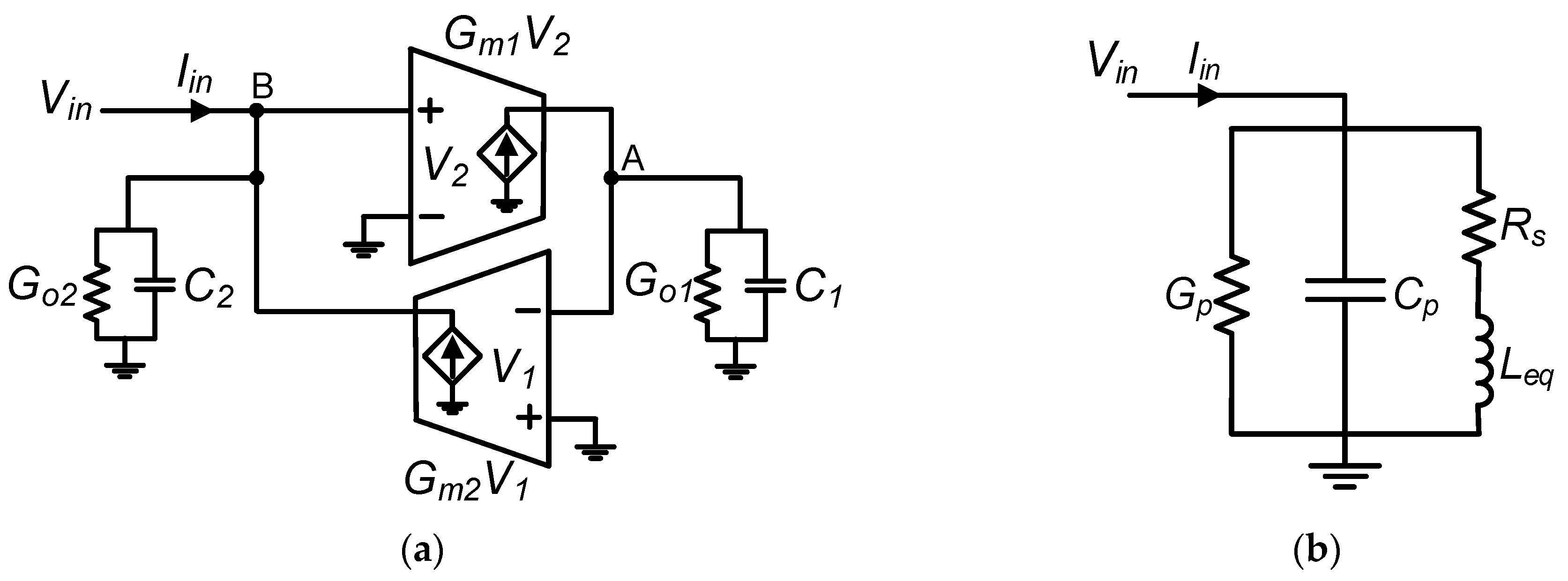
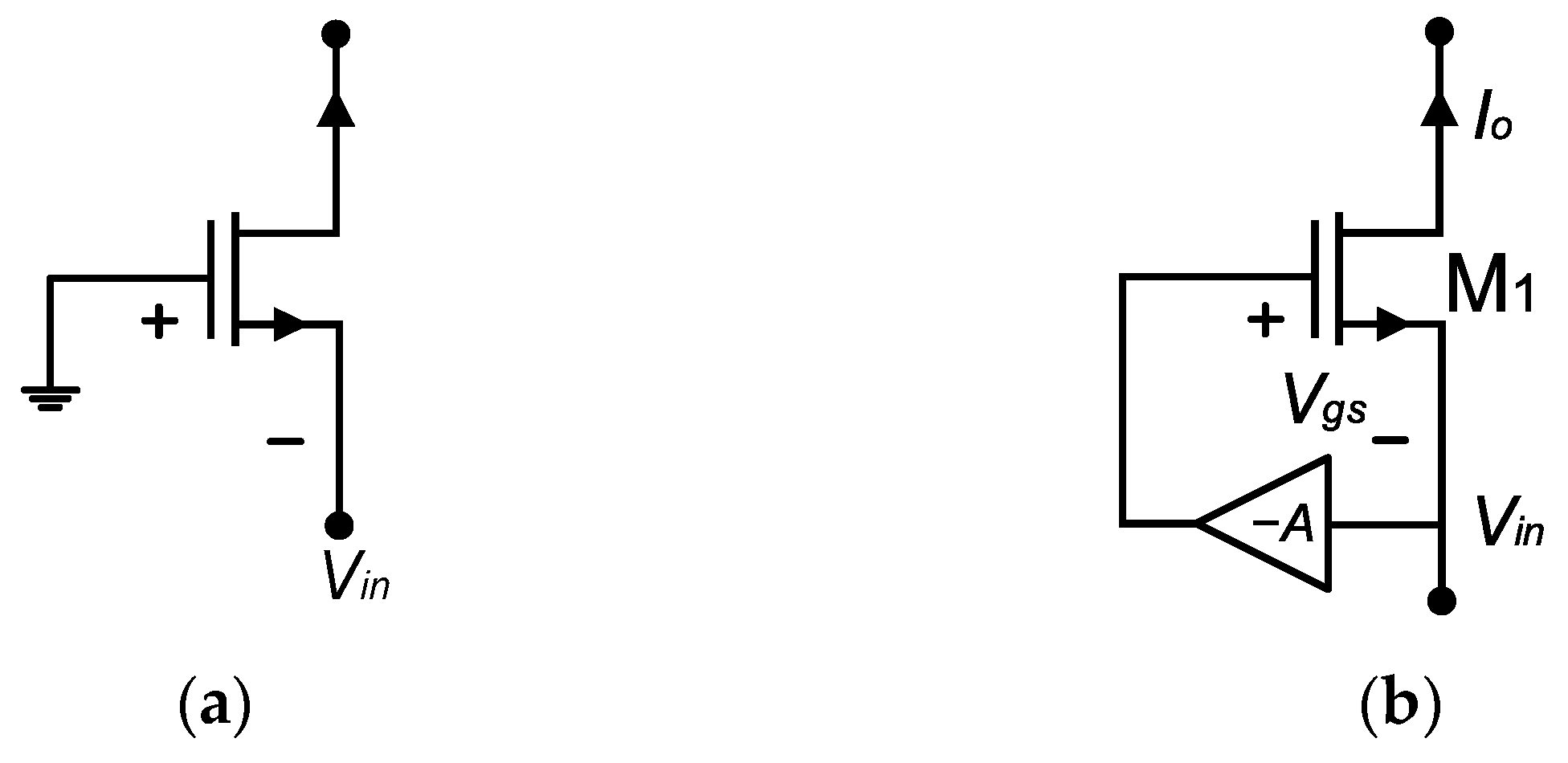
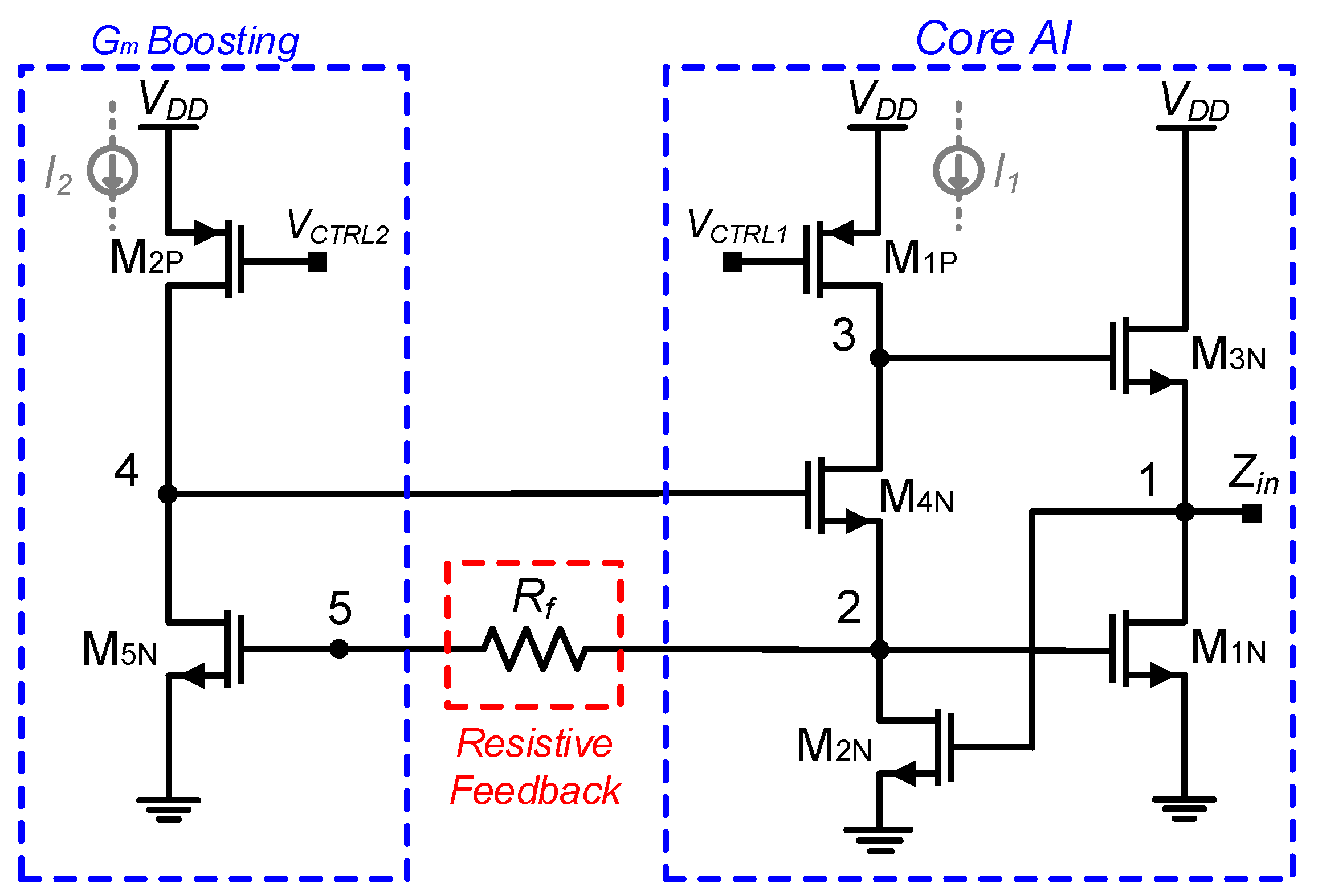
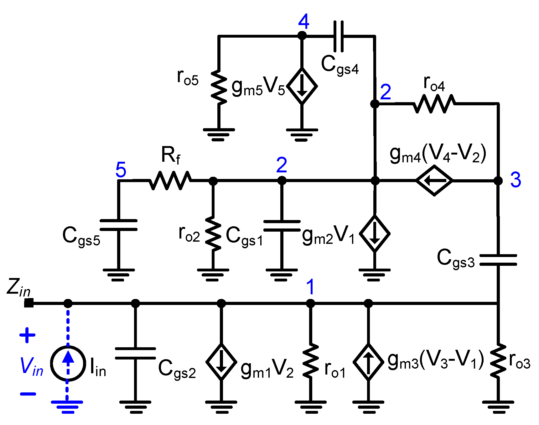
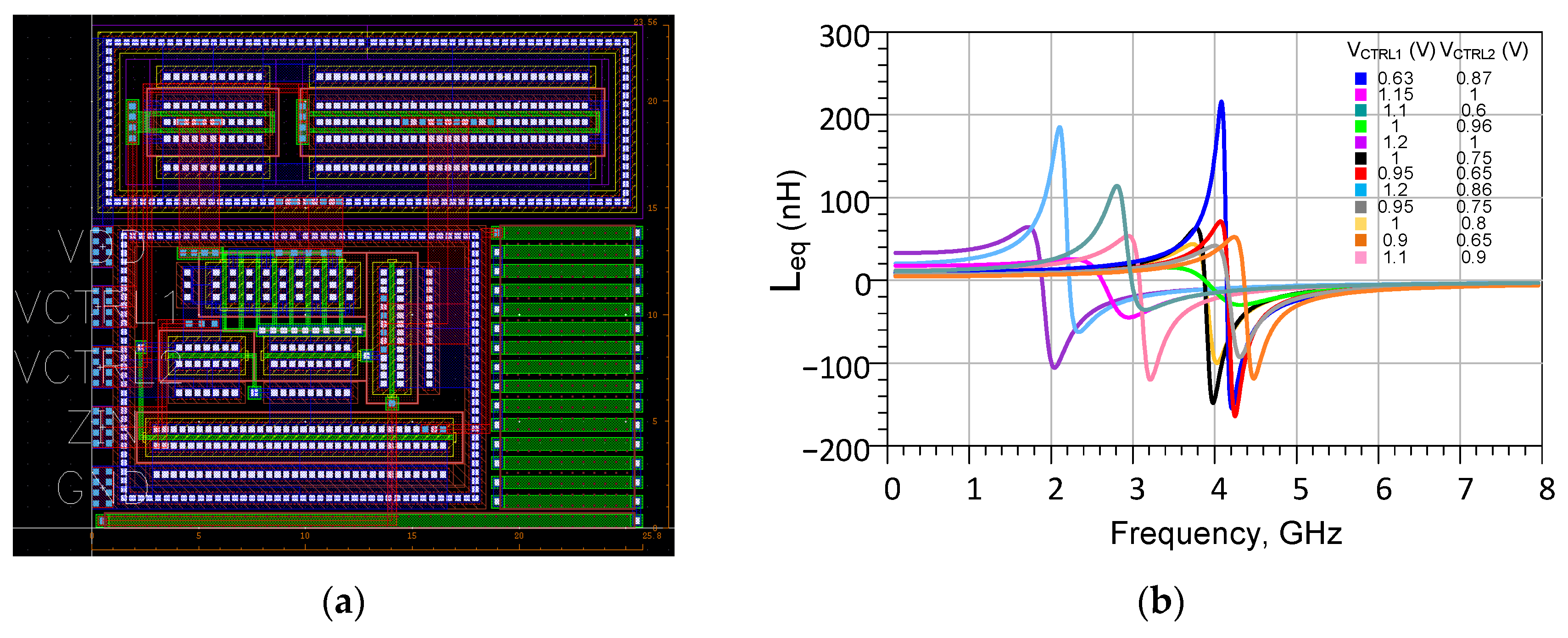
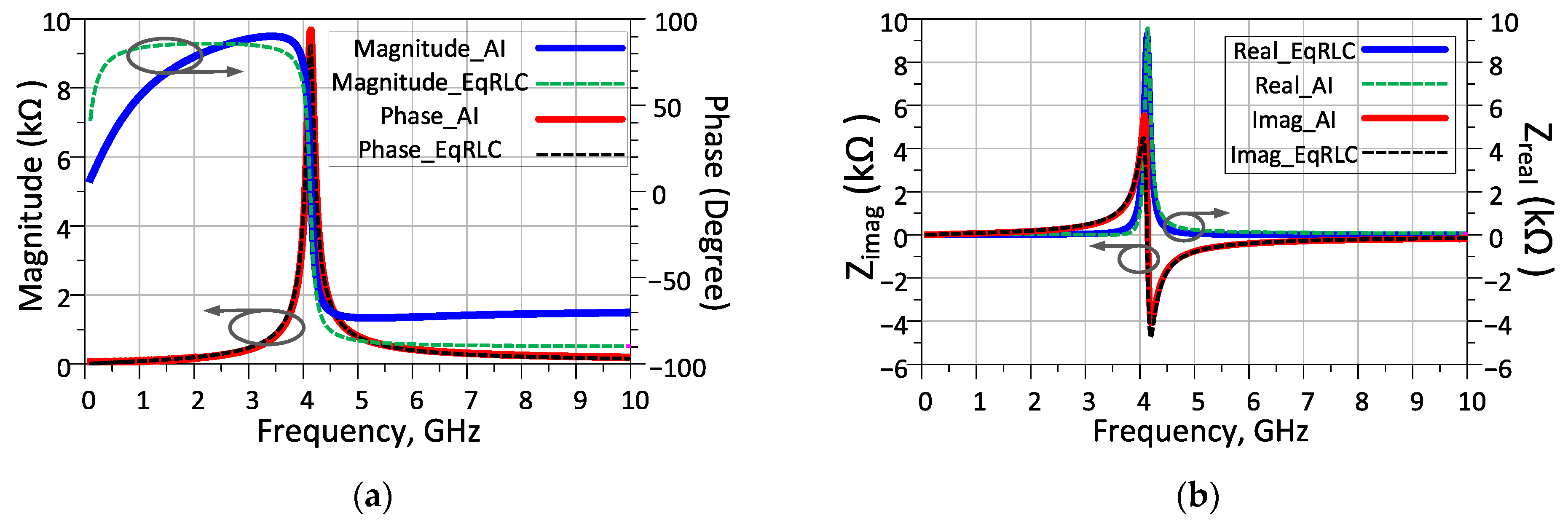

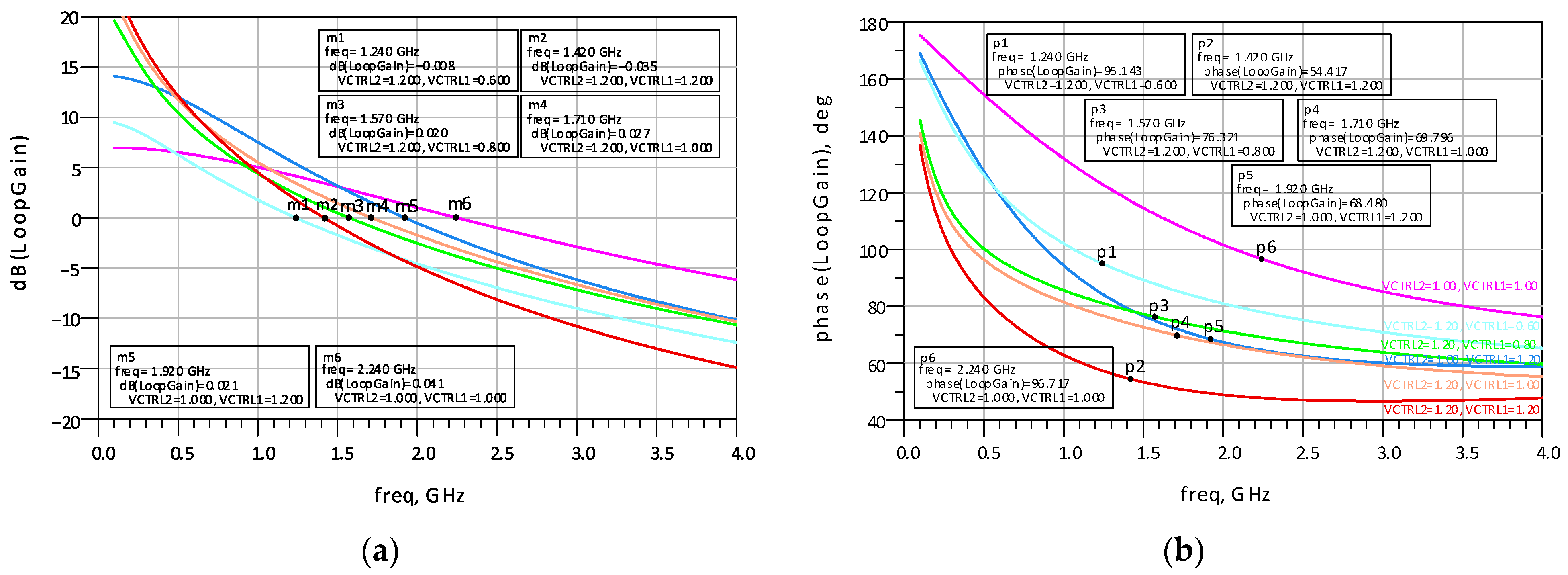
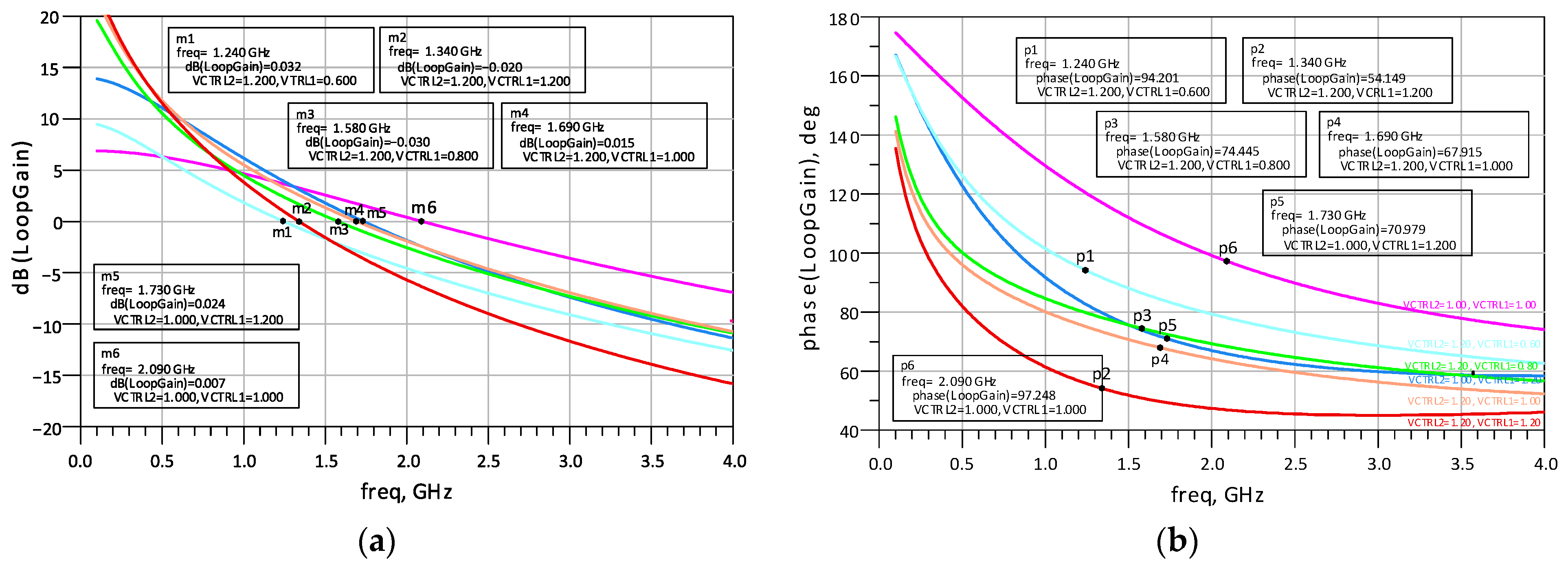
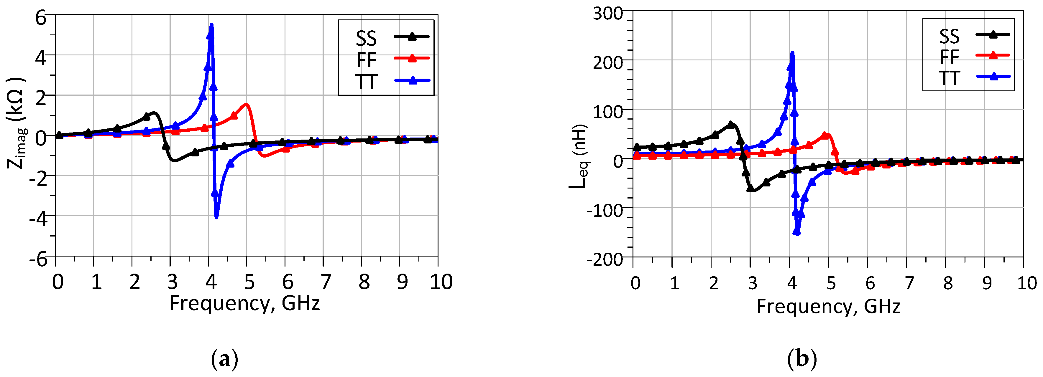
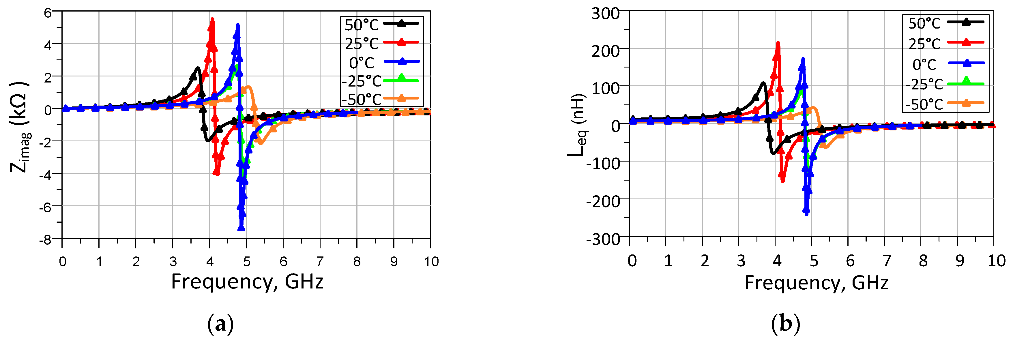
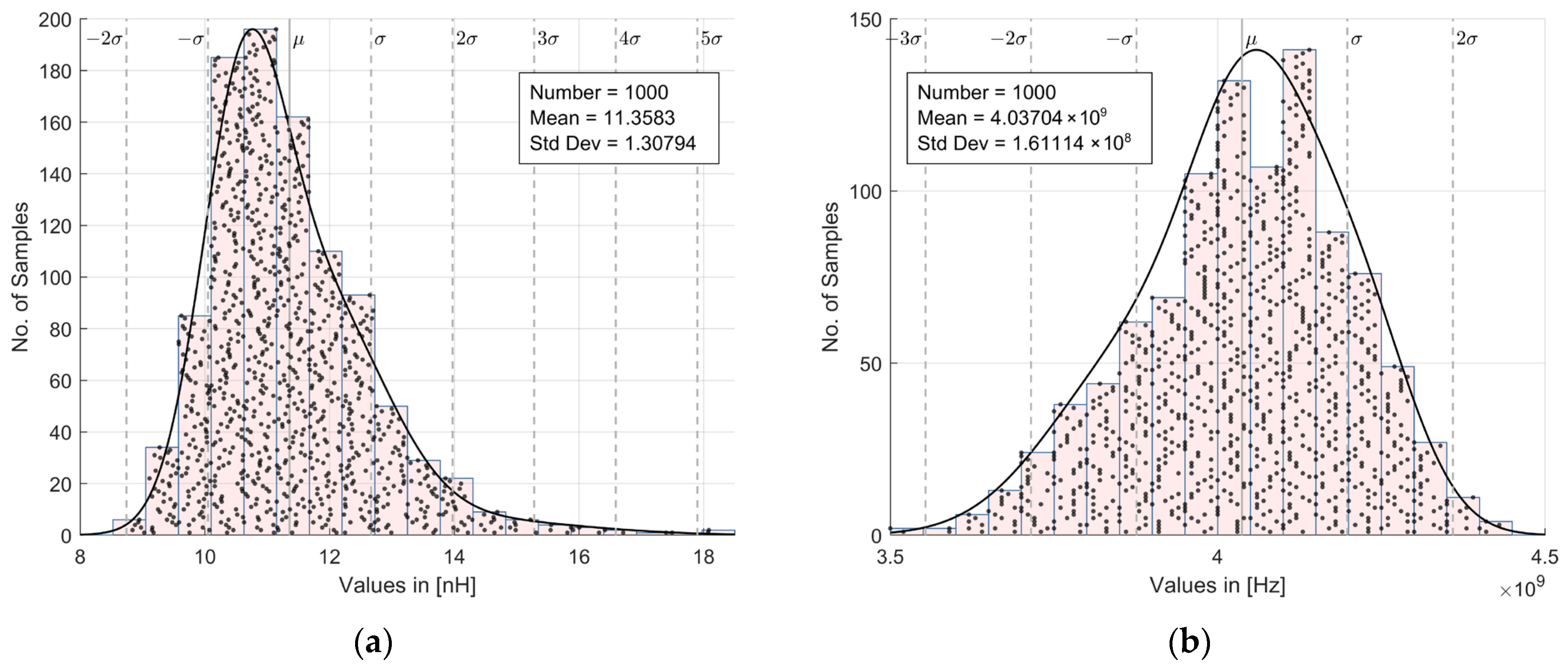

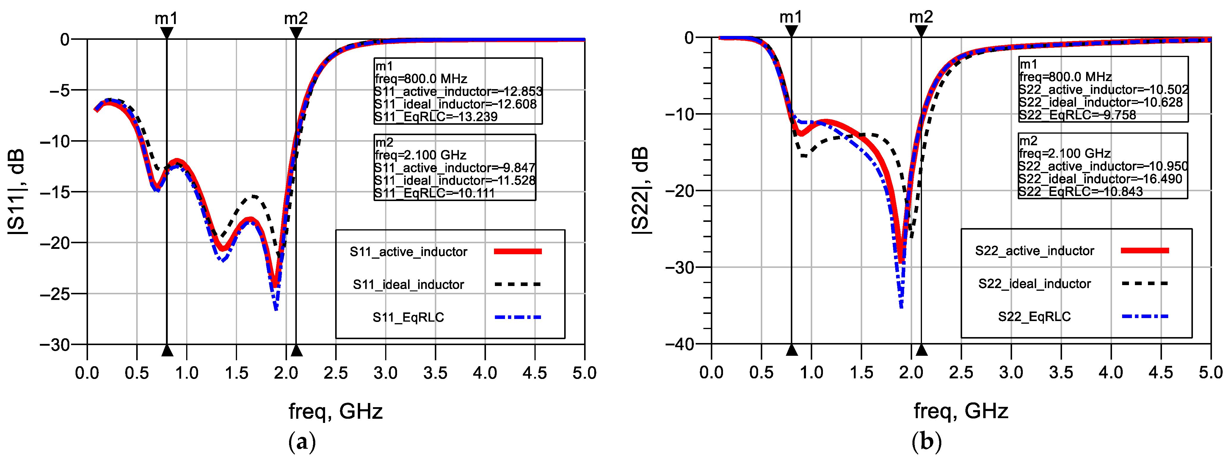
| Parameter | Active Inductors | Passive Inductors |
|---|---|---|
| Main difference | Realized using active elements like transistors and capacitors | Uses metal traces (spirals) or off-chip coils on silicon substrate |
| Size and integration | Area is small, suitable for high-density ICs, and decreases when transistor gate width decreases | Occupied area is large and increases when inductance increases |
| Linearity | Signal distortion when operating in large-signal regime | Superior linearity |
| Quality factor | High quality factor | Low quality factor |
| Tunability | Adjustable via transistor biasing | Fixed and non-tunable inductance value |
| Noise | Noise contribution is high and increases with decrease in device size | Low noise (due to no active elements) |
| Frequency range | High self-resonant frequency but requires careful stability management | Low self-resonant frequency due to parasitic capacitances and resistive losses |
| Cost | Higher due to complexity, but integration cost has its advantages | Lower fabrication cost but increases the overall IC cost due to its larger size |
| Power consumption | Consumption of overhead power | Does not need dc bias to work |
| Parameter | Value | Parameter | Value |
|---|---|---|---|
| M1P(W/L) | 9.7 μm/0.18 μm | M2P(W/L) | 27 μm/0.18 μm |
| M1N(W/L) | 3.2 μm/0.18 μm | M2N(W/L) | 13 μm/0.18 μm |
| M3N(W/L) | 13 μm/0.18 μm | M4N(W/L) | 3.7 μm/0.18 μm |
| M4N(W/L) | 3.7 μm/0.18 μm | M5N(W/L) | 5.8 μm/0.18 μm |
| VCTRL1 | 0.63 V | VCTRL2 | 0.87 V |
| Parameter | [15] | [20] | [21] | [22] | [23] | This Work |
|---|---|---|---|---|---|---|
| Technology (nm) | 180 | 130 | 65 | 180 | 130 | 180 |
| Inductance (nH) | 4.35–15.2 | 6.7–84.4 | 2.2–3.2 | 500–3500 | 27.49–73.8 | 4.5–215 |
| Power (mW) | 0.65 | 2 | 9.6 | 0.31 | 0.137 | 1.82 |
| SRF (GHz) | 7.2 | 3.96 | 3.8 | 0.3–1.9 | 0.271–3.7 | 4.1 |
| Supply voltage (V) | 1.8 | 1 | 1.2 | ±0.8 | 1.5 | 1.8 |
| Area (mm2) | 0.0003 | 0.0003 | 0.013 | 0.0002 | 0.0001 | 0.0006 |
| 22 | - | - | - | - | 27 | |
| Quality factor | 90 | 1586 | 1.83 | 577 | 437 | 5500 |
Disclaimer/Publisher’s Note: The statements, opinions and data contained in all publications are solely those of the individual author(s) and contributor(s) and not of MDPI and/or the editor(s). MDPI and/or the editor(s) disclaim responsibility for any injury to people or property resulting from any ideas, methods, instructions or products referred to in the content. |
© 2025 by the authors. Licensee MDPI, Basel, Switzerland. This article is an open access article distributed under the terms and conditions of the Creative Commons Attribution (CC BY) license (https://creativecommons.org/licenses/by/4.0/).
Share and Cite
Kilinc, M.; Ormanci, M.A.; Kilinc, S.; Kacar, F. CMOS Active Inductor Using Gm-Boosting Technique with Resistive Feedback and Its Broadband RF Application. Electronics 2025, 14, 4776. https://doi.org/10.3390/electronics14234776
Kilinc M, Ormanci MA, Kilinc S, Kacar F. CMOS Active Inductor Using Gm-Boosting Technique with Resistive Feedback and Its Broadband RF Application. Electronics. 2025; 14(23):4776. https://doi.org/10.3390/electronics14234776
Chicago/Turabian StyleKilinc, Merve, Mehmet Aytug Ormanci, Sedat Kilinc, and Firat Kacar. 2025. "CMOS Active Inductor Using Gm-Boosting Technique with Resistive Feedback and Its Broadband RF Application" Electronics 14, no. 23: 4776. https://doi.org/10.3390/electronics14234776
APA StyleKilinc, M., Ormanci, M. A., Kilinc, S., & Kacar, F. (2025). CMOS Active Inductor Using Gm-Boosting Technique with Resistive Feedback and Its Broadband RF Application. Electronics, 14(23), 4776. https://doi.org/10.3390/electronics14234776


