Abstract
In this article, we systematically analyze the electrical characteristics of 2T0C DRAM unit cells for compute-in-memory (CIM) applications, focusing on the on/off current ratio, coupling effects, and retention time, with respect to the NN (NMOS-NMOS), NP (NMOS-PMOS), PN (PMOS-NMOS), and PP (PMOS-PMOS) device types. We designed 65 nm CMOS-based 2T0C DRAM unit cells using Sentaurus 3D TCAD simulation, while keeping the physical parameters and doping concentrations of the NMOS and PMOS transistors identical to impartially compare their electrical characteristics. As a result, the NP- and PN-type 2T0C DRAM cells exhibited much shorter retention times for data ‘0’ (<0.55 ns) and smaller on/off current ratios (<4.36) than the NN- and PP-type cells, clearly indicating that the NP- and PN-type cells are not favorable for CIM applications. Furthermore, we investigated the cause of the storage node voltage fluctuation immediately after a read pulse using the equivalent RC models of the NN- and PP-type cells. The origin of this fluctuation is attributed to three factors: the coupling effects between the storage node and the read transistor, the drain current in the read transistor, and the subthreshold leakage current in the write transistor.
1. Introduction
Recent advancements in artificial intelligence (AI) have enabled the efficient processing of complex tasks, such as natural language processing and image classification, so the demand for AI is rapidly increasing. In addition, the number of parameters and computations in recent AI models, including large language models (LLMs), have increased exponentially to improve computational performance [1]. However, executing AI models on the conventional von Neumann architecture results in high levels of power consumption and significant latency due to the memory bottleneck caused by the data movement between the processor and memory. To address these challenges, compute-in-memory (CIM) architectures have been actively studied as an alternative to the von Neumann architecture [2,3,4,5,6]. By enabling data storage and parallel computation within the memory array, CIM architectures minimize the data movement, thereby reducing power consumption and enhancing computing performance for AI workloads.
2T DRAM has been widely studied for CIM applications because of its advantages including its high-speed, low-power, non-destructive read operations, and CMOS compatibility [7,8,9,10,11,12,13,14,15]. However, 2T DRAM suffers from a short retention time due to its small storage node capacitance and relatively large leakage current. To improve the retention time, vertical transistor on gate (VTG) 2T DRAM structures have been proposed [9,11], which enhance retention time and minimize unit cell area compared to planar 2T0C DRAM structure. Nevertheless, since the retention time of silicon channel-based 2T DRAM remains short, further studies are required to improve its retention time. Additionally, oxide-semiconductor field-effect transistor (OSFET)-based 2T DRAM has been proposed [16,17,18,19,20,21] offering a long retention time due to its extremely low leakage current. However, recent studies on OSFET-based 2T DRAM have reported that the endurance of OSFETs is limited to approximately 1012 cycles [21], leading to variations in the retention and transfer characteristics through iterative write and read operations. Therefore, further investigation of OSFETs is required to enhance their endurance characteristics for integration into 2T DRAM.
Moreover, no study has systematically clarified which 2T DRAM device types—NN (NMOS-NMOS), NP (NMOS-PMOS), PN (PMOS-NMOS), or PP (PMOS-PMOS)—are favorable for CIM applications. Most existing studies on silicon channel-based 2T DRAM have individually focused on the NN- [7,8,9,10,11], NP- [12], PN- [13,14,22,23], and PP-type [15,24,25] cells. In this work, we designed 65 nm CMOS-based 2T0C DRAM unit cells with the NN, NP, PN, and PP device types using Sentaurus 3D TCAD simulation and investigated their electrical characteristics, including the on/off current ratio, coupling effects, and retention time. Additionally, we identified the cause of the storage node voltage (VSN) fluctuation immediately after a read pulse using the equivalent RC models of the NN- and PP-type cells. Since the storage node capacitance of the silicon channel-based 2T0C DRAM unit cell is very small and its subthreshold leakage current is relatively large, the retention time is easily affected by the VSN fluctuation and retention degradation. Therefore, it is essential to clarify the cause of this fluctuation. We conducted an in-depth investigation of its origin and identified three factors: (i) the coupling effects between the storage node (SN) and the channel of the read transistor (read Tr.), read wordline (RWL), and read bitline (RBL); (ii) the drain current in the read Tr.; and (iii) the subthreshold leakage current in the write transistor (write Tr.).
2. Design of 2T0C DRAM Unit Cell Structure
Figure 1 illustrates the schematic diagrams of 2T0C DRAM unit cells with the NN, NP, PN, and PP device types, including SN and parasitic capacitive components between SN and the write wordline (CSN-WWL), RWL (CSN-RWL), and RBL (CSN-RBL). In the 2T0C DRAM unit cells, the drain of the write Tr. is connected to the gate of the read Tr. Charges (data) are stored in the parasitic capacitive components of SN by activating the write Tr., and VSN modulates the read current (IREAD) in the read Tr. during the read operation. As shown in Figure 2, we designed 65 nm NMOS and PMOS transistors based on the physical parameters in Table 1 using Sentaurus 3D TCAD simulation. To impartially compare 2T0C DRAM unit cells, the physical parameters and doping concentrations of the NMOS and PMOS transistors were kept identical, except for the dopant species. Figure 3 shows the transfer characteristics of the NMOS and PMOS transistors with the threshold voltages (Vth) of 0.29 V and −0.30 V, respectively. Subsequently, 65 nm CMOS-based 2T0C DRAM unit cells with the NN, NP, PN, and PP device types were designed with a unit cell area of 0.39 μm2 for fair comparison, as shown in Figure 4. The unit cell layout was derived from the 4T2C eDRAM presented in [14]. It is noted that the unit cell area of the NN- and PP-type cells can be reduced because they share a common well (P-well for NN-type cell and N-well for PP-type cell), in contrast to the NP- and PN-type cells, which require separate N-well and P-well regions in each unit cell.
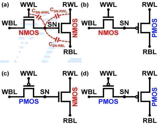
Figure 1.
Schematic diagrams of 2T0C DRAM unit cells with (a) NN, (b) NP, (c) PN, and (d) PP device types.
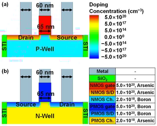
Figure 2.
Cross-sections of 65 nm (a) NMOS and (b) PMOS transistors.

Table 1.
Physical parameter of 65 nm planar transistor.
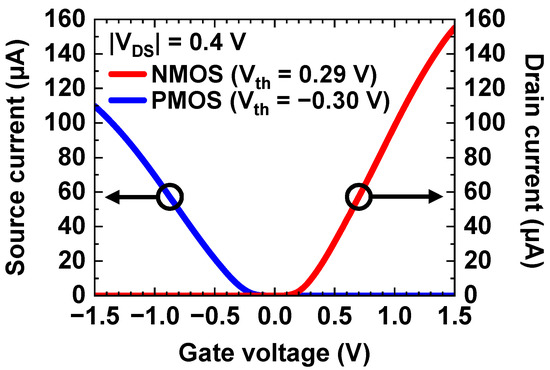
Figure 3.
Transfer characteristics of NMOS and PMOS transistors with Vth of 0.29 V and −0.30 V, respectively.
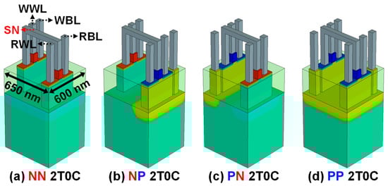
Figure 4.
Three-dimensional structures of 65 nm CMOS-based 2T0C DRAM unit cells with (a) NN, (b) NP, (c) PN, and (d) PP device types.
3. Comparative Analysis of Electrical Characteristics
Figure 5 presents the timing diagrams of the write, precharge, and read operations, and the corresponding VSN curves in the 2T0C DRAM unit cells. After the write operation, a precharge voltage of 0.5 V (½VDD) was applied to the write bitline (WBL), and a long read pulse was applied to RWL and RBL to evaluate the effect of repeated read operations and to measure the retention time. During the write operation, VSN is coupled down in the NN- and NP-type cells and up in the PN- and PP-type cells to VSN_INIT, mainly due to CSN-WWL coupling. During the read operation, VSN is coupled up in the NN- and PN-type cells and down in the NP- and PP-type cells by ΔVSN_READ due to CSN-RWL and CSN-RBL coupling, respectively. The coupling effects during the write and read operations reduce the on/off current ratio, which was measured immediately after a read pulse. Table 2 summarizes VSN_INIT, ΔVSN_READ, and the on/off current ratio in the 65 nm CMOS-based 2T0C DRAM unit cells. Since the coupling direction of VSN for data ‘0’ in the NP- and PN-type cells is the same during the write and read operations, VSN for data ‘0’ in these cells approaches that for data ‘1’ more closely during a read pulse in contrast to the NN- and PP-type cells. As a result, the NP- and PN-type cells exhibit very low on/off current ratios, which can degrade inference accuracy in 2T0C DRAM-based CIM applications.
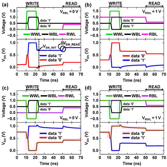
Figure 5.
Timing diagrams of write, precharge, and read operations, and corresponding VSN curves in 2T0C DRAM unit cells with (a) NN, (b) NP, (c) PN, and (d) PP device types.
Table 2.
VSN_INIT, ΔVSN_READ, and on/off current ratio in 65 nm CMOS-based 2T0C DRAM unit cells.
In the 65 nm CMOS-based 2T0C DRAM unit cells, the retention characteristics are mainly affected by the subthreshold leakage current in the write Tr. [9], which is determined by the magnitude of the voltage difference between SN and WBL (VSN-WBL). After the write operation, a large VSN-WBL for data ‘0’ in the NN- and PP-type cells and for data ‘1’ in the NP- and PN-type cells induces a significant subthreshold leakage current, leading to faster deterioration of VSN. Additionally, unlike the NN- and PP-type cells, ΔVSN_READ for data ‘1’ in the NP- and PN-type cells further increases VSN-WBL during a read pulse, thereby accelerating the deterioration of VSN. The retention times for data ‘1’ and data ‘0’ of the 2T0C DRAM unit cells were measured as shown in Figure 6. In this work, the retention time for data ‘1’ was defined as the time required for the initial IREAD for data ‘1’ (IREAD_1) to decrease by 2%. Conversely, the retention time for data ‘0’ was defined as the time required for the initial IREAD for data ‘0’ (IREAD_0) to increase by 2% of the initial IREAD_1. The retention times for data ‘1’ in the NP- and PN-type cells are significantly shorter than those in the NN- and PP-type cells. Considering both the on/off current ratio and the retention time, we conclude that the NP- and PN-type 2T0C DRAM unit cells are not favorable for CIM applications.
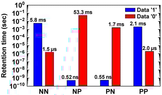
Figure 6.
Retention times for data ‘1’ and data ‘0’ of 65 nm CMOS-based 2T0C DRAM unit cells.
4. Investigation of VSN Fluctuation
As shown in Figure 7, VSN for data ‘0’ (red) in the NN- and PP-type cells fluctuates during the fluctuation interval immediately after a read pulse in contrast to that for data ‘1’ (blue). The reason the fluctuation interval in the PP-type cell is longer than that in the NN-type cell will be discussed at the end of this section. Since the VSN fluctuation can considerably affect the retention time, we identified its cause. Figure 8a and Figure 9a illustrate the equivalent RC models of the NN- and PP-type 2T0C DRAM unit cells after the write operation for data ‘0’, respectively. As shown in Figure 8b and Figure 9b, VSN varies by ΔVSN_READ during the ramp-up and ramp-down of the read pulse. The magnitude of ΔVSN_READ is determined by CSN-RWL and CSN-RBL coupling and further modulated by the coupling effect of the read gate oxide capacitance (COX). VSN in the NN-type cell is coupled up due to CSN-RWL coupling, whereas VSN in the PP-type cell is coupled down due to CSN-RBL coupling, which causes variations in the channel potential of the read Tr. (VREAD_CH) by +ΔV or −ΔV. Simultaneously, VREAD_CH in the NN-type cell increases, while VREAD_CH in the PP-type cell decreases according to the voltage division between RWL and RBL. As a result, VSN is further coupled up or down through COX coupling. As shown in Figure 8c and Figure 9c, the ΔV component in VREAD_CH dissipates through IREAD and VREAD_CH saturates to the divided voltage between RWL and RBL. Subsequently, VSN increases in the NN-type cell and decreases in the PP-type cell due to the subthreshold leakage current in the write Tr., as illustrated in Figure 8d and Figure 9d.
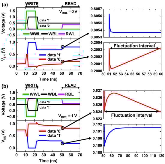
Figure 7.
Timing diagrams and VSN fluctuations for data ‘0’ immediately after a read pulse in (a) NN-type and (b) PP-type cells.
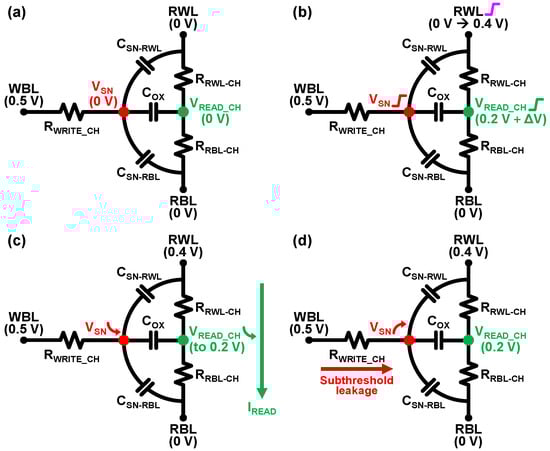
Figure 8.
Equivalent RC models of NN-type 2T0C DRAM unit cell after write operation for data ‘0’ (a) before a read pulse, (b) during a read pulse, (c) immediately after a read pulse, and (d) during retention.
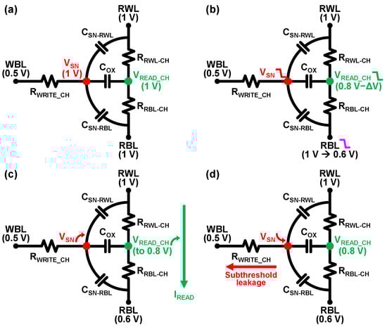
Figure 9.
Equivalent RC models of PP-type 2T0C DRAM unit cell after write operation for data ‘0’ (a) before a read pulse, (b) during a read pulse, (c) immediately after a read pulse, and (d) during retention.
Consequently, the dissipation speed of the ΔV component through IREAD and the subthreshold leakage current can affect the VSN fluctuation interval, and the fluctuation interval may become longer as both IREAD and the subthreshold leakage current decrease. To verify this possibility, we adjusted the body voltage (VB) from 0 V to −1 V in the NN-type cell and from 1 V to 2 V in the PP-type cell, thereby reducing both IREAD and the subthreshold leakage current. Figure 10 shows the VSN fluctuation intervals for data ‘0’ in the NN- and PP-type cells under different VB conditions, where the intervals are extended by 13.8% and 533.4% by VB adjustment, respectively. Since the hole mobility is lower than the electron mobility, both IREAD and the subthreshold leakage current in the PP-type unit cell are lower than those in the NN-type unit cell. Therefore, the fluctuation interval in the PP-type cell is longer than that in the NN-type cell under the initial VB conditions, as shown in Figure 10a,b. Likewise, the fluctuation interval in the PP-type cell becomes significantly wider under the adjusted VB conditions.
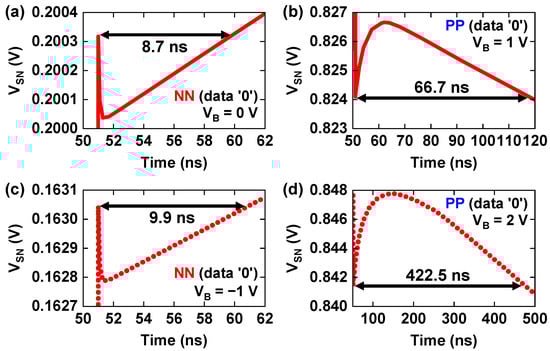
Figure 10.
VSN fluctuation intervals for data ‘0’ in 2T0C DRAM unit cells (a), (c) NN-type at VB = 0 V and −1 V (b), and (d) PP-type at VB = 1 V and 2 V.
5. Conclusions
In this work, we investigated the electrical characteristics of 2T0C DRAM unit cells with the NN, NP, PN, and PP device types for CIM applications. In conclusion, the NN- and PP-type 2T0C DRAM unit cells are relatively suitable for CIM applications, whereas the NP- and PN-type 2T0C DRAM unit cells are not favorable due to their very low on/off current ratios and short retention times. We elucidated the cause of the VSN fluctuation using the equivalent RC models and showed that the fluctuation interval can be extended as both IREAD and the subthreshold leakage current decrease under the adjusted VB conditions. This work is anticipated to make a significant contribution to the analysis of silicon channel-based 2T DRAM.
Author Contributions
Conceptualization, S.K. and W.S.; methodology, S.K. and W.S.; software (Synopsys Sentaurus TCAD V-2023.09), S.K.; validation, S.K.; formal analysis, S.K. and W.S.; investigation, S.K.; resources, S.K. and W.S.; data curation, S.K.; writing—original draft preparation, S.K.; writing—review and editing, S.K. and W.S.; visualization, S.K.; supervision, W.S.; project administration, W.S.; and funding acquisition, W.S. All authors have read and agreed to the published version of the manuscript.
Funding
This research was supported by Seoul National University of Science and Technology.
Data Availability Statement
The data presented in this study are available on request from the corresponding author. The data are not publicly available due to research security.
Acknowledgments
The EDA tool was supported by the IC Design Education Center (IDEC), South Korea.
Conflicts of Interest
The authors declare no conflicts of interest.
References
- Gholami, A.; Yao, Z.; Kim, S.; Hooper, C.; Mahoney, M.W.; Keutzer, K. AI and Memory Wall. IEEE Micro 2024, 44, 33–39. [Google Scholar] [CrossRef]
- Sebastian, A.; Gallo, M.L.; Khaddam-Aljameh, R.; Eleftheriou, E. Memory devices and applications for in-memory computing. Nat. Nanotechnol. 2020, 15, 529–544. [Google Scholar] [CrossRef] [PubMed]
- Cho, S. Volatile and Nonvolatile Memory Devices for Neuromorphic and Processing-in-memory Applications. J. Semicond. Technol. Sci. 2022, 22, 30–46. [Google Scholar] [CrossRef]
- Kwon, D.; Woo, S.Y.; Lee, J.-H. Review of Analog Neuron Devices for Hardware-based Spiking Neural Networks. J. Semicond. Technol. Sci. 2022, 22, 115–131. [Google Scholar] [CrossRef]
- Jang, J.-H.; Shin, J.; Park, J.-T.; Hwang, I.-S.; Kim, H. In-depth Survey of Processing-in-memory Architectures for Deep Neural Networks. J. Semicond. Technol. Sci. 2023, 23, 322–339. [Google Scholar] [CrossRef]
- Shim, W.; Yu, S. Technological Design of 3D NAND-Based Compute-in-Memory Architecture for GB-Scale Deep Neural Network. IEEE Electron Device Lett. 2021, 42, 160–163. [Google Scholar] [CrossRef]
- Whang, S.; Um, S.; Ha, S.; Yoo, H.-J. A Software-Hardware Co-Optimized Sense Amplifier for 2T1C Cell-based DRAM In-Memory-Computing. In Proceedings of the 21st International SoC Design Conference (ISOCC), Sapporo, Japan, 19–22 August 2024. [Google Scholar]
- Xie, S.; Ni, C.; Jain, P.; Hamzaoglu, F.; Kulkarni, J.P. Gain-Cell CIM: Leakage and Bitline Swing Aware 2T1C Gain-Cell eDRAM Compute in Memory Design with Bitline Precharge DACs and Compact Schmitt Trigger ADCs. In Proceedings of the IEEE Symposium on VLSI Technology and Circuits, Honolulu, HI, USA, 12–17 June 2022. [Google Scholar]
- Kong, S.H.; Shim, W. Advanced 2T0C DRAM Technologies for Processing-in-Memory—Part I: Vertical Transistor on Gate (VTG) DRAM Cell Structure. IEEE Trans. Electron Devices 2024, 71, 6633–6638. [Google Scholar] [CrossRef]
- Yook, C.-G.; Shim, W. Advanced 2T0C DRAM Technologies for Processing-in-Memory—Part II: Adaptive Layer-Wise Refresh Technique. IEEE Trans. Electron Devices 2024, 71, 6639–6646. [Google Scholar] [CrossRef]
- Kong, S.; Shim, W. Design of 2T DRAM Cell with Surrounding Poly-Si Capacitor for Enhanced Retention and Mitigated Coupling Effect. IEEE Trans. Device Mater. Rel. 2025, 25, 460–464. [Google Scholar] [CrossRef]
- An, Y.; Kim, H.; Son, D.; Yu, H.; Shim, Y. Dual-Mode 2T1C DRAM Process-In-Memory Architecture for Boolean and MAC Operations. IEEE Access 2025, 13, 133925–133936. [Google Scholar] [CrossRef]
- Zhang, X.; Jo, Y.-J.; Kim, T.T.H. A 65-nm 55.8-TOPS/W Compact 2T eDRAM-Based Compute-in-Memory Macro with Linear Calibration. IEEE Trans. Very Large Scale Integr. (VLSI) Syst. 2025, 33, 1477–1481. [Google Scholar] [CrossRef]
- Yu, C.; Yoo, T.; Kim, H.; Kim, T.T.; Chuan, K.C.T.; Kim, B. A Logic-Compatible eDRAM Compute-In-Memory with Embedded ADCs for Processing Neural Networks. IEEE Trans. Circuits Syst. I Reg. Pap. 2021, 68, 667–679. [Google Scholar] [CrossRef]
- Ha, S.; Kim, S.; Han, D.; Um, S.; Yoo, H.-J. A 36.2 dB High SNR and PVT/Leakage-Robust eDRAM Computing-In-Memory Macro with Segmented BL and Reference Cell Array. IEEE Trans. Circuits Syst. II Expr. Briefs 2022, 69, 2433–2437. [Google Scholar] [CrossRef]
- Tang, W.; Chen, C.; Liu, J.; Zhang, C.; Gu, C.; Duan, X.; Yang, H.; Li, L.; Li, X.; Geng, D. 30 Mb/mm2/layer 3D eDRAM Computing-in-Memory with Embedded BEOL Peripherals and Local Layer-wise Calibration based on First-Demonstrated Vertically-stacked CAA-IGZO 4F2 2T0C Cell. In Proceedings of the International Electron Devices Meeting (IEDM), San Francisco, CA, USA, 9–13 December 2023. [Google Scholar]
- Belmonte, A.; Kundu, S.; Subhechha, S.; Chasin, A.; Rassoul, N.; Dekkers, H.; Puliyalil, H.; Seidel, F.; Carolan, P.; Delhougne, R.; et al. Lowest IOFF < 3×10²¹ A/μm in capacitorless DRAM achieved by Reactive Ion Etch of IGZO-TFT. In Proceedings of the IEEE Symposium on VLSI Technology and Circuits, Kyoto, Japan, 11–16 June 2023. [Google Scholar]
- Gu, C.; Hu, Q.; Zhu, S.; Li, Q.; Zeng, M.; Kang, J.; Tong, A.; Wu, Y. First Experimental Demonstration of 3D-Stacked 2T0C DRAM Cells Based on Indium Tin Oxide Channel. IEEE Electron Device Lett. 2024, 45, 1764–1767. [Google Scholar] [CrossRef]
- Phadke, O.; Kirtania, S.G.; Chakraborty, D.; Datta, S.; Yu, S. Suppressed Capacitive Coupling in 2 Transistor Gain Cell with Oxide Channel and Split Gate. IEEE Trans. Electron Devices 2024, 71, 6749–6755. [Google Scholar] [CrossRef]
- Kwak, J.; Deng, S.; Zhang, C.; Jeong, G.; Phadke, O.; Kirtania, S.G.; Lee, J.; Datta, S.; Yu, S. Machine Learning-Assisted Compact Modeling of AC Stress-Induced Bias Temperature Instability in Top- and Bottom-Gate W-Doped In2O3 Channel Semiconductor Transistors. IEEE Trans. Electron Devices 2025, 72, 4163–4169. [Google Scholar] [CrossRef]
- Chen, C.; Duan, X.; Yang, G.; Lu, C.; Geng, D.; Li, L.; Liu, M. Inter-Layer Dielectric Engineering for Monolithic Stacking 4F2-2T0C DRAM with Channel-All-Around (CAA) IGZO FET to Achieve Good Reliability (>104 s Bias Stress, >1012 Cycles Endurance). In Proceedings of the International Electron Devices Meeting (IEDM), San Francisco, CA, USA, 3–7 December 2022. [Google Scholar]
- Chun, K.C.; Jain, P.; Kim, T.-H.; Kim, C.H. A 667 MHz Logic-Compatible Embedded DRAM Featuring an Asymmetric 2T Gain Cell for High Speed On-Die Caches. IEEE J. Solid-State Circuits 2012, 47, 547–559. [Google Scholar] [CrossRef]
- Chun, K.C.; Zhang, W.; Jain, P.; Kim, C.H. A 700MHz 2T1C embedded DRAM macro in a generic logic process with no boosted supplies. In Proceedings of the IEEE International Solid-State Circuits Conference, San Francisco, CA, USA, 20–23 February 2011. [Google Scholar]
- Choi, W.; Kang, G.; Park, J. A Refresh-Less eDRAM Macro with Embedded Voltage Reference and Selective Read for an Area and Power Efficient Viterbi Decoder. IEEE J. Solid-State Circuits 2015, 50, 2451–2462. [Google Scholar] [CrossRef]
- Somasekhar, D.; Ye, Y.; Aseron, P.; Lu, S.-L.; Khellah, M.M.; Howard, J.; Ruhl, G.; Karnik, T.; Borkar, S.; De, V.K.; et al. 2 GHz 2 Mb 2T Gain Cell Memory Macro with 128 GBytes/sec Bandwidth in a 65 nm Logic Process Technology. IEEE J. Solid-State Circuits 2009, 44, 174–185. [Google Scholar] [CrossRef]
Disclaimer/Publisher’s Note: The statements, opinions and data contained in all publications are solely those of the individual author(s) and contributor(s) and not of MDPI and/or the editor(s). MDPI and/or the editor(s) disclaim responsibility for any injury to people or property resulting from any ideas, methods, instructions or products referred to in the content. |
© 2025 by the authors. Licensee MDPI, Basel, Switzerland. This article is an open access article distributed under the terms and conditions of the Creative Commons Attribution (CC BY) license (https://creativecommons.org/licenses/by/4.0/).