Abstract
The principle of non-Foster broadband matching of electrically small (high-Q) transmitting antennas has been around for more than a few decades. However, there have been only a handful of experimentally proven examples, with highly limited scope of application. The main obstacle is the inherent instability of non-Foster elements, since those are actually active circuits with positive feedback. This research investigates the idea that a common non-Foster transmitter antenna matching network can be replaced with the arrangement of multiple frequency-coherent sources, rendering positive feedback unnecessary. Two different approaches were analyzed, one with a coherent RF current source, the other one with a coherent voltage source. The viability of this idea has been verified by simulations and experimental results. Unlike non-Foster matching, the proposed principle cannot support instability because it does not contain any positive feedback loops. In addition, it offers multiple-octave operational bandwidth, while the efficiency is limited only by the linear operation of the used circuitry, thus remaining at least equal to that of its non-Foster equivalent. While the proof-of-concept experiments were conducted in the lower HF (up to 20 MHz) frequency band, where common antennas are electrically small and highly reactive, there are no physical obstacles to scaling the same principle of operation to higher frequencies.
1. Introduction
Electrically small antenna (ESA) refers to an antenna with physical dimensions much smaller than its operating free-space wavelength [1]. The self-impedance of electrically small antenna is predominantly reactive, while its real part is low. This yields a high Q-factor, which determines the ratio of time-averaged stored energy within the antenna structure to the sum of radiated and dissipated energy. Such impedance characteristics of small antenna results in the low efficiency of power transfer between the antenna and the receiver or transmitter [2]. A classic way to improve power transfer between the antenna and the circuitry is the inclusion of a lumped-element matching network (Figure 1a). However, such a solution comes with a serious drawback imposed by the fundamental Bode–Fano limit; passive (lumped-element) matching is inherently narrowband [3]. One workaround for the Bode–Fano limit is the application of non-Foster elements in matching (Figure 1b) [4]. Non-Foster elements are active electronic circuits that mimic the behavior of hypothetical negative capacitors and negative inductors. The most common approach to non-Foster elements for antenna matching is based on amplifiers with positive feedback that generate required negative input impedance. More specifically, those circuits convert a load impedance into its “negative image” and, therefore, they are usually referred to as negative impedance converters (NICs) [5]. The presence of positive feedback is mandatory in order to generate a phase-shifted response signal (voltage or current). This signal is then superimposed to the original signal in the circuit to cancel out the voltage drop over the reactive part of the antenna impedance. Such a technique results in the antenna impedance, as “seen” by the connected circuitry (receiver or transmitter), appearing to be a real number, consequently improving the efficiency of the small antenna application extensively. This is a well-known principle of non-Foster matching [6,7]. Since the non-Foster elements are built upon the circuits with positive feedback (NICs), they are extremely prone to instability [8,9], i.e., to unwanted oscillations.
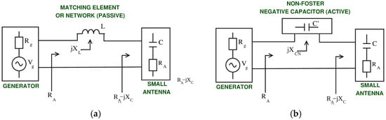
Figure 1.
Small antenna (a) passive matching and (b) non-Foster matching.
The reason why non-Foster matching has been researched and adopted to a greater extent for receivers than for transmitters [10,11] lies in the fact that the stability issues became even more critical and potentially hazardous in the environments with larger power and voltage levels [12].
There are also other methods that attempt to integrate an antenna and transmitter into a broadband, well-matched transmitting system. For example, the approach in [13] uses a conventional “positive-impedance antenna” that is canceled by a non-Foster-based “negative-impedance image”, resulting in a widely tunable (bandwidth up to 10:1), perfectly matched, self-oscillating radiating system. As detailed in [13], this approach can be considered an extension of the classic negative-resistance oscillator. A very recent approach uses switching elements controlled by digital signal processing circuitry [14]. It emulates a source with non-Foster internal impedance and achieves highly efficient matching with a very wide bandwidth (16:1), but only in the very low frequency acoustic regime (100 Hz–1600 Hz). It is important to emphasize that all of these approaches use some form of positive feedback, either analog or digital.
Therefore, we introduce an alternative approach that mimics the operation of non-Foster circuits without any positive feedback and thus completely avoids stability problems. It retains the advantages of non-Foster matching such as broadband operation while circumventing the major problem of non-Foster circuits, which are the stability issues. The evolution of the proposed concept is briefly summarized in Figure 2.
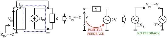
Figure 2.
The evolution from a feedback-based to feedback-less solution for antenna impedance reactive part cancelation: (left) ordinary current inversion NIC; (middle) simplified equivalent circuit; (right) modified equivalent circuit based on two sources (transmitters) without a feedback loop.
A typical non-Foster active matching network based on a current amplifier (Figure 2, left) could be transformed into a voltage-controlled voltage source network (Figure 2, middle). Both networks generate an equal input negative admittance -Y required to cancel out the reactive part of antenna admittance, but, unfortunately, both circuits comprise positive feedback. The proposed concept with two coherent transmitter sources (Figure 2, right) [15] is feedback-less, while at the same time, by manipulation of TX1 and TX2 respective amplitudes and phases, this arrangement effectively emulates the equal negative input admittance -Y at its port, just as the former two circuits.
2. Fundamentals, Materials, and Methods
Although non-Foster matching is applicable both to transmitter and receiver systems, transmitter systems differ in a unique way, which could be used to advantage in order to achieve a non-Foster-like operation without the actual non-Foster circuitry, also circumventing the requirement for positive feedback. Unlike the received signal, which is not known a priori, and it has some arbitrary amplitude and phase, a transmitter generates the signal to be transmitted, hence it bears some predefined amplitude and phase. Therefore, it is generally always feasible to generate another coherent, but phase and amplitude altered signal, to be fed into the antenna, in order to cancel out the reactive part of the antenna impedance. In other words, a second source (transmitter) mimics a purely reactive matching element, but its dispersion characteristic can be tailored almost arbitrarily by its design. Starting with this idea, two different approaches were investigated. Both have in common the traditional concept of an antenna fed by a single transmitter amplifier, commonly supplemented with a matching network and feed line, which is superseded by the 2-source system with the antenna bridged in between them.
2.1. The First Approach: Coherent Current and Voltage Source Antenna–Transmitter System
The generator on the left in Figure 3 is a realistic voltage source with amplitude Vg and internal resistance Rg, while a short dipole antenna is modeled with a series combination of radiation resistance RA and capacitance CA.
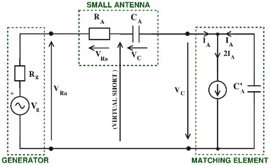
Figure 3.
Controlled current source as transmitter antenna matching element.
The current through antenna and the generator Vg equals IA. Since the impedance of a short antenna is highly reactive, voltage drop VC over CA is high (typically, two or more orders of magnitude higher than voltage drop across RA). In an unmatched circuit operation, connecting only the generator Vg and antenna RA, CA (if the matching element in Figure 3 was shorted out), the radiated power would be extremely low, since only a low fraction of the voltage Vg would be present at RA. If the antenna was passively matched with a series inductor L as a matching element to cancel out the CA voltage drop (as in Figure 1b), the power transfer to RA would have been maximized, but only at the resonant frequency determined by the CA-L series combination, i.e., the operation would have been limited to a very narrow frequency band. Finally, matching using the circuit shown in Figure 3 is capable of both wideband operation and maximal power transfer to RA at the same time. The matching element in Figure 3 comprises a controlled current source and a capacitor C’A which has equal capacitance (CA) as a reactive part of the impedance of a small antenna. To obtain voltage drop across V’C equal to VC across the antenna capacitance CA, but with the opposite sign (to cancel each other out), the current source should provide a current which is equal to the sum of currents through CA and C’A, hence 2IA. It is worth noticing that if voltage drops across CA and C’A cancel each other out, the node “0” between RA and CA becomes virtually connected to ground, and all voltage from the generator output appears across the antenna radiation resistance RA. In other words, the generator “sees” only the real part RA of antenna impedance ZA = RA − jXA. One way to construct such a circuit is to have a current source controlled by the sensing of the current IA through the antenna. In that case, the current source has positive feedback and, loaded with C’A forms a non-Foster element, is prone to instability. Such non-Foster element topology is known as the open-circuit stable (OCS) type [16], and this current source acts as current-controlled current source (CCCS) (i.e., ideal current amplifier). Since this is a transmitter application, there is another way to control the current source without the presence of a feedback loop. Controlling the current source with voltage derived from the generator signal Vg yields a voltage-controlled current source (VCCS), with a transfer function equal to
This results in mesh voltages and currents in the network that are equal to those that would be present in the case of non-Foster matching. In other words, such a circuit mimics the non-Foster matching but without positive feedback. Although the basic idea appears to be quite straightforward and simple, its realization is rather challenging. Current sources are rarely used in RF engineering, especially the ones capable of operation in a wide frequency range. The development of an adequate circuit was indeed a challenging task, and a number of solutions were first considered and tested in simulations. Finally, a circuit based on Howland’s current pump [17] was constructed and tested. Basically, Howland’s current pump can be realized in its simplest form with a single differential amplifier and resistors R1, R2, R3, and R4 as the feedback network around it (Figure 4).
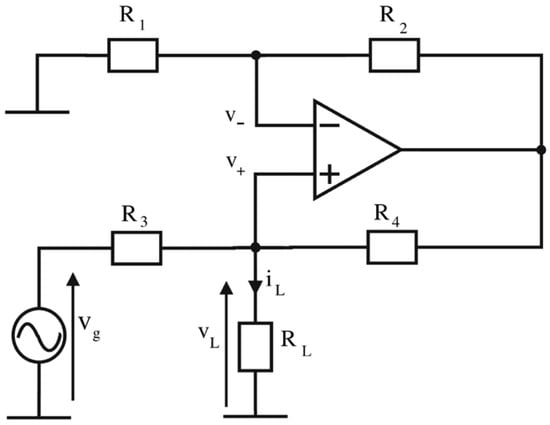
Figure 4.
The basic Howland current source.
When positive and negative feedbacks (Figure 4) are in balance (R2/R1 = R4/R3) the equation for output current becomes very simple, iL = Vg/R3 [17]. Such a basic variant of Howland’s circuit has a serious drawback; it is not possible to obtain both high gain and high input impedance [18]. An additional problem of such a basic arrangement is that the amplifier voltage swing must be substantially higher than the voltage at the load, since R3 and R4 form a voltage divider. As a consequence, the output voltage dynamic range is severely reduced. By splitting R4 (Figure 4) into two resistances (R4 and R5 in Figure 5), with a buffer unity gain amplifier placed between them, the aforementioned drawback can be circumvented. An additional load output buffering to obtain higher output currents, consisting of three OPAMPs, connected in parallel, finally yields the improved circuit, shown in Figure 5.
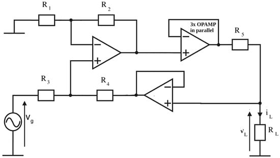
Figure 5.
Circuit diagram of enhanced Howland current source with feedback buffer and output buffer.
This improved Howland’s circuit employs a total of five OPAMPs, two of them voltage-feedback and three (paralleled output buffers) are the current-feedback type.
Howland’s circuit, known from the early years of analog computing, is also referred to in the literature as the Howland integrator or DeBoo integrator [19]; a current source acts as an integrator when loaded with a capacitor, and that is exactly the case with the matching circuit in Figure 3. This poses a problem, since even the slightest input DC imbalance will be integrated, and, consequently, the DC component will steer the output transistors to slip into the saturation region. A solution was found by providing a specially tailored DC path with virtually no measurable influence on RF current source characteristics at operating frequencies.
For a proof of concept, a demonstrator setup was assembled based on the block diagram in Figure 6.
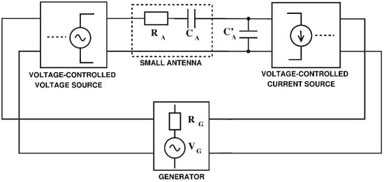
Figure 6.
Block diagram of a demonstrator setup of antenna–transmitter system with coherent current and voltage sources.
Electrical parameters of a small antenna were modeled from the physical dimensions of a dipole operating at 1 MHz (λ = 300 m): length 13 m, wire thickness 1 mm. Using antenna input impedance formulas from [20], the simplest lumped-element model of such an antenna is CA = 100 pF, RA = 1.5 Ω (antenna Q ≈ 1000). The antenna model was physically bridged between two circuit boards: a voltage amplifier (Figure 7, left of the antenna model) and a current source loaded with C’A = CA = 100 pF (Figure 7, right of the antenna model). Both boards were fed with a common RF signal from an RF harmonic generator (which represents the signal to be transmitted in a transmitter system; in a particular application the generator could, of course, be modulated to carry information).
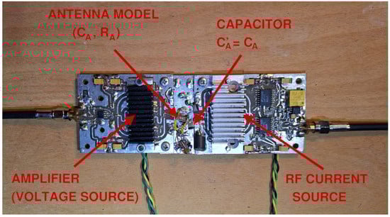
Figure 7.
Prototyped demonstrator of antenna–transmitter system with coherent current and voltage sources.
During the testing phase it was determined that the operation is feasible up to frequency of 8 MHz. This upper bound was imposed by the operational bandwidth of the used current source. Simulation and measurement results of this demonstrator system are given in Section 3.
2.2. The Second Approach: Coherent Multiple Voltage Source Antenna–Transmitter System
Although the viability of a previously described solution based on VCCS that closely mimics the operation of a “true” non-Foster matching element was experimentally confirmed with results in a frequency range up to 8 MHz, it has several drawbacks. The RF current source is rather complicated in construction and it contains multiple feedback loops, which limit its speed of operation. The plausibility of scaling up to another, higher frequency range is questionable. Another, more straightforward solution was pursued.
The model shown in Figure 8a could be described as the traditional non-Foster approach to broadband matching with OCS negative capacitance (the very same model was the starting point in the first approach elaborated in Section 2.1). The same principle is applicable to the receiver system, where a receiver input would be positioned instead of a generator VG, and energy flow would be reversed from the antenna to the receiver input. Both in transmitter and receiver systems, an IA-controlled current source provides the doubled current 2IA; the feedback between the 2IA source and IA is clearly positive.
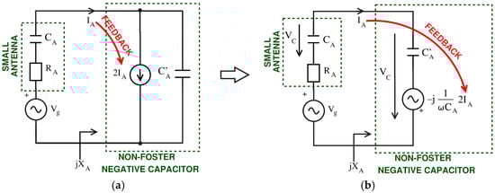
Figure 8.
(a) Matching with OCS non-Foster element; (b) Norton-transformed equivalent of the circuit from Figure 8a.
Since current sources in the RF frequency range are inconvenient and hard to practically realize, there is a workaround to avoid the current source by transformation of the 2IA-CA’ shunt network to an equivalent Thevenin voltage generator Vg’ with series CA’ (Figure 8b) [21]. Thevenin transformation is still applicable for both transmitting and receiving systems, and the operation of non-Foster circuits based on voltage-mode devices has been experimentally verified [22]. The network in Figure 8b can be realized with a current-controlled voltage source (CCVS) (i.e., a trans-impedance amplifier), using a sensing signal of antenna current IA as the input. It is still a non-Foster network with positive feedback, and further development towards the feedback-less system is possible exclusively for transmitting systems. Instead of quite uncommon CCVS, it is much simpler to make use of a voltage-controlled voltage source (VCVS), which is just another name for a voltage amplifier. The supplementary generator Vg’ should provide voltage equal to
Since Vg’ is no more controlled by sensing of current IA, but rather it is a linear function of “main” generator voltage Vg, the system becomes feedback-less. From (2) it is clear that voltage is shifted by -90 degrees and amplitude is inversely proportional to frequency ω. Another important fact worth noticing is that in Figure 8b capacitances CA’ and CA are now connected in series, and since those two are of equal value, the voltage drops across CA and CA’ are equal (Figure 9a).
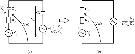
Figure 9.
(a) Feedback-less equivalent of the circuit from Figure 8b, derived through conversion from CCVS to VCVS; (b) Further simplification of the circuit by omission of CA’.
One could look at the series pair CA-CA’ as a single capacitor with total capacitance of CA/2. This in turn means that CA’ becomes redundant (Figure 9b) if the Vg’ voltage is to be lowered by half, therefore the supplementary source V’g should provide voltage V’g equal to (3)
An additional advantage of reduction in V’g by half is that it practically doubles the dynamic range of the system with no change in supply rail voltages. Further convenience is that such a coherent signal (3) could be derived from main source Vg with basic electronic circuitry in a surprisingly straightforward manner: both −90 degrees phase shift and 1/ω amplitude roll-off could be achieved with a simple and well-known network: a low-pass filter operating far below its cut-off frequency.
Unlike the circuits in Figure 8, the system depicted in Figure 10 is evidently feedback-less and stability is no longer an issue. But, the advantage over “true” non-Foster goes further beyond this. The properties of realistic non-Foster circuits differ to a great extent from their ideal models [23]. Moreover, the realistic ones have to be kept safely from the edge of stability [24]. Consequently, this degrades practical performance in canceling antenna reactance compared to what would be achieved with an ideal, so far only theoretically achievable, non-Foster circuit. Time-domain simulations of an antenna–transmitter system in Figure 10 have confirmed that the voltage signals are correctly phased and exhibit correct amplitudes as they would have been with a “true” non-Foster circuit instead of Vg’ (Figure 11a, top and middle plot). As expected, voltage at the node between RA and CA is negligible (Figure 11a, lower plot), i.e., the node acts like a virtual short to ground.
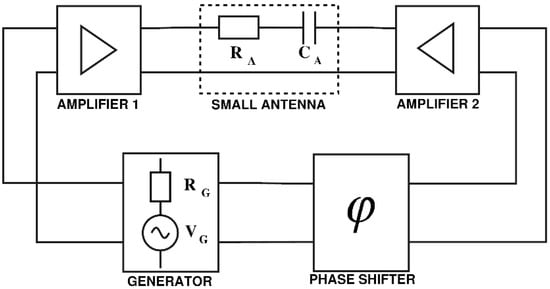
Figure 10.
Block diagram of 2-source high-Q antenna transmitter model.
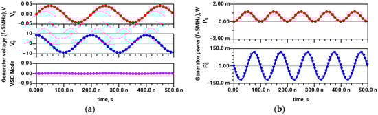
Figure 11.
Time-domain simulated (a) voltages of generator Vg (in-phase), generator Vg’ (quadrature), and voltage at the node between RA and CA (virtual short circuit to ground, “VSC Node”); (b) instantaneous power flow from respective generators Pg and Pg’.
Physically, this occurs because the Vg’ source generates a flow of inductive reactive power that is exactly opposite to the capacitive reactive power flow through the capacitance CA. This can be seen from the plots in Figure 11b, which show the instantaneous power flow from the generators Vg and Vg’. It is worth noticing that the power flow from the main (in-phase) generator Vg is always positive. The generator supplies the real (active) power to the load RA, while the power flow associated with the Vg’ (quadrature) generator has positive and negative values (and also much larger power swing), but its mean value is zero. The explanation is that power swings back and forth between the antenna capacitance CA and the generator Vg’. Thus, this power flow represents pure reactive power. This is exactly equal to the behavior of the antenna circuit matched using ordinary series LC resonance. Of course, the advantage is that this active “reactive cancelation” in the proposed method is the absence of any transient state, which means infinite cancelation bandwidth. Thus, the additional source indeed behaves as ‘negative’ non-Foster capacitance causing broadband matching, but without existence of any positive feedback loop. In practice, however, inevitable imperfections will limit the bandwidth. Therefore, the achieved bandwidth will be finite but still extremely broadband. The crucial difference in the behavior between the passive and active matching circuits can be observed by analysis of the transient state (thus, the analysis in the short period following the system power-up), as shown in Figure 12 and Figure 13.
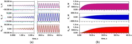
Figure 12.
Transient simulation of passive matching system of short dipole (RA = 1.5 Ω, CA = 100 pF) based on series inductance (L = 10.13 µH), with the signal frequency of 5 MHz. (a) Generator current (Ig), the voltage at matching element (inductor) (VL), and the voltage at the real part of antenna impedance (VRa); (b) Instantaneous power flow from generator (Pg), power flow through passive matching element (inductor) (PL), and antenna radiated power (PRa).
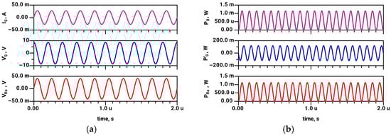
Figure 13.
Transient simulation of active (dual-source) matching system of short dipole (RA = 1.5 Ω, CA = 100 pF), with the signal frequency of 5 MHz. (a) Main (in-phase) generator current (Ig), the voltage at second transmitter (Vg’), and the voltage at a real part of antenna impedance (VRa); (b) Instantaneous power flow from generator (Pg), power flow through second transmitter (second generator) (Pg’), and antenna radiated power (PRa).
The passive matching system (Figure 12) takes approximately 40 µs (200 periods) to reach the steady-state operation, unlike active dual-source system (Figure 13), where no transient phenomenon can be observed; the radiated power of the active dual-source system is constant immediately upon power-up. The significant difference in matching bandwidth between a passive and an active dual-source system could be observed through comparison of Figure 14 and Figure 15, particularly regarding the radiated power. The operating frequency is here altered merely by 10% (from 5 MHz to 4.5 MHz).
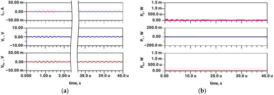
Figure 14.
Transient simulation of passive matching system of short dipole (RA = 1.5 Ω, CA = 100 pF) based on series inductance (L = 10.13 µH), frequency of 4.5 MHz (0.9f0, f0 being the central (resonant) frequency): (a) Generator current (Ig), the voltage at second transmitter (Vg’), and the voltage at a real part of antenna impedance (VRa); (b) Instantaneous power flow from generator (Pg), power flow through second transmitter (second generator) (Pg’), and antenna radiated power (PRa).
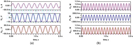
Figure 15.
Transient simulation of active (dual-source) matching system of short dipole (RA = 1.5 Ω, CA = 100 pF), with the signal frequency of 4.5 MHz (0.9f0, f0 being the central frequency): (a) Main (in-phase) generator current (Ig), the voltage at second transmitter (Vg’), and the voltage at a real part of antenna impedance (VRa); (b) Instantaneous power flow from generator (Pg), power flow through second transmitter (second generator) (Pg’), and antenna radiated power (PRa).
The results in Figure 14 (passive case) reveal that the steady-state voltage VL at the matching element (inductor) is substantially lower than in Figure 12. This is expected, as the frequency 4.5 MHz differs from the matching (resonant) frequency of 5 MHz, and passive matching is inherently narrowband [2]. Consequently, the antenna radiated power at 4.5 MHz in Figure 14 is several orders of magnitude lower compared to the radiated power PRa in Figure 12. On the other hand, all of the observed voltage and power levels in the active (dual-source) system are nearly equal at 5 MHz (Figure 13) and at 4.5 MHz (Figure 15). Thus, one could confirm that antenna matching is broadband in the case of an active two-generator system.
The proposed dual-source concept was verified on an experimental demonstrator setup (Figure 16 and Figure 17). In order to provide a sufficient voltage swing at the antenna, which is, for a high-Q antenna, considerably high, RF amplifiers with higher voltage supply rails should be utilized at both sides of the antenna bridge. Hence, dedicated amplifier blocks were constructed for this purpose. It has also been taken into consideration that a low-pass filter operating far below its cutoff frequency inevitably imposes significant attenuation in a signal path, therefore a cascaded three amplifier gain stage block had to be included in a low-pass filter path. Total voltage gain of this block is A = 250, and it is realized with three HFA1130 current-feedback RF OPAMPs [25]. Time-domain simulations with actual amplifier models revealed that the phase delay of those three stages combined is not negligible. In order to compensate for the phase delay, a three-stage unity-gain amplifier block was included in the path of main generator Vg (Figure 16 and Figure 17) as a phase delay compensation. The cutoff frequency of the low-pass filter (that provides -90° phase shift) is 100 times larger than the operation frequency of the system, which in turn results in a negligible phase error of merely 0.6°.
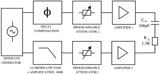
Figure 16.
Block diagram of coherent multiple voltage source antenna–transmitter demonstrator system.
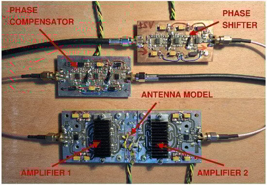
Figure 17.
Experimental RF demonstrator setup of a multiple voltage source antenna–transmitter.
In order to accurately resemble the operation of an ideal non-Foster matching network, the constructed 2-source bridge should be “balanced” in the manner that the Vg generator signal magnitude equals the voltage drop over RA, while Vg’ signal magnitude equals voltage drop over CA’. With these requirements met, the node between RA and CA becomes virtually short circuited to the ground. Therefore, in an ideally balanced system, the generator Vg virtually drives purely real load RA, while Vg’ virtually drives solely antenna reactance CA. Bearing in mind that for antenna with large Q the voltage drop over reactive part CA is two or more orders of magnitude higher than the voltage drop over radiation resistance RA, and programmable attenuators in both signal paths were introduced to balance the bridge amplitudes precisely. Once the system balanced, it remains such, regardless of signal frequency. In other words, the wideband operation is assured.
For the practical realization of the demonstrator system, dedicated circuitry had to be developed and crafted (Figure 17). Since the load impedance is not even close to 50 Ohm as in traditional transmitters, antenna feed lines should not be used, but instead the amplifier bridge output and antenna model input are connected as close as physically possible (Figure 17). The signal was generated using a DDS harmonic generator, while the amplifiers 1 and 2 (Figure 17) were identical. In the schematic diagram in Figure 9b the generator Vg’ has a positive output connected to the negative output of Vg. For practical realization with single-ended amplifiers this is inconvenient, hence two counterphase outputs from the sinewave generator were used and both amplifiers had output referenced to the ground. Instead of a counterphase generator output, an inverting unity gain stage could have been used in the signal path of either amplifier 1 or amplifier 2.
Each amplifier is a cascaded two-stage unit, where each stage has a gain of A = 10 realized with THS3091 off-the-shelf class-AB RF OPAMPs [26]. The second stage has three OPAMPs connected in parallel for extensive output current handling and lower output resistance. With power supply rails of 32 V (which is also the maximum rated by the manufacturer), the unsaturated output voltage swing is up to 26 Vp-p. The radiated power of the entire system as well as the lower frequency limit are both determined by the voltage swing of the lower amplifier in Figure 16 (since it provides Vg’ phase-offset signal to cancel out the vast voltage drop over CA).
3. Measurement Results
Measurement results for both approaches were obtained with power supply ±16 V and an RC model of a small antenna (RA = 1.5 Ω, CA = 100 pF, Q = 1000 at 1 MHz).
3.1. Measurement Results of Coherent Current and Voltage Source System
Results in Figure 18 have shown that the power level dissipated on antenna resistance model RA was constant across three octaves (from 1 to 8 MHz). Time-domain circuit simulation results in the Advanced Design System (ADS) circuit simulator [27] are given in the same Figure 18, obtained with SPICE models of all active elements used in the demonstrator.
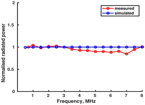
Figure 18.
Radiated power of coherent current and voltage source system (power level relative to simulated result at the lowest operating frequency).
For achieving such a wide frequency range, an extremely high output voltage dynamic was required, since Q spans from 1000 to 130. Observable deviation between the simulation and experimental results were attributed to circuit board parasitics and slightly dispersive current source transfer characteristics. The measured equivalent radiated power was low (less than a milliwatt), but it is noteworthy that equally low, or even lower, power would be measured in case of a “true” non-Foster circuit using the equal supply rail voltages and antenna model. For both circuits the same constraint applies, which is the highest allowed voltage swing at the output of active devices.
Obtaining an accurate power measurement of the antenna radiation resistance hardware model (resistor RA) was a challenging task. The main problem was that neither terminal of RA is grounded (Figure 16), as RA is connected between the two amplifier outputs, making RA a “floating” load. To measure a low differential voltage across RA while the common-mode voltage is several orders of magnitude higher, an RF transformer (balun) CX2040LNL [28] was used (Figure 19) to feed the standard ground-referenced (asymmetrical) high-impedance oscilloscope input.
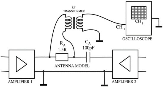
Figure 19.
Differential radiating signal measurement setup.
The transformer is rated to have a flat response from 0.5 MHz to 100 MHz within 0.3 dB. Because the transformer introduces an additional voltage transfer error, correction was required. The transfer characteristics of the particular transformer were recorded and then applied to correct the measured differential radiating signal. Since the voltage at RA is in the millivolt range, to suppress noise and interference, the oscilloscope’s measurement averaging function (128-point average) was used. The estimated total measurement error for the setup in Figure 19 was within ±5%.
3.2. Measurement Results of Coherent Multiple Voltage Sources System
The results of radiated power measurement are shown in Figure 20. The normalized radiated power exhibits flatness (within ±10%) over more than three octaves. For comparison, time-domain simulation results are given in the same Figure 20, obtained with SPICE models of all active elements (OP-amps). Discrepancy between the measured and simulated results could be attributed to circuit layout parasitics (above all, the PCB trace lengths), and slight output level compression at high voltage swings, which occurs at the bottom of the operating frequency band.
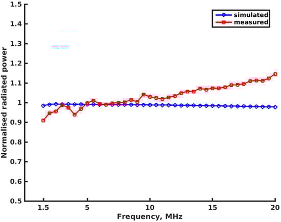
Figure 20.
Radiated power of coherent multiple voltage sources system (power level relative to simulated result at the lowest operating frequency).
The measured power level was around 0.13 mW (−10 dBm). Although this is indeed a low power level, it is important to stress that at best an equal power would be achieved with equivalent “true” non-Foster matching with an active non-Foster element under equal conditions. Achieving higher radiated power remains a fundamental problem of small antennas, regardless of matching technique (even in the case of passive matching). In any case, the radiated power is constrained by maximal amplitude of the voltage signal across the compensating element.
Since the problem of millivolt-scale voltage measurement on the floating antenna hardware model exists as in the voltage source approach, the same measurement technique using a transformer and oscilloscope was applied, as previously described in Section 3.2 (Figure 19). Thus, measurement error estimates are also equal, within ±5%.
3.3. Comparison of the Coherent Current Source and Coherent Voltage Source Experiment Results
The comparison of the most important features of the two proposed approaches is summarized in Table 1.

Table 1.
Performance comparison of current source and voltage source approach.
In-detail elaboration about the differences in results from Table 1 and the related causes follows.
3.3.1. Maximum Operating Frequency
For the coherent current source system, the maximum operating frequency was 8 MHz, which is 2.5 times lower than the 20 MHz achieved by the coherent voltage source system. The output buffers of both the current source and voltage source blocks used the same extremely fast operational amplifiers. However, the current source consists of multiple interconnected amplifiers with global feedback; such topology significantly reduces the maximum operating frequency.
3.3.2. Output Voltage Swing (and Consequently, Maximum Output Power)
Since current source with shunt capacitor CA’ (Figure 3) resembles the “true” non-Foster element more consistently, that in turn means it also introduces an additional large voltage drop in the circuit. This voltage drop is superimposed to the counterphase voltage drop across the antenna CA and cancels out the antenna reactance. Let us suppose that the current source has an equal output voltage swing as quadrature voltage source output (amplifier 2 in Figure 16) in coherent voltage source system. Under those equal conditions, the dynamic range of voltage available for cancelation of the antenna reactance is reduced to half in the current source system (since CA and CA’ are connected in the series), hence the maximum antenna radiated power is reduced to 1/4 for the current-source-based solution.
3.3.3. Complexity
The coherent current source system demonstrator utilizes nine OPAMPs in total, while the coherent voltage system demonstrator has a total of fourteen OPAMPs. Despite this, the coherent voltage system is still more straightforward since all the stages are simple circuits with local (negative) feedback. Although all of the stages in both systems introduce inevitable delay (which results in phase errors), the coherent voltage source system is built almost symmetrically around the antenna, which means that the phase errors in both signal paths are mutually compensated to the greatest extent in this system.
4. Discussion
It is worth touching upon energy efficiency considerations related to conducted experiments. Linear amplifiers like the ones used in the demonstrators (AB-class) are extremely inefficient in the regime of small output signal (in regard to supply voltage) [29]. In both proposed systems, the main “in-phase” source provides only a small voltage to be dissipated at RA, while the other source has to provide an extremely high output voltage swing. At the same time, the power supply voltage for both sources has to be equal. Hence, the main “in-phase” amplifier is always in a low excitation regime and utterly inefficient. One way to somewhat improve efficiency would be to introduce voltage supply tracking locked to the signal amplitude, a technique that has been investigated and found feasible according to [30]. Another downside of linear (class-AB) amplifiers is low efficiency when driving highly reactive loads [31]. As shown in Figure 11b, the instantaneous power vs. time diagram shows that power swings back and forth between generator Vg’ and antenna reactance CA. How the circuitry handles this power greatly affects the efficiency of the system. If the power reflected from the load is dissipated in the generator in each cycle, which generally happens if linear amplifiers are used as generator output, the efficiency will be extremely low. However, some subsequent research on the matter has revealed [32] that non-linear (switch-mode) output stages along with appropriate filtering and power supply could “recycle” a fair amount of reflected energy. This could consequently enable significant improvements in efficiency. The utilization of circuits in a non-linear (time-discrete, switched) mode of operation was not considered in this research due to the complexity of the matter; however, the authors find it as one of the preferred directions for further research.
The fact that linear (class-AB) amplifiers exhibit low efficiency when driving highly reactive loads bolsters the conclusion that “true” non-Foster elements are unlikely to improve overall efficiency in transmitting systems, since non-Foster elements are in fact positive-feedback amplifiers loaded with pure reactance, hence the highly inefficient circuits in the first place. Although this research shows that there are techniques to tackle the problem of high reactance of a high-Q load, even with the reactive part canceled out, another major problem persists, and that is how to efficiently drive the extremely low radiation resistance of small antenna.
The consistency of the used simplified antenna model (constant-value CA, RA) may be questioned since the precise model should take into account the dispersion of radiation resistance RA. One way of performing that would be the use of the Chu’s formula [20]. It is important to notice that the original Chu’s article [33] does not present an equation for the antenna self-impedance, instead it predicts the impedance of particular spherical waves. However, the equivalent ladder networks of these two impedances are of the same form, which justifies the use of the first approximation of the input impedance by Chu’s Equation (4):
In expression (4) a is the length of dipole, c is speed of light, so it is evident that the RA increase is proportional to the square of the operating frequency. This also greatly affects antenna Q. It is true that taking into account RA dispersion would be beneficial. In order to further improve output power level flatness in the broad frequency range, the amplitude of the main generator Vg should be scaled up in proportion to the frequency. Such a modification in both proposed approaches is feasible without complicated circuitry. However, since this research’s major objective was to investigate the phenomenon of cancelation of antenna reactance (particularly the comparison of “real” non-Foster and feedback-less non-Foster-like solutions), tackling this with RA dispersion was not an essential issue this time, and it was omitted for simplicity.
Finally, Table 2 provides a concise comparison of the main advantages and disadvantages of classical passive matching, active non-Foster matching, and the active dual-source approach presented in this work. It clearly shows that the dual-source approach offers at least as broad a matching bandwidth as the classical non-Foster approach, but without stability problems. For a fair comparison, it should be noted that the dual-source approach, just like the non-Foster approach, cannot solve the occurrence of high-voltage signals, which are related to basic physics (broadband resonant-like cancelation).
Table 2.
A concise comparison of passive matching, active non-Foster matching, and dual-source-based active matching.
5. Conclusions
Results have shown that both proposed approaches mimic the operation of a non-Foster element in antenna matching, while circumventing the major problem of “true” non-Foster elements: the positive feedback and related instability issues. The advantage of the feedback-less approach goes a bit further; while “real” non-Foster circuits have to be kept safely in a stable operating region, which in turn means that antenna reactance cancelation effect is never achieved in full, the proposed substituted solution operates just as a nearly idealistic non-Foster circuit at the edge of stability and thus provides a full cancelation of antenna reactance.
The main objective of this research was to re-evaluate non-Foster and similar techniques for matching highly reactive RF loads, confirming that other viable solutions exist without the downsides of non-Foster circuits, which could yield comparable or even better results. Upscaling to higher power levels and shifting to a non-linear operating regime using switching circuits were not within the scope of this research, but the authors consider these topics highly important for future work.
Author Contributions
Conceptualization, A.K. and S.H.; methodology, A.K. and S.H.; software, A.K.; validation, A.K. and S.H.; formal analysis, A.K. and S.H.; investigation, A.K. and S.H.; resources, A.K. and S.H.; data curation, A.K.; writing—original draft preparation, A.K. and S.H.; writing—review and editing, A.K. and S.H.; visualization, A.K.; supervision, S.H.; project administration, S.H. All authors have read and agreed to the published version of the manuscript.
Funding
This work was supported in part by the projects “General Stability Theory of non-Foster and Time-varying Elements” (EOARD grant FA8655-22-1-7055) and “Active and Reconfigurable Electromagnetic Structures and Systems” (HRZZ grant IP 2022-10-2351).
Data Availability Statement
The raw data supporting the conclusions of this article will be made available by the authors on request.
Conflicts of Interest
The authors declare no conflicts of interest.
Abbreviations
The following abbreviations are used in this manuscript:
| ESA | Electrically small antenna |
| OCS | Open-circuit stable |
| OPAMP | Operational amplifier |
| CCCS | Current-controlled current source |
| VCCS | Voltage-controlled current source |
| CCVS | Current-controlled voltage source |
| VCVS | Voltage-controlled voltage source |
| DC | Direct current |
| SPICE | Simulation Program with Integrated Circuit Emphasis |
References
- Hansen, R.C. Electrically Small, Superdirective, and Superconducting Antennas; Wiley: Hoboken, NJ, USA, 2006. [Google Scholar]
- Wheeler, H.A. Fundamental limitations of small antennas. Proc. IRE 1947, 35, 1479–1484. [Google Scholar] [CrossRef]
- Fano, R.M. Theoretical Limitations on the Broadband Matching of Arbitrary Impedances; Technical Report No. 41; Research Laboratory of Electronics, Massachusetts Institute of Technology: Cambridge, MA, USA, 1948. [Google Scholar]
- Sussman-Fort, S.E. Non-Foster Impedance Matching of Electrically-Small Antennas. IEEE Trans. Antennas Propag. 2009, 57, 2230–2241. [Google Scholar] [CrossRef]
- Linvill, J.G. Transistor Negative Impedance Converters. Proc. IRE 1953, 41, 725–729. [Google Scholar] [CrossRef]
- Sussman-Fort, S.E. Matching Network Design Using Non-Foster Impedances. Int. J. RF Microw. Comput.-Aided Eng. 2006, 16, 135–142. [Google Scholar] [CrossRef]
- Buyantuev, B.; Kholodnyak, D. Applications of non-Foster elements to design advanced RF and microwave devices. In Proceedings of the 2018 IEEE Conference of Russian Young Researchers in Electrical and Electronic Engineering (EIConRus), Moscow and St. Petersburg, Russia, 29 January–1 February 2018; pp. 1656–1660. [Google Scholar] [CrossRef]
- Stearns, S.D. Circuit stability theory for non-Foster circuits. In Proceedings of the 2013 IEEE MTT-S International Microwave Symposium Digest (MTT), Seattle, WA, USA, 2–7 June 2013; pp. 1–3. [Google Scholar] [CrossRef]
- Ugarte-Muñoz, E.; Hrabar, S.; Segovia-Vargas, D.; Kiricenko, A. Stability of Non-Foster Reactive Elements for use in Active Metamaterials and Antennas. IEEE Trans. Antennas Propag. 2012, 60, 3490–3494. [Google Scholar] [CrossRef]
- Shih, T.Y.; Behdad, N. Wideband, Non-Foster Impedance Matching of Electrically Small Transmitting Antennas. IEEE Trans. Antennas Propag. 2018, 66, 5687–5697. [Google Scholar] [CrossRef]
- Sussman-Fort, S.E.; Rudish, R.M. Non-Foster Impedance Matching for Transmit Applications. In Proceedings of the IEEE International Workshop on Antenna Technology Small Antennas and Novel Metamaterials, White Plains, NY, USA, 6–8 March 2006; pp. 53–56. [Google Scholar] [CrossRef]
- Rowe, T.; Shih, T.Y.; Behdad, N. Power-Handling Capabilities of Non-Foster Impedance-Matching Networks: Using gridded vacuum tubes and power transistors. IEEE Trans. Antennas Propag. 2018, 60, 60–69. [Google Scholar] [CrossRef]
- Vincelj, L.; Krois, I.; Hrabar, S. Toward self-oscillating non-Foster unit cell for future active metasurfaces. IEEE Trans. Antennas Propag. 2020, 68, 1665–1679. [Google Scholar] [CrossRef]
- Yang, X.; Zhang, Z.; Xu, M.; Li, S.; Zhang, Y.; Zhu, X.-F.; Ouyang, X.; Alù, A. Digital non-Foster-inspired electronics for broadband impedance matching. Nat. Commun. 2024, 15, 4346. [Google Scholar] [CrossRef] [PubMed]
- Kiricenko, A.; Hrabar, S. Non-Foster-inspired Two-transmitter System based on Coherent Current/voltage Sources. In Proceedings of the 2022 IEEE International Symposium on AP and USNC-URSI Radio Science Meeting (AP-S/URSI), Denver, CO, USA, 10–15 July 2022; pp. 1308–1309. [Google Scholar] [CrossRef]
- Brownlie, J. On the stability properties of a negative impedance converter. IEEE Tran. Circuit Theory 1966, 13, 98–99. [Google Scholar] [CrossRef]
- Texas Instruments. AN-1515: A Comprehensive Study of the Howland Current Pump; Application Report SNOA474A; Texas Instruments: Dallas, TX, USA, 2008. [Google Scholar]
- Yiang, N. A Large Current Source with High Accuracy and Fast Settling; Analog Dialogue; Analog Devices: Wilmington, MA, USA, 2018; Volume 52-10, Available online: https://www.analog.com/en/resources/analog-dialogue/articles/a-large-current-source-with-high-accuracy-and-fast-settling.html (accessed on 14 October 2025).
- DeBoo, G.J. Feedback Integrator with Grounded Capacitor. U.S. Patent US3470495A, 30 September 1969. [Google Scholar]
- Fujimoto, K.; Morishita, H. Modern Small Antennas; Cambridge University Press: Cambridge, UK, 2013. [Google Scholar] [CrossRef]
- Kiricenko, A.; Hrabar, S. Quadrature non-Foster-inspired Matching of Short Transmitting Dipole: Basic Preliminary Experiments. In Proceedings of the 2019 23rd International Conference on Applied Electromagnetics and Communications (ICECOM), Dubrovnik, Croatia, 30 September–2 October 2019; pp. 1–3. [Google Scholar] [CrossRef]
- Hrabar, S.; Krois, I.; Bonić, I.; Kiricenko, A. Negative capacitor paves the way to ultra-broadband metamaterials. Appl. Phys. Lett. 2011, 99, 254103. [Google Scholar] [CrossRef]
- Hrabar, S.; Okorn, B.; Ciganović, V.; Krois, I. Ideal versus realistic non-Foster elements in active metamaterials. In Proceedings of the 2014 IEEE Antennas and Propagation Society International Symposium (APSURSI), Memphis, TN, USA, 6–11 July 2014; pp. 1240–1241. [Google Scholar] [CrossRef]
- Stearns, S.D. Stable band-pass non-Foster circuits. In Proceedings of the 2015 IEEE International Symposium on Antennas and Propagation & USNC/URSI National Radio Science Meeting, Vancouver, BC, Canada, 19–24 July 2015; pp. 1386–1387. [Google Scholar] [CrossRef]
- Renesas Electronics. HFA1130 Datasheet. Available online: https://www.renesas.com/en/document/dst/hfa1130-datasheet (accessed on 14 October 2025).
- Texas Instruments. THS3091 Datasheet. Available online: https://www.ti.com/lit/ds/symlink/ths3091.pdf (accessed on 14 October 2025).
- Keysight. Advanced Design System (ADS). Available online: https://www.keysight.com/us/en/products/software/pathwave-design-software/pathwave-advanced-design-system.html (accessed on 14 October 2025).
- Pulse Electronics. CX2040LNL Datasheet. Available online: https://productfinder.pulseeng.com/doc_type/WEB301/doc_num/CX2040LNL-01/doc_part/CX2040LNL.pdf (accessed on 22 November 2025).
- Cripps, S. Advanced Techniques in RF Power Amplifier Design; Artech: Morristown, NJ, USA, 2002. [Google Scholar]
- Rasty Boroojeni, S.; Sadrpour, M.; Adib, E. Class AB amplifier with simultaneous amplitude and output current tracking. In Proceedings of the 20th Iranian Conference on Electrical Engineering (ICEE2012), Tehran, Iran, 15–17 May 2012; pp. 358–363. [Google Scholar] [CrossRef]
- Hajek, K. Efficiency of the Class B-CE and Class B-CC High Voltage Wideband Amplifiers with a Capacitive Load. In Proceedings of the 21st International Conference (Radioelektronika 2011), Brno, Czech Republic, 19–20 April 2011. [Google Scholar]
- Kiricenko, A. Non-Foster Radio Frequency Source. Ph.D Thesis, University of Zagreb, Zagreb, Croatia, 2019. [Google Scholar]
- Chu, L.J. Physical Limitations of OmniDirectional Antennas; Technical Report No. 64; Research Laboratory of Electronics, Massachusetts Institute of Technology: Cambridge, MA, USA, 1948. [Google Scholar]
Disclaimer/Publisher’s Note: The statements, opinions and data contained in all publications are solely those of the individual author(s) and contributor(s) and not of MDPI and/or the editor(s). MDPI and/or the editor(s) disclaim responsibility for any injury to people or property resulting from any ideas, methods, instructions or products referred to in the content. |
© 2025 by the authors. Licensee MDPI, Basel, Switzerland. This article is an open access article distributed under the terms and conditions of the Creative Commons Attribution (CC BY) license (https://creativecommons.org/licenses/by/4.0/).