Article

A 0.3 V High-Efficiency Bulk-Driven Rail-to-Rail OTA with High Gain-Bandwidth for Wearable Applications

School of Geophysics and Information Technology, China University of Geosciences, Beijing 100083, China
*
Author to whom correspondence should be addressed.
Electronics 2025, 14(23), 4702; https://doi.org/10.3390/electronics14234702
Submission received: 30 October 2025 / Revised: 25 November 2025 / Accepted: 25 November 2025 / Published: 28 November 2025

Abstract

This paper presents a high-efficiency, nW-level operational transconductance amplifier (OTA) capable of operating at 0.3 V with rail-to-rail input and output. The design utilizes a bulk-driven technique in the input stage to extend the common-mode input range under ultra-low-voltage conditions. A simplified intermediate stage ensures reliable MOS operation at ultra-low-voltage levels while reducing power consumption, and a modified Class-AB controlled output stage facilitates rail-to-rail output and enhances current efficiency. Fabricated using SMIC 0.18 μ m technology and operating at a 0.3 V supply, the OTA achieves a DC gain of 63.07 dB, phase margin of 61.5°, a gain-bandwidth product of 37.68 kHz, and a slew rate of 21.85 V/ms while consuming only 123 nW with a 60 pF load. The design also demonstrates superior small-signal figures of merit (12.25 MHz·pF/ μ W) and large-signal figures of merit (10.66 V/ μ s·pF/ μ W) compared to state-of-the-art low-voltage OTAs. These results indicate that the proposed amplifier offers a balanced solution of low power consumption, wide bandwidth, and high slew rate, making it well-suited for energy-constrained applications such as portable electronics, IoT sensors, and biomedical devices.

1. Introduction

With the rapid development of wearable health monitoring systems, the demand for ultra-low-power analog front-end circuits has become increasingly urgent [1,2]. These systems need to monitor weak bioelectrical signals such as electrocardiogram (ECG) and electroencephalogram (EEG), which typically range from μ V to mV levels, and amplify them to suitable levels (hundreds of mV) for subsequent processing. A typical wearable health monitoring system consists of sensor front-ends, signal conditioning circuits, analog-to-digital converters, digital signal processing units, wireless communication modules, and power management systems, as shown in Figure 1. Among these components, the amplifier serves as the core of the signal conditioning circuit. Its performance directly determines the monitoring accuracy and reliability of the entire system. However, wearable devices typically rely on button cell batteries with capacities of only tens to hundreds of mAh. This imposes extremely stringent constraints on the power consumption and operating voltage of amplifiers [3,4,5,6].
For wearable applications, amplifiers must simultaneously meet several critical technical specifications. First, ultra-low voltage (≤0.5 V) and ultra-low power consumption (nW level) are fundamental prerequisites for ensuring long-term continuous operation. Second, high gain (≥60 dB) and low noise characteristics are necessary for accurately capturing weak biological signals. Additionally, different biological signals have significantly different frequency ranges. For example, ECG signals are mainly distributed in 0.05–150 Hz, while EMG signals can exceed 500 Hz. This requires amplifiers to have sufficient bandwidth. More critically, under ultra-low voltage conditions, the signal swing space is extremely limited. For instance, with 0.3 V supply, the effective range may be less than 100 mV. Therefore, rail-to-rail input and output capability becomes essential for fully utilizing the voltage swing, improving dynamic range, and enhancing signal-to-noise ratio [7,8,9,10].
To meet the low-power requirements of wearable health monitoring systems, researchers have developed various techniques to reduce power consumption. These techniques primarily focus on two aspects: reducing supply voltage and decreasing current consumption. For low-voltage operation, bulk-driven technique adjusts the threshold voltage by applying appropriate bias voltage to the substrate of MOS transistors. This maintains sufficient gate-source overdrive voltage under low supply conditions, enabling transistors to operate normally at 0.6–0.8 V or even lower voltages. This technique provides an effective approach for implementing ultra-low-voltage amplifiers. However, it also introduces challenges. Substrate biasing introduces additional body effect, which reduces transistor transconductance and consequently affects the gain and bandwidth performance of amplifiers. Other techniques such as floating-gate and self-cascode structures have also been widely studied. However, the former requires additional initialization circuits and suffers from charge leakage issues, while the latter struggles to maintain stable operation below 0.4 V and cannot easily achieve rail-to-rail input-output capability. For current reduction, subthreshold operation is the most representative method. This technique operates MOS transistors in the subthreshold region, reducing operating current from μ A level to nA or even pA level. Transistors in the subthreshold region exhibit the highest gm/ID ratio, providing a theoretical foundation for achieving extremely low power consumption. However, subthreshold operation also has inherent limitations. The absolute transconductance value of transistors decreases significantly, limiting amplifier gain and bandwidth. Meanwhile, it is more sensitive to process variations, affecting circuit consistency and stability. Therefore, how to leverage bulk-driven technique for ultra-low voltage operation and subthreshold technique for ultra-low power consumption, while effectively overcoming the challenges of insufficient transconductance and limited gain-bandwidth, becomes the key challenge in designing ultra-low-voltage ultra-low-power amplifiers for wearable applications [11,12,13].
Notably, while significant progress has been made in slew-rate (SR) enhancement for standard-voltage amplifiers (1.2–1.8 V), existing techniques are poorly suited for ultra-low-voltage (≤0.5 V) scenarios. For example, the dynamic current injection method proposed in [14] boosts SR by adding transient bias current via extra transistors, but this requires ≥0.5 V voltage headroom to turn on the injection transistors—an impossible requirement under 0.3 V supply. Similarly, the capacitor cross-coupling technique in [15] relies on large coupling capacitors (≥100 fF) to optimize charge transfer, but these capacitors occupy excessive chip area (≈4000 μ m2 in 0.18 μ m CMOS) and lose efficiency under limited 0.3 V voltage swing. Thus, how to leverage bulk-driven technique for ultra-low voltage operation and subthreshold technique for ultra-low power consumption, while developing an SR-boosting strategy compatible with 0.3 V supply (without sacrificing area or power), becomes the key challenge in designing ultra-low-voltage ultra-low-power amplifiers for wearable applications.
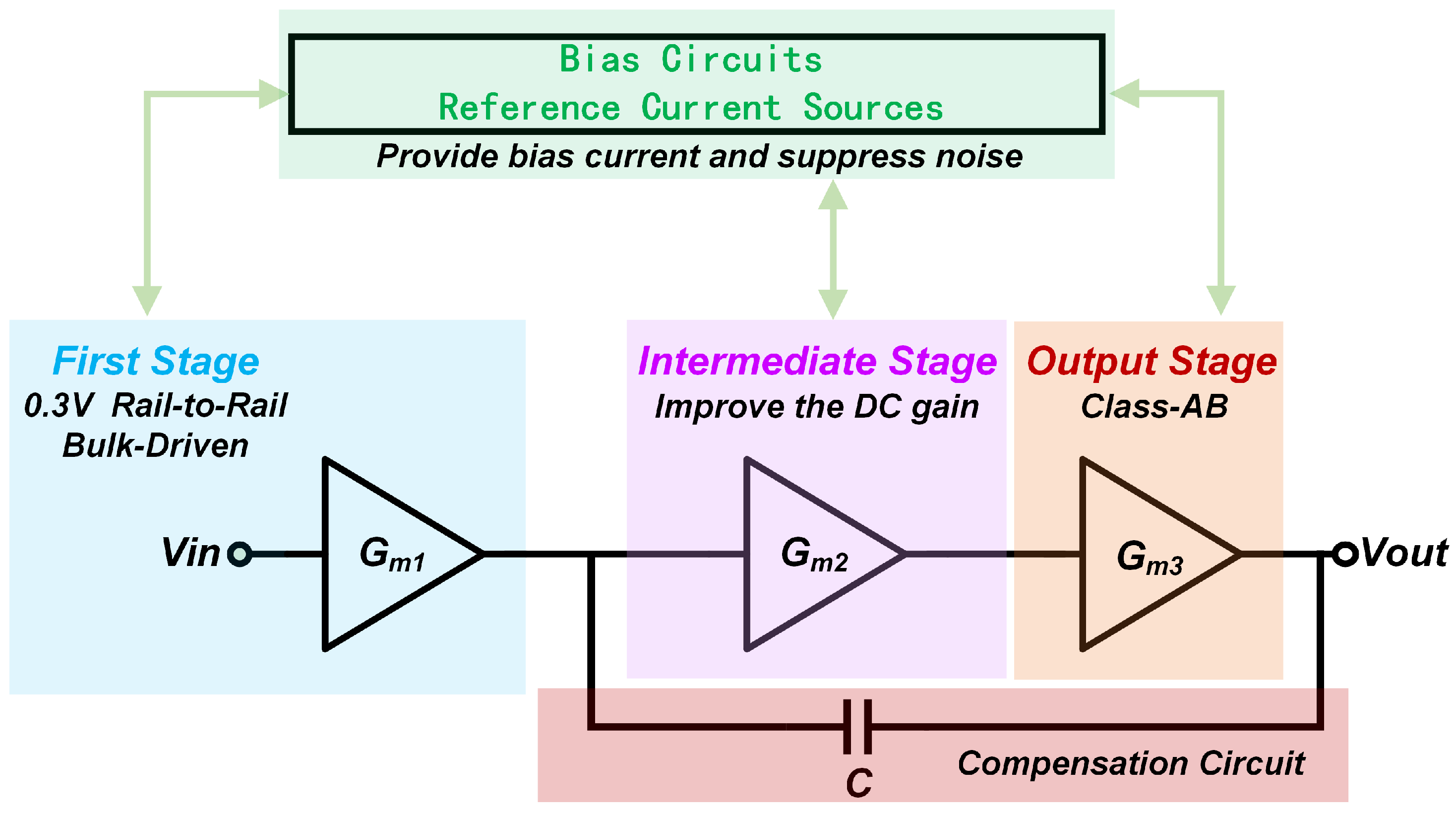
In terms of circuit architecture, the design adopts a carefully optimized three-stage structure. The input stage uses a bulk-driven differential pair. While achieving ultra-low voltage operation, it extends the input common-mode range through proper substrate biasing design, reaching complete rail-to-rail input capability. The introduction of an intermediate gain stage effectively boosts the overall gain without significantly increasing power consumption, providing necessary amplification capability for processing weak bioelectrical signals. The output stage employs a class-AB push-pull structure [16,17,18,19,20]. It not only achieves rail-to-rail output capability but also significantly improves load driving capability through the adaptive characteristics of the HABRtR technique. This ensures high efficiency and low distortion when driving subsequent circuits. To guarantee the stability of the three-stage structure, a dedicated frequency compensation network is designed to ensure stable operation under various working conditions [21,22,23,24].
The design characteristics of this amplifier are highly compatible with the requirements of wearable health monitoring systems. The 0.3 V ultra-low voltage operation capability makes it compatible with energy harvesting systems and miniature battery power supplies. The 123 nW ultra-low power consumption ensures the possibility of long-term continuous monitoring. The high gain and sufficient bandwidth brought by the HABRtR technique meet the requirements for precise amplification of weak biological signals. The complete rail-to-rail input-output capability maximizes the utilization of limited voltage swing, improving dynamic range and signal-to-noise ratio [25,26]. These characteristics make the proposed amplifier an ideal choice for wearable health monitoring applications, providing critical technical support for achieving long-term, reliable, and high-precision physiological parameter monitoring. Based on these innovative bulk-driven technologies, this paper presents a novel three-stage, ultra-low-voltage, and ultra-low-power rail-to-rail operational amplifier whose overall architecture is illustrated comprehensively in Figure 2 of the document.
The remainder of this paper systematically presents a detailed discussion of the proposed amplifier. Section 2 provides an in-depth introduction to the design principles and implementation methods of the ultra-low-voltage ultra-low-power rail-to-rail operational amplifier, including the overall three-stage architecture design, the gain and bandwidth optimized intermediate stage, the class-AB rail-to-rail output stage, and the frequency compensation technique for the multi-stage structure. Section 3 presents the implementation and simulation verification results of the amplifier. Through comprehensive performance metric testing and stability analysis, the reliability and practicality of the design are validated. Finally, Section 4 summarizes the main contributions of this research, analyzes the limitations of the current design, and discusses future research directions.

2. Overview of the Proposed OTA

2.1. Overall Circuit

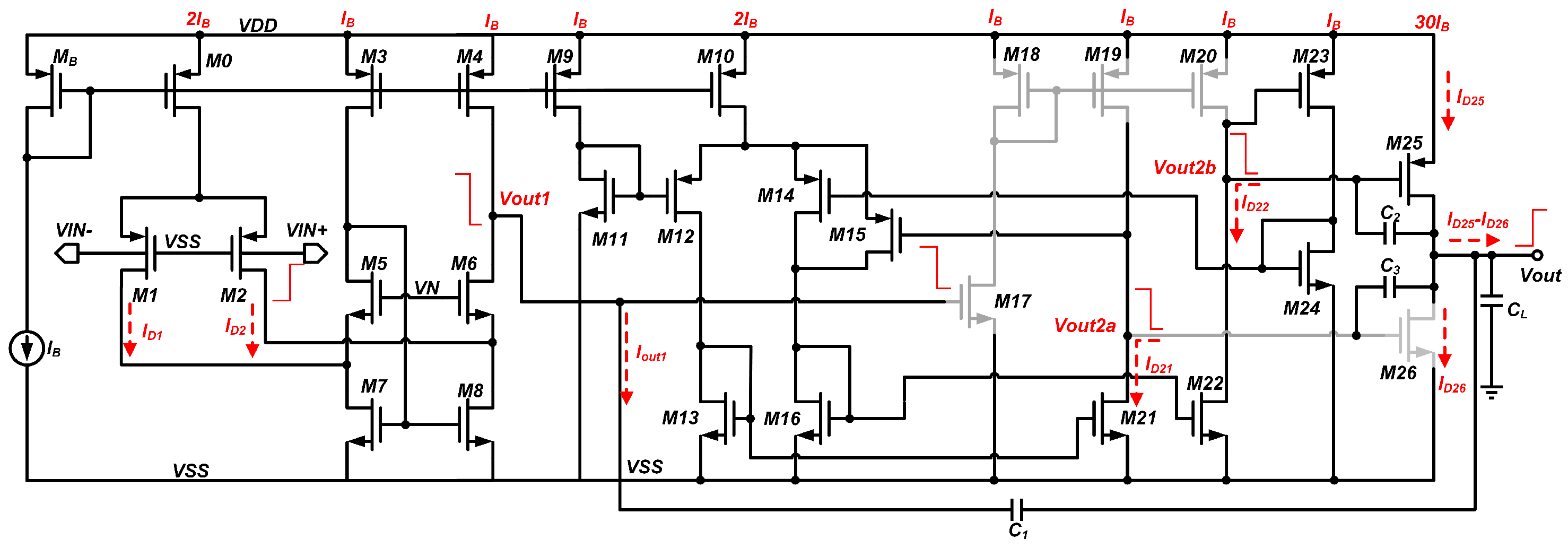
Figure 3 shows the overall circuit of the OTA.The overall structure of the operational amplifier is divided into three stages. M0–M8 form the input stage using bulk-driven technology, which can achieve rail-to-rail input. The intermediate stage consists of M17–M22 and is mainly used to increase the gain. M25 and M26 form a Class-AB push-pull output structure, which is used to achieve rail-to-rail output. M9–M15 and M23–M24 serve as the bias circuit for the Class-AB output stage to control the bias current of the output stage. In addition, the reference current source provides the static current I B for the core working circuit, and capacitors C 1 C 3 are the Miller capacitors of the operational amplifier for frequency compensation. All transistors are operating in the subthreshold region by design, and the architecture is optimized to ensure saturation even with VDD = 0.3 V across all corners.

2.2. The Bulk-Driven Input Stage

The overall structure of the input stage is a folded cascode amplifier. M1 and M2 are two PMOS differential input pair transistors using bulk-driven technology. M5–M8 form the cascode output stage. M0 is the tail current source of the input differential pair transistors, and M3 and M4 provide bias currents for the cascode output stage. The input signal is input from the bulk terminals of M1 and M2, and the gate terminals of the two input transistors are connected to the low-level VSS of the circuit. The bias voltage V N of M5 and M6 is provided by the bias circuit.
Due to the depletion-type characteristics of bulk-driven MOS transistors, the effect of the threshold voltage ( V T H ) on the input differential pair can be considered negligible. Therefore, for the input stage adopted in this paper, the maximum value of the common-mode input voltage is:
V C M , b d max = V D D V B S 1 , 2 + V D S A T 0
where V B S 1 , 2 is the bulk voltage of input differential pair M1 or M2, V d s a t 0 is the overdrive voltage of tail current source transistor M0. V B S 1 , 2 can be a positive value, which allows V C M , max to reach the supply voltage VDD. If M1 and M2 are traditional gate-driven differential pair, the maximum value of the input common-mode voltage at this time is:
V C M , g d max = V D D V D S A T 0 V T H 1 , 2
Compared to gate-driven differential pairs, bulk-driven differential pairs offer an increased input common-mode range due to the reduction in threshold voltage, significantly extending the differential pair’s common-mode input range. It is worth noting that when the bulk-source junction is excessively forward-biased, the internal parasitic horizontal and vertical BJTs will turn on, causing the bulk current to increase exponentially and making the parasitic lateral BJT dominant. Therefore, the magnitude of common-mode voltage V C M must be carefully considered in circuit design. However, for the circuit designed in this paper, operating under a 0.3 V supply voltage cannot generate sufficient voltage to excessively forward-bias the bulk-source junction, thus effectively avoiding the occurrence of self-parasitic effects.

2.3. Intermediate Stage and Output Stage

To achieve rail-to-rail output of the signal, a Class-AB output structure is adopted in this paper. Since the output stage is associated with the intermediate stage, for the convenience of analyzing its working principle, the two stages are analyzed together.
The intermediate stage circuit is a common-source circuit with a current mirror as the load. To meet the design requirements of ultra-low-voltage and ultra-low-power consumption, a simplified circuit architecture with a minimal number of transistor stages was adopted. Therefore, the common-source configuration is chosen as the second stage of the amplifier. Additionally, to further increase the gain, a current mirror is selected as the load. Considering the choice of the output stage, the second-stage amplifier is designed with two outputs. The voltage signal is converted into a current signal through the action of the common-source transistor M17, and then converted back into a voltage signal through the current mirror loads M18–M19 (M18–M20). M21 and M22 provide bias currents for the two output branches, and their bias voltages are connected to the feedback amplifier that controls the push-pull output of the third stage.
The quiescent current of the output stage is controlled as follows: A quiescent current I 1 is provided to M11, it generates a voltage V r e f . The sizes of M14 and M15 are half of M12, and both transistors are in parallel, making them equivalent to a single transistor of the same size as M12. The following relationship holds:
V ref = V G 14 = V G 15 = V G 26
From (3), the gate voltage of M24 is equal to the gate voltage of M11. Therefore, M26 can form a current mirror with M11, and the quiescent current flowing through M26 as follows:
I D 26 = ( W / L ) 26 ( W / L ) 11 I 1
Since the two branches of the amplifier in the biasing circuit are symmetrical, the currents flowing through the two branches are respective:
I D 14 = I D 12 = 1 2 I 2
M21 and M22 respectively form two current mirrors with M13 and M16, so the current flowing through M19 and M20 is 1 2 I 2 , and the quiescent current of M18 is also 1 2 I 2 . At this point, by setting the size of M23 so that V A = V B , the gate voltage of the output transistor M25 can be equal to the gate voltage of M18, and the quiescent current flowing through M25 can be obtained by mirroring M18.
I D 25 = ( W / L ) 25 ( W / L ) 18 I D 14 = 1 2 ( W / L ) 25 ( W / L ) 18 I 2
When I 2 is set to be 2 I 1 , the quiescent currents of the output PMOS and NMOS transistors will be equal. Therefore, the output stage transistors maintain a stable quiescent operating point, unaffected by the input common-mode voltage.With a unit quiescent current I B of 10 nA, the total quiescent current of the OTA is 410 nA, ensuring very low power consumption.

2.4. Small-Signal Analysis

Figure 4 presents the small-signal equivalent schematic of OTA, with C 1 , C 2 and C 3 serving as the compensating capacitors. The blue shaded area represents the feedback path of the Class-AB output stage control circuit. R O 1 , C O 1 , R O 2 , and C O 2 denote the output resistance and capacitor of the first and second stages of the OTA, respectively. R L and C L represent the load resistance and capacitor.
To calculate the transfer function of the OTA, the following premises should first be established: The C L and the compensation capacitors are much larger than the C O 1 and C O 2 . In the circuit design, the output stage is sized significantly larger, implying g m 3 g m 2 . Based on these conditions, we can simplify the formula for the amplifier’s transfer function to:
H ( s ) = g m b 2 g m 17 g m 25 + g m 26 R O 1 R O 2 R L 1 + s C 1 g m 17 g m 25 + g m 26 R O 1 R O 2 R L 1 + s C 2 + C 3 g m 17 + s 2 C L C 2 + C 3 g m 17 g m 25 + g m 26
According to (7), the amplifier has three poles, which are:
p 1 = p 3 d B = 1 C 1 g m 17 g m 25 + g m 26 R O 1 R O 2 R L
p 2 , 3 = g m 25 + g m 26 2 C L ± j g m 25 + g m 26 2 C L
p 1 is the dominant pole, while p 2 and p 3 are the two sub-dominant poles. From (8) and (9), it can be observed that the two sub-dominant poles of the amplifier are located far away from the dominant pole. The Miller capacitor shifts them outside the bandwidth, ensuring the stability of the system. The DC gain of the OTA can be derived as:
A D C = g m b 2 g m 17 g m 25 + g m 26 R O 1 R O 2 R L

2.5. Large-Signal Analysis

Since the input transistors M1 and M2 are bulk-driven MOS transistors, which are depletion-type devices, M1 and M2 are in a continuously conducting state. Moreover, the relationship between the current and the input voltage is opposite to that of gate-driven transistors. That is, the larger the input voltage, the greater the current flowing through them.Assuming a positive step signal is applied to VIN+, its charging process is shown in Figure 5.
When V i n + > V i n , the current I D 2 flowing through M2 is greater than the current I D 1 flowing through M1. At this time, capacitor C 1 is charged, and the slew rate limit of the first stage is:
S R 1 + = I D 2 I D 1 max C 1
Since the current of M6 increases, the output voltage V o u t 1 of the first stage drops. In the extreme case, M17 is turned off, and simultaneously M18, M19, and M20 are all turned off accordingly. Therefore, the output current I o u t 2 of the second stage is determined by I D 21 and I D 22 . The two compensation capacitors C 2 and C 3 discharge to M21 and M22 respectively. Thus, the slew rate limit of the second stage is:
S R 2 + = I D 19 , 20 C 2 , 3
During the decrease of V o u t 1 , V o u t 2 a and V o u t 2 b decrease simultaneously. At this time, the current flowing through the output transistor M25 increases, and the current flowing through M26 decreases. The output current charges C 1 , C 2 , C 3 , and C L simultaneously. In the extreme case, M26 will be turned off, and the slew rate limit of the third stage is:
S R 3 + = I D 23 I D 24 max C 1 + C 2 + C 3 + C L
The positive slew rate of the OTA is:
S R + = S R 1 + , S R 2 + , S R 3 + m i n
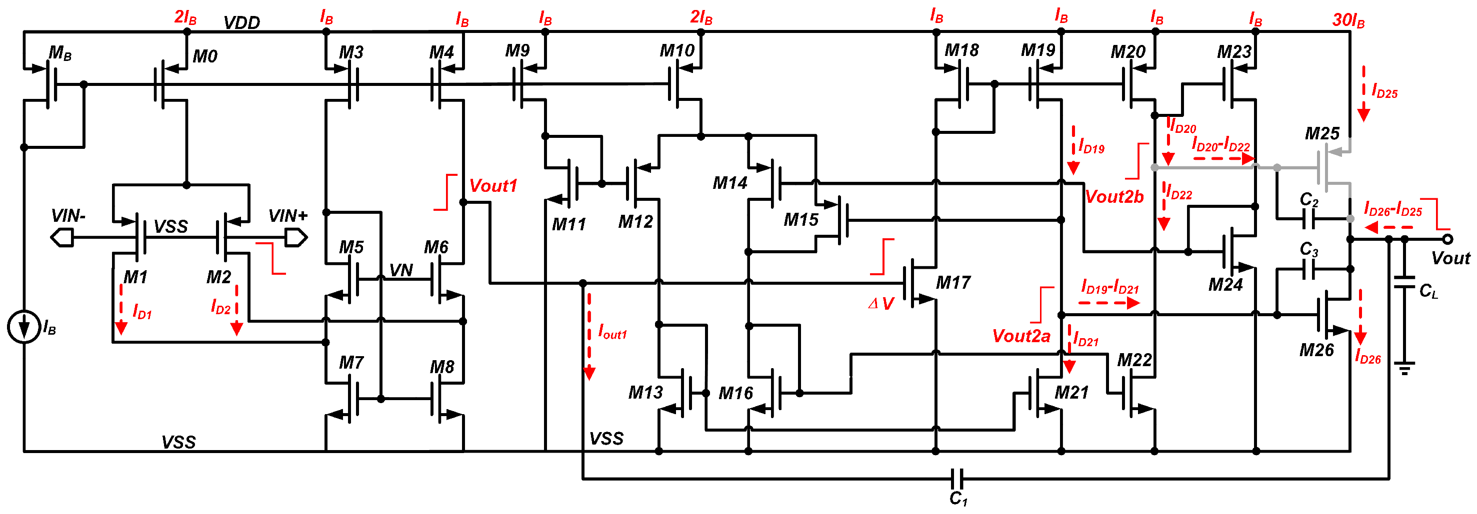
Assume that a negative step signal is applied to VIN+. The discharging process is shown in the Figure 6 as follows:
When V i n + < V i n , the current I D 2 flowing through M2 is less than the current I D 1 flowing through M1. At this time, capacitor C 1 is charged, and the slew rate limit of the first stage is:
S R 1 = I D 1 I D 2 max C 1
Since the current of M6 decreases, the output voltage V o u t 1 of the first stage increases by Δ V. To characterize the subthreshold conduction behavior of M17 (a bulk-driven MOS transistor operating in the subthreshold region), we introduce the subthreshold slope factor ζ (dimensionless) — a parameter accounting for non-ideal effects in subthreshold current. ζ is defined as ζ = 1 + C B S C O X , where C B S denotes the bulk-source junction capacitance of the MOS transistor, and C O X denotes the gate-oxide capacitance per unit area. For the SMIC 0.18 μ m CMOS process used in this design, the typical value of ζ for bulk-driven PMOS transistors (e.g., M17) is 1.2–1.3, consistent with process model data and industry-reported characteristics of subthreshold bulk-driven devices. A current will be generated through M17:
I D 17 = W L 17 I D 0 exp Δ V ζ ( k T / q )
The current I D 17 is replicated to I D 19 and I D 20 through the current mirror. The two output currents I o u t 2 charge C 2 and C 3 respectively. So, the slew rate limit of the second stage is:
S R 2 = W L 15 I D 0 exp Δ V ζ ( k T / q ) I D 19 , 20 C 2 , 3
During the rise of V o u t 1 , V o u t 2 a and V o u t 2 b rise simultaneously. At this time, the current flowing through the output transistor M26 increases, and the current flowing through M25 decreases. Capacitors C 1 , C 2 , C 3 , and C L discharge simultaneously. In the extreme case, M25 will be turned off, and the slew rate limit of the third stage is:
S R 3 = I D 24 I D 23 max C 1 + C 2 + C 3 + C L
The negative slew rate of the OTA is:
S R = S R 1 , S R 2 , S R 3 min

3. Simulation and Experimental Results

3.1. Simulation Results

The OTA was designed using a standard SMIC 0.18 μ m CMOS technology. Some results of preliminary simulations are discussed in this section. Table 1 shows the W/L ratios of all transistors. In addition, the capacitance value of C 1 is 40.69 fF, while the capacitance values of C 2 and C 3 are both 5.17 fF. In Figure 3, the bias current I B is 10 nA.
First, the rail-to-rail input and output performance of the amplifier is verified through simulation. Figure 7a shows the simulation results of the input common-mode voltage of the amplifier under the TT process corner and at room temperature. The blue curve represents the relationship between the output voltage and the input voltage, and the orange curve represents the slope of the input-output curve. It can be concluded that the input common-mode voltage range of the amplifier is from 2.25 mV to 298.5 mV, which can meet the rail-to-rail input performance under the TT process corner and at room temperature. Figure 7b shows the simulation results of the output voltage swing under the TT process corner, which is from 4.27 mV to 299.7 mV, basically meeting the requirements of the rail-to-rail output range.
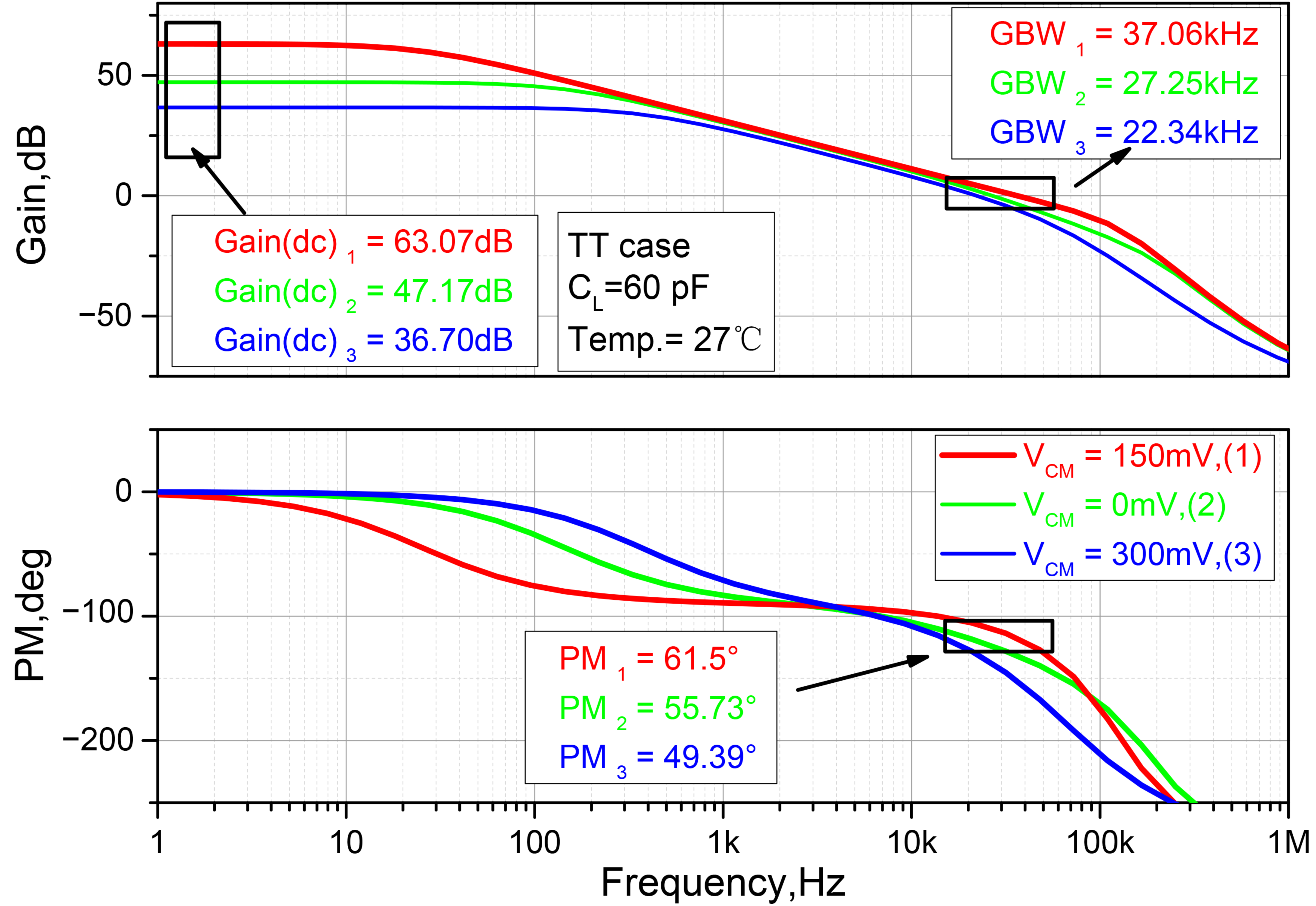
The AC frequency characteristics of the OTA, including the amplitude-frequency characteristic and the phase-frequency characteristic, are one of the most basic parameters of the amplifier. The simulation results of these characteristics under the TT process corner are shown in Figure 8. For a common-mode input voltage ( V cm ) of 150 mV, the DC gain of the amplifier is 63.07 dB, the phase margin is 61.5°, and the unity-gain bandwidth product is 37.06 kHz. The performance varies as V cm changes. When V cm = 0 V, the DC gain is 47.17 dB, the phase margin is 55.73°, and the unity-gain bandwidth product is 27.25 kHz. Furthermore, for V cm = 300 mV, the DC gain becomes 36.70 dB, with a phase margin of 49.39° and a unity-gain bandwidth product of 22.34 kHz.
The common-mode rejection ratio (CMRR) reflects the amplifier’s ability to amplify differential-mode signals and suppress common-mode interference signals. The simulation results are shown in Figure 9a, and the CMRR is 69.89 dB. The power-supply rejection ratio (PSRR) reflects the degree to which the output voltage is affected by the change in the power-supply voltage. The simulation results are shown in Figure 9b, and the PSRR is 69.89 dB. The PSRR of the proposed amplifier reflects a deliberate design trade-off, prioritizing ultra-low-power consumption and a competitive GBW product. To achieve these design goals, the simplified intermediate stage, optimized for low power, omits the cascode load structure (cf. [24]), which typically enhances power-supply noise suppression. Additionally, the Class-AB output stage employs a minimal 10 nA bias current to reduce static power, thereby influencing the circuit’s ability to reject power-supply fluctuations.
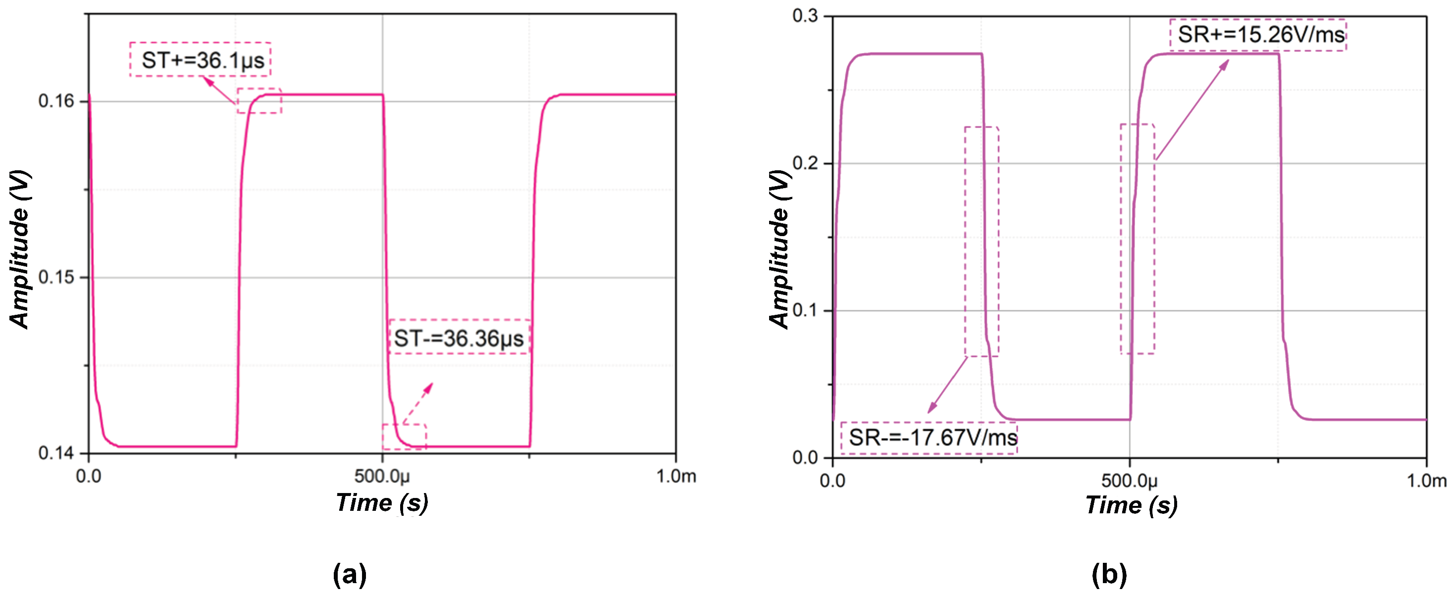
The settling time is an important parameter for measuring the small-signal transient response of the amplifier. As can be seen from Figure 10a, the rising settling time ST+ is 36.1 μ s, and the falling settling time ST- is 36.36 μ s. When the input signal is a square wave with a small peak-to-peak value, the output signal of the amplifier is normal under the typical process corner. The slew rate is used to measure the large-signal transient performance of the amplifier, and its simulation results are shown in Figure 10b.
Simulation result for the noise performance is shown in Figure 11. Note that the thermal noise at Vcm = 150 mV (10 KHz) is 872 nV / Hz . This performance supports the suitability of this OTA for low-noise analog front-end applications such as biomedical signal processing.
At the end of this section, Table 2 presents detailed simulation results across TT, FF, and SS corners under multiple temperatures. The OTA demonstrates strong robustness to PVT variations. The DC gain remains above 45 dB in all cases, with a typical value of 63.07 dB at TT/27 °C. Even under the extreme FF/50 °C condition, the gain degradation to 25.8 dB is tolerable due to reduced output impedance and transconductance, as expected in fast corners. Importantly, the phase margin maintains stability across most corners, ranging from 47.42° to 80.3°, except for a marginal case of −9.87° under FF/−40 °C, which can be improved with tuning of compensation capacitors.The common-mode input range consistently covers over 98% of the supply voltage range, e.g., 2.25–298.5 mV in TT/27 °C, validating the effectiveness of the bulk-driven input stage. Similarly, the output swing extends near rail-to-rail across all corners, indicating successful Class-AB output design. Notably, the OTA maintains functional slew rate even in SS/50 °C (16.58/−14.63 V/ms), while reaching up to 61.69 V/ms in FF/−40 °C. This wide SR variation aligns with bias current scaling under temperature and process extremes. The CMRR consistently exceeds 40 dB across corners, with a peak of 69.89 dB in TT/27 °C, ensuring strong differential-mode selectivity. PSRR, though lower due to 0.3V VDD limitations, achieves a maximum of 57.34 dB, and remains within acceptable bounds for low-voltage OTA designs. These results together affirm the circuits resilience and performance stability under realistic environmental variations.

3.2. Experimental Results

Based on the SMIC 0.18 μ m process, this paper completed the chip tape-out, and the final chip layout and micrograph are shown in the Figure 12.
When measuring the output voltage swing, the input signal was set as a sinusoidal wave with a peak-to-peak value of 300 m V p p and a frequency of 1 kHz. As shown in Figure 13, the output voltage swing of the amplifier reaches 290.5 mV, meeting the rail-to-rail requirement.
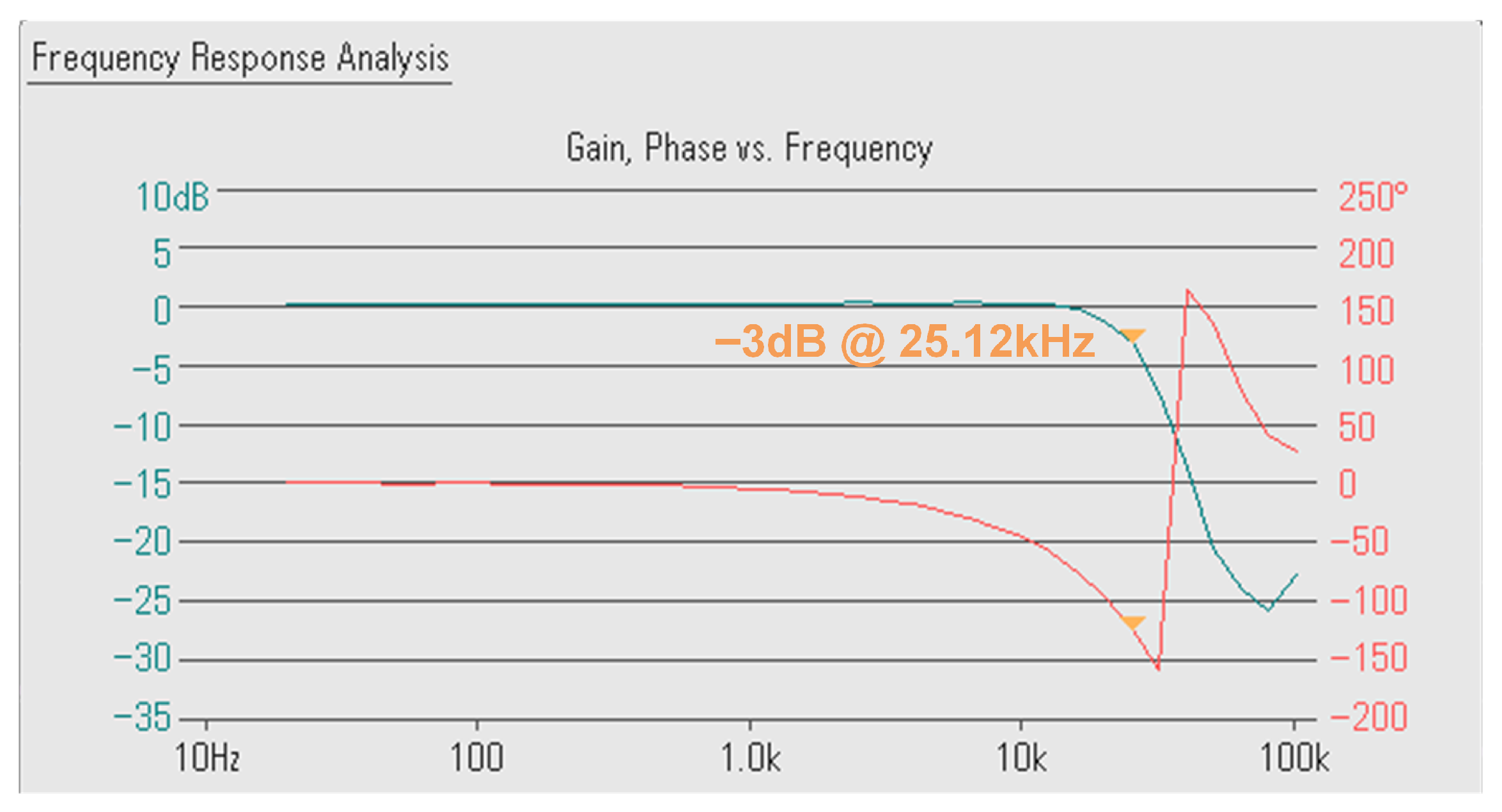
The GBW measurement setup is shown in Figure 14, which is used to verify the theoretical results. The proposed OTA is configured as unity-gain inverting amplifier and the feedback coefficient of this closed loop is 0.75. A Keysight EDUX1002G digital storage oscilloscope is used to supply the input AC signal and capture the input and output. In this measurement circuit. The measured closed-loop AC response of EFC-OTA is shown in Figure 15. It is clear that the 3 dB bandwidth of this closed loop is 25.12 kHz. Hence the GBW of EFC-OTA is 37.68 kHz, which approximately agrees with the simulation result of 37.06 kHz.
The Figure 16 and Figure 17 respectively show the large-signal and small-signal transient responses. When measuring the large-signal transient response and slew rate of the amplifier, a 250 m V p p , 1 kHz square wave signal was used as the input. The measured rising slew rate SR+ is 19.4 V/ms, and the falling slew rate SR− is 24.3 V/ms, with no obvious oscillation in the signal. A 50 m V p p , 1 kHz square wave signal was used to measure the small-signal transient response and settling time, resulting in a rising settling time ST+ of 36 μ s and a falling settling time ST− of 32.4 μ s. Additionally, there is slight overshoot in the small-signal transient response.
Figure 18 shows the Monte Carlo simulation results for the OTA. The results indicate that key metrics such as DC gain and GBW exhibit a reasonable distribution, ensuring that the OTA’s performance remains relatively consistent under process variations.
As shown in Table 3, the proposed design is benchmarked against several state-of-the-art ultra-low voltage OTAs published from 2018 to 2024. Despite being implemented in the mature 180 nm process, this work achieves highly competitive performance.The proposed OTA consumes only 123 nW with a 60 pF load, representing a balanced trade-off between power and capacitive driving capability. This is significantly lower than many designs such as [22,26], showing superior current efficiency. The measured GBW of 37.68 kHz is the highest among all 0.3 V OTAs in the comparison, and the SR of 21.85 V/ms is competitive even against designs operating at higher power (e.g., [27] at 21.6 V/ms with 73 nW). These improvements are attributed to the Class-AB output stage with enhanced drive capability and minimal static bias current. The OTA achieves a DC gain of 63.07 dB, comparable to [28,29], and an exceptional CMRR of 69.89 dB, which surpasses many designs using advanced process nodes or more complex topologies. The small-signal figure of merit FoMS reaches 12.25 MHz·pF/μW, and the large-signal FoML reaches 10.66 V/μs·pF/μW, both outperforming most other works. These FoMs confirm that the proposed design offers an optimal balance of speed, power, and load-driving capability.
A Monte Carlo simulation (500 iterations) was conducted to assess the proposed amplifier’s process variation robustness: key metrics showed tight, stable distributions—with a mean DC gain of 63.02 dB, GBW of 37.12 kHz. Results are showed in Figure 18. All parameters clustered around their nominal values, confirming the amplifier’s consistent performance across process fluctuations, which suits its application in low-voltage wearable health monitoring systems.

4. Conclusions

This paper presents a high-efficiency, ultra-low-voltage OTA that operates at 0.3 V and features rail-to-rail input/output capabilities with enhanced GBW and SR. The design employs a bulk-driven technique in the input stage to extend the common-mode input range under subthreshold conditions and overcome the threshold voltage limitations of conventional gate-driven MOS transistors. A simplified intermediate stage is implemented to ensure low-power operation while preserving normal transistor functionality at ultra-low-voltages. Additionally, a modified Class-AB control loop in the output stage stabilizes the quiescent current and minimizes power consumption, thereby achieving efficient rail-to-rail output. Fabricated using SMIC 0.18 μ m technology, the OTA exhibits outstanding performance: under a 0.3 V supply and a 60 pF load, it consumes only 123 nW, attaining nanowatt-level power efficiency. Key measured results include a DC gain of 63.07 dB, a phase margin of 61.5°, an experimental GBW of 37.68 kHz, and a slew rate of 21.85 V/ms. The amplifier also demonstrates superior figures of merit (FoM), with a small-signal FoMS of 12.25 MHz·pF/ μ W and a large-signal FoML of 10.66 V/ μ s·pF/ μ W, thereby outperforming many state-of-the-art low-voltage OTAs in terms of efficiency and speed. Comparative analysis with recent works underscores the design’s balanced trade-offs of low power, wide bandwidth, and high slew rate, making it highly suitable for energy-constrained applications such as portable electronics, IoT sensors, and biomedical devices. Although the PSRR is relatively modest due to the ultra-low-voltage limitations, the OTA’s overall performance establishes a new benchmark for high-efficiency, rail-to-rail operation in sub-0.5 V regimes. Future work may focus on further enhancements in PSRR and on integrating the design with advanced low-power circuits to broaden its applicability in ultra-low-voltage systems.

Author Contributions

Conceptualization, Y.W. and J.Z.; Investigation, Y.W. and S.Z.; Formal analysis, J.Z. and H.Z.; Methodology, Q.Z. and S.Z.; Writing-original draft preparation, Y.W. and S.Z.; Writing—review and editing, Q.Z. and J.Z. All authors have read and agreed to the published version of the manuscript.

Funding

This research is supported by the National Science and Technology Major Project for Deep Earth Probe and Mineral Resources Exploration (2024ZD1002700), the National Natural Science Foundation of China (Grant No. 42074155), the Fundamental Research Funds for the Central Universities, China University of Geosciences Beijing (Grant No. 2-9-2023-011) and the Key Research Program of the Chinese Academy of Sciences (Grant No. KGFZD-145-22-06-02).

Institutional Review Board Statement

Not applicable.

Informed Consent Statement

Not applicable.

Data Availability Statement

Data are contained within the article.

Conflicts of Interest

The authors declare no conflict of interest.

References

  1. Jacob Rodrigues, M.; Postolache, O.; Cercas, F. Physiological and behavior monitoring systems for smart healthcare environments: A review. Sensors 2020, 20, 2186. [Google Scholar] [CrossRef]
  2. Ghasemzadeh, H.; Jafari, R. Ultra low-power signal processing in wearable monitoring systems: A tiered screening architecture with optimal bit resolution. ACM Trans. Embed. Comput. Syst. 2013, 13, 1–23. [Google Scholar] [CrossRef]
  3. He, T.; Lee, C. Evolving flexible sensors, wearable and implantable technologies towards bodyNET for advanced healthcare and reinforced life quality. IEEE Open J. Circuits Syst. 2021, 2, 702–720. [Google Scholar] [CrossRef]
  4. Abdelfattah, O.; Roberts, G.W.; Shih, I.; Shih, Y.C. An ultra-low-voltage CMOS process-insensitive self-biased OTA with rail-to-rail input range. IEEE Trans. Circuits Syst. I Regul. Pap. 2015, 62, 2380–2390. [Google Scholar] [CrossRef]
  5. Das, R.; Moradi, F.; Heidari, H. Biointegrated and wirelessly powered implantable brain devices: A review. IEEE Trans. Biomed. Circuits Syst. 2020, 14, 343–358. [Google Scholar] [CrossRef]
  6. Xu, W.; Wang, T.; Wei, X.; Yue, H.; Wei, B.; Duan, J.; Li, H. Low noise, high input impedance digital-analog hybrid offset suppression amplifier for wearable dry electrode ECG monitoring. Electronics 2020, 9, 165. [Google Scholar] [CrossRef]
  7. Qin, Z.; Tanaka, A.; Takaya, N.; Yoshizawa, H. 0.5-V 70-nW Rail-to-rail operational amplifier using a cross-coupled output stage. IEEE Trans. Circuits Syst. II Express Briefs 2016, 63, 1009–1013. [Google Scholar] [CrossRef]
  8. Horestani, F.K.; Eshghi, M.; Yazdchi, M. An ultra-low power amplifier for wearable and implantable electronic devices. Microelectron. Eng. 2019, 216, 111054. [Google Scholar] [CrossRef]
  9. Duch, L.; Basu, S.; Braojos, R.; Ansaloni, G.; Pozzi, L.; Atienza, D. HEAL-WEAR: An Ultra-Low Power Heterogeneous System for Bio-Signal Analysis. IEEE Trans. Circuits Syst. I Regul. Pap. 2017, 64, 2448–2461. [Google Scholar] [CrossRef]
  10. Xu, J.; Qu, T.; Pan, Q.; Li, Y.; Liu, L.; Li, Y.; Zhou, J.; Yao, C.; Hong, Z. Analog Front-End Circuit Techniques for Wearable ExG, BioZ, and PPG Signal Acquisition: A Review. IEEE Open J.-Solid-State Circuits Soc. 2025, 5, 251–268. [Google Scholar] [CrossRef]
  11. Grasso, A.D.; Marano, D.; Palumbo, G.; Pennisi, S. Design methodology of subthreshold three-stage CMOS OTAs suitable for ultra-low-power low-area and high driving capability. IEEE Trans. Circuits Syst. I Regul. Pap. 2015, 62, 1453–1462. [Google Scholar] [CrossRef]
  12. Grasso, A.D.; Pennisi, S. Ultra-low power amplifiers for IoT nodes. In Proceedings of the 2018 25th IEEE International Conference on Electronics, Circuits and Systems (ICECS), Bordeaux, France, 9–12 December 2018; pp. 497–500. [Google Scholar]
  13. Chatterjee, S.; Tsividis, Y.; Kinget, P. Ultra-low voltage analog integrated circuits. IEICE Trans. Electron. 2006, 89, 673–680. [Google Scholar] [CrossRef]
  14. Naderi, M.H.; Park, C.; Prakash, S.; Kinyua, M.; Soenen, E.G.; Silva-Martinez, J. A 27.7 fJ/conv-step 500 MS/s 12-bit pipelined ADC employing a sub-ADC forecasting technique and low-power class AB slew boosted amplifiers. IEEE Trans. Circuits Syst. I Regul. Pap. 2019, 66, 3352–3364. [Google Scholar] [CrossRef]
  15. Gagliardi, F.; Catania, A.; Piotto, M.; Bruschi, P.; Dei, M. Parallel Slew-Rate Enhancer With Current-Recycling Core for Switched-Capacitors Circuits. IEEE Trans. Circuits Syst. II Express Briefs 2024, 71, 4814–4818. [Google Scholar] [CrossRef]
  16. Ballo, A.; Grasso, A.D.; Pennisi, S. 0.4-V, 81.3-nA bulk-driven single-stage CMOS OTA with enhanced transconductance. Electronics 2022, 11, 2704. [Google Scholar] [CrossRef]
  17. Khateb, F.; Kumngern, M.; Kulej, T.; Biolek, D. 0.5 V Differential difference transconductance amplifier and its application in voltage-mode universal filter. IEEE Access 2022, 10, 43209–43220. [Google Scholar] [CrossRef]
  18. Centurelli, F.; Della Sala, R.; Monsurro, P.; Tommasino, P.; Trifiletti, A. An ultra-low-voltage class-AB OTA exploiting local CMFB and body-to-gate interface. AEU-Int. J. Electron. Commun. 2022, 145, 154081. [Google Scholar] [CrossRef]
  19. Akbari, M.; Hussein, S.M.; Hashim, Y.; Tang, K.T. 0.4-V Tail-less quasi-two-stage OTA using a novel self-biasing transconductance cell. IEEE Trans. Circuits Syst. I Regul. Pap. 2022, 69, 2805–2818. [Google Scholar] [CrossRef]
  20. Kulej, T.; Khateb, F.; Arbet, D.; Stopjakova, V. A 0.3-V high linear rail-to-rail bulk-driven OTA in 0.13 μm CMOS. IEEE Trans. Circuits Syst. II Express Briefs 2022, 69, 2046–2050. [Google Scholar] [CrossRef]
  21. Woo, K.C.; Yang, B.D. A 0.25-V rail-to-rail three-stage OTA with an enhanced DC gain. IEEE Trans. Circuits Syst. II Express Briefs 2019, 67, 1179–1183. [Google Scholar] [CrossRef]
  22. Akbari, M.; Hussein, S.M.; Hashim, Y.; Tang, K.T. An enhanced input differential pair for low-voltage bulk-driven amplifiers. IEEE Trans. Very Large Scale Integr. Syst. 2021, 29, 1601–1611. [Google Scholar] [CrossRef]
  23. Della Sala, R.; Centurelli, F.; Scotti, G.; Tommasino, P.; Trifiletti, A. A differential-to-single-ended converter based on enhanced body-driven current mirrors targeting ultra-low-voltage OTAs. Electronics 2022, 11, 3838. [Google Scholar] [CrossRef]
  24. Della Sala, R.; Centurelli, F.; Monsurrò, P.; Scotti, G.; Trifiletti, A. A 0.3 V rail-to-rail three-stage OTA with high DC gain and improved robustness to PVT variations. IEEE Access 2023, 11, 19635–19644. [Google Scholar] [CrossRef]
  25. Ballo, A.; Grasso, A.D.D.; Pennisi, S.; Susinni, G. A 0.3-V 8.5-μ A bulk-driven OTA. IEEE Trans. Very Large Scale Integr. Syst. 2023, 31, 1444–1448. [Google Scholar] [CrossRef]
  26. Ballo, A.; Carvajal, R.G.; Grasso, A.D.; Luján-Martínez, C.I.; Pennisi, S.; Venezia, C. 0.35 V SR-enhanced bulk-driven OTA for loads up to 10 nF. IEEE Trans. Circuits Syst. I Regul. Pap. 2024, 71, 6410–6418. [Google Scholar] [CrossRef]
  27. Centurelli, F.; Della Sala, R.; Monsurrò, P.; Scotti, G.; Trifiletti, A. A 0.3 V rail-to-rail ultra-low-power OTA with improved bandwidth and slew rate. J. Low Power Electron. Appl. 2021, 11, 19. [Google Scholar] [CrossRef]
  28. Kulej, T.; Khateb, F. Design and implementation of sub 0.5 V OTAs in 0.18-μm CMOS. Int. J. Circuit Theory Appl. 2018, 46, 1129–1143. [Google Scholar] [CrossRef]
  29. Kulej, T.; Khateb, F. A compact 0.3-V Class AB bulk-driven OTA. IEEE Trans. Very Large Scale Integr. Syst. 2019, 28, 224–232. [Google Scholar] [CrossRef]
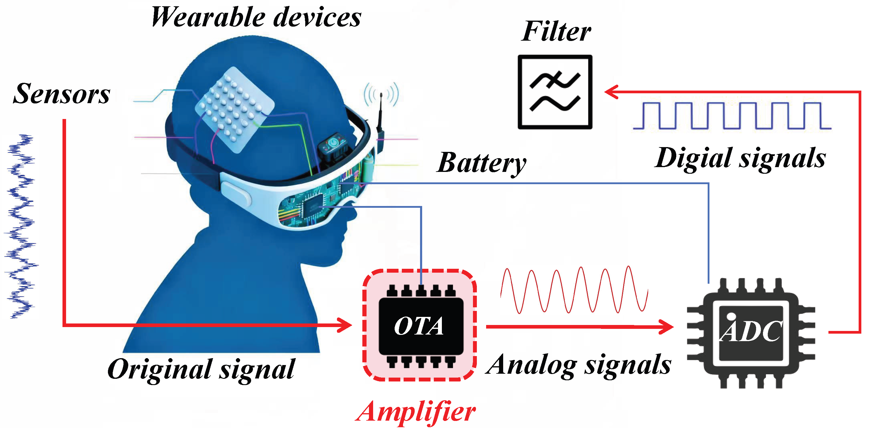
Figure 1. A typical wearable health monitoring system.
Electronics 14 04702 g001
Figure 2. Overall block diagram of the proposed OTA.
Electronics 14 04702 g002
Figure 3. Overall Circuit.
Electronics 14 04702 g003
Figure 4. Small-Signal Equivalent Schematic of OTA.
Electronics 14 04702 g004
Figure 5. Schematic diagram of the charging process when a positive step signal is applied at the V i n + terminal.
Electronics 14 04702 g005
Figure 6. Schematic diagram of the charging process when a negative step signal is applied at the V i n + terminal.
Electronics 14 04702 g006
Figure 7. Simulation results of (a) common-mode input voltage range and (b) output voltage swing.
Electronics 14 04702 g007
Figure 8. Simulated results of frequency response.
Electronics 14 04702 g008
Figure 9. Simulation results of (a) CMRR and (b) PSRR.
Electronics 14 04702 g009
Figure 10. Simulation results of (a) setting time and (b) slew rate.
Electronics 14 04702 g010
Figure 11. The noise performance of the proposed amplifier at Vcm = 150 mV.
Electronics 14 04702 g011
Figure 12. Microphotograph of the chip.
Electronics 14 04702 g012
Figure 13. Measured result of the output voltage swing.
Electronics 14 04702 g013
Figure 14. Test circuit for GBW.
Electronics 14 04702 g014
Figure 15. Measured results-AC frequency response.
Electronics 14 04702 g015
Figure 16. Measured results-large-signal transient response.
Electronics 14 04702 g016
Figure 17. Measured results-small-signal transient response.
Electronics 14 04702 g017
Figure 18. Monte carlo simulation results.
Electronics 14 04702 g018
Table 1. W/L of all transistors.
MOSFETW/L( μ m/ μ m)MOSFETW/L( μ m/ μ m)
M0, M3, M4, M9, M100.3/1M12, M14, M154/1
M1, M2, M18, M19, M200.5/1M13, M16, M21, M22, M243/1
M5, M63/0.9M170.7/1
M7, M81.8/1M23, M250.8/1
M115/1M265/1
Table 2. Main Performance Parameters of the Proposed Amplifier Across Process Corners and Temperature Range.
TTFFSS
Parameter −25 °C−27 °C−50 °C−25 °C−27 °C−50 °C−25 °C−27 °C−50 °C
ICMR (mV)5.45–299.72.25–298.521.4–271.310.2–299.76.9–25010.88–295.319.6–299.710–289.810.03–287.1
Swing (mV)2.65–272.44.27–299.770.73–291.61.41–294.153.56–296.254.51–296.715.42–296.45.18–296.713.52–296.7
DC gain (dB)69.3263.0745.9932.9828.3825.869.3267.1366.19
PM (°)57.261.571.4148.1380.365.242.1847.4254.64
GBW (kHz)48.4643.9120.997.629.958.235.0736.3738.64
CMRR (dB)75.0169.8926.3545.7241.4742.2550.3652.7965.74
PSRR (dB)30.1257.3415.0320.967.0115.119.9628.1120.82
ST ( μ s)42.95/47.8736.1/36.3654.44/53.7393.54/115.2496.72/11290.29/11045.16/40.2838.25/38.0540.36/39.31
SR (V/ms)20.89/−25.9518.22/−20.1111.42/−11.092.69/−2.64.65/−4.921.88/−24.9325.16/−13.7821.54/−14.9216.58/−14.63
Table 3. Performance comparison with existing low-voltage and low-power OTAs.
Ref.[28][29][22][27][23][24][26]This Work
Year2018202020212021202220232024 2025
Tech. (nm)18018018013013013065 180
Area ( mm 2 × 10 3 )8.28.5193.62.352.3452 13.77
Supply Voltage (V)0.30.30.50.30.30.30.35 0.3
Power (nW)15.412.645.57333.7333.73490 123
CL (pF)2030154025035300 60
DC gain (dB)65.864.77840.841.2886.8355 63.07
PM (deg)61525951.9358.2758.2765 61.5
GBW (kHz)2.782.967.518.657.9510.3215.4 37.68
CMRR (dB)72110113.867.4935.2857.858 69.89
PSRR (dB)625684.44574.4146.5926.5 57.34
SR (V/ms)7.124.158.621.61.253.7414 21.85
FoMS 13.617.0472.4710.216.56310.79.43 12.25
FoML 29.259.882.8411.822.6043.888.57 10.66
1  F o M S = G B W × C L power 2  F o M L = S R × C L power .
Disclaimer/Publisher’s Note: The statements, opinions and data contained in all publications are solely those of the individual author(s) and contributor(s) and not of MDPI and/or the editor(s). MDPI and/or the editor(s) disclaim responsibility for any injury to people or property resulting from any ideas, methods, instructions or products referred to in the content.