Article

Optimized Implementation of YOLOv3-Tiny for Real-Time Image and Video Recognition on FPGA

DII—Dipartimento di Ingegneria dell’Informazione, Università Politecnica delle Marche, Via Brecce Bianche 12, I-60131 Ancona, Italy
*
Author to whom correspondence should be addressed.
Electronics 2025, 14(20), 3993; https://doi.org/10.3390/electronics14203993
Submission received: 30 August 2025 / Revised: 3 October 2025 / Accepted: 9 October 2025 / Published: 12 October 2025

Abstract

In recent years, the demand for efficient neural networks in embedded contexts has grown, driven by the need for real-time inference with limited resources. While GPUs offer high performance, their size, power consumption, and cost often make them unsuitable for constrained or large-scale applications. FPGAs have therefore emerged as a promising alternative, combining reconfigurability, parallelism, and increasingly favorable cost–performance ratios. They are especially relevant in domains such as robotics, IoT, and autonomous drones, where rapid sensor fusion and low power consumption are critical. This work presents the full implementation of a neural network on a low-cost FPGA, targeting real-time image and video recognition for drone applications. The workflow included training and quantizing a YOLOv3-Tiny model with Brevitas and PyTorch, converting it into hardware logic using the FINN framework, and optimizing the hardware design to maximize use of the reprogrammable silicon area and inference time. A custom driver was also developed to allow the device to operate as a TPU. The resulting accelerator, deployed on a Xilinx Zynq-7020, could recognize 208 frames per second (FPS) when running at a 200 MHz clock frequency, while consuming only 2.55 W. Compared to Google’s Coral Edge TPU, the system offers similar inference speed with greater flexibility, and outperforms other FPGA-based approaches in the literature by a factor of three to seven in terms of FPS/W.

1. Introduction

The embedded ecosystem is extremely broad, ranging from small microcontrollers to complex systems capable of handling fairly significant computations. What distinguishes it from the desktop or server domain is not only the physical size of the devices but, above all, a set of constraints related to power consumption, thermal dissipation, cost, and, more generally, the need to operate under conditions often far removed from the controlled environment of a data center. In the embedded world, there is a frequent need for reliable devices with high operational availability that, at the same time, do not exceed certain power consumption or cost thresholds. One needs only to think of remote sensors distributed in areas without infrastructure, robots operating in harsh environments, or drones employed in activities requiring high flight autonomy.
For many years, the inference of advanced neural networks, such as object detection and recognition, was restricted to powerful servers or workstations equipped with GPUs [1]. However, the growing interest in applications that require on-site data processing, with low latency and without relying on a high-bandwidth connection, has highlighted the need for more flexible solutions. This is where the embedded world and artificial intelligence converge, giving rise to an entire field of research and development focused on algorithms and hardware architectures optimized for complex computations in limited space and under strict power constraints [2,3]. In these scenarios, the constraints imposed by the operating environment (limited-size batteries, minimal cooling requirements, competitive per-unit cost) represent concrete challenges that have driven technological innovation in various directions: from the design of SoCs with integrated accelerators (NPU) to dedicated processing units for neural networks (TPU) [4] and the use of FPGAs.
FPGAs are particularly attractive thanks to their reconfigurability, parallelism, and the possibility of deeply optimizing the inference pipeline by working at the hardware level and integrating quantized models that significantly reduce memory usage and the necessary bandwidth by using integer computation, rather than the much more standard floating point method [5].
Their advantages are especially evident in domains such as autonomous drones, where multiple heterogeneous sensors (IMU, cameras, proximity sensors, and GNSS) must be processed in real time. Local inference enables drones to reduce latency, improve autonomy, and operate in scenarios where remote connectivity is unreliable, such as search and rescue or agricultural monitoring [6,7]. At the same time, weight, power consumption, and heat dissipation impose strict design constraints, making GPU-based solutions impractical for small or energy-efficient platforms [8].
Having the ability to perform inference directly on board drones offers significant advantages. On the one hand, it eliminates or drastically reduces the dependence on a remote connection to send data to a server for processing. In critical scenarios, such as search and rescue missions in remote areas or inspection operations in regions with no stable network coverage, this on-board processing capability becomes essential to the success of the operation. On the other hand, latency times decrease because processing is carried out locally: the drone can make faster decisions without waiting for the response of a remote infrastructure. However, integrating an inference engine on board a drone adds further challenges related to payload weight, energy consumption (directly affecting battery life and thus flight autonomy), and the heat generated by any high-performance computing devices.
While dedicated GPU provide notable performance in the field of neural networks, they often become unsustainable for drones of reduced size or in any design aiming to keep weight and power consumption to a minimum. GPU-based solutions not only increase the overall cost of the vehicle but also require adequate cooling systems and power supplies, factors that can scale significantly if very high computational performance is targeted. Nonetheless, in many cases, on-board AI does not necessarily have to handle extremely large models: lighter neural networks [9,10], suitably quantized and optimized, are often more than enough for obstacle detection, object recognition, or target tracking, as long as a latency of a few milliseconds or a few tens of milliseconds is ensured.
In this context, lightweight and quantized neural networks [11], combined with FPGA acceleration, offer a promising path toward efficient on-board AI. Low-cost FPGA devices, though less powerful than high-end GPUs, can achieve competitive performance with significantly better energy efficiency and cost–performance ratios [12]. Thanks to the great flexibility offered by hardware-level reconfigurability and a high degree of parallelism, a well-designed FPGA can perform inference operations extremely efficiently, reducing memory bottlenecks and fully exploiting parallel pipelines for data processing. Moreover, in the case of drones intended for commercial or consumer activities, the availability of low-end FPGA—which are less expensive and have lower power consumption compared to high-end models—makes this technology even more appealing. These include certain devices that, while they may not compete with high-end GPU in terms of sheer power, offer a significant advantage in terms of energy efficiency and performance/cost ratio.
The presence of an inference engine on FPGA aboard an autonomous drone opens up a wide range of potential applications. In agricultural settings, for example, a drone equipped with algorithms for recognizing patterns and detecting plant diseases could fly autonomously over large expanses of farmland, analyze images in real time, and indicate areas requiring intervention. In surveillance applications, a drone could identify abnormal behaviors or suspicious movements, instantly alerting operators. In rescue scenarios, drones capable of detecting signs of movement or the presence of people—perhaps trapped under debris—could be crucial in reducing response times. In all these cases, the key factor is drone autonomy, both in terms of the ability to make decisions and navigate without continuous human input, and in terms of the available energy to sustain prolonged flight. This is why light, efficient hardware that provides adequate computational power is a fundamental component in the design of future advanced autonomous drone systems.
The work presented in this paper is based on the first author’s master thesis [13], and explores and implements a complete neural inference pipeline on a low-cost FPGA, with a focus on real-time image and video recognition. Beyond demonstrating feasibility, the goal is to evaluate performance in terms of latency, throughput, and power consumption using the limited resources of low-end FPGA platforms. By leveraging existing frameworks and quantization techniques, the project highlights both the current capabilities and the limitations of FPGA-based accelerators, while outlining opportunities for future improvements.
This work is structured as follows. Section 2 reviews the state of the art in neural accelerators, analyzing relevant projects from the literature and assessing their level of maturity. It highlights both their strengths and the gaps that remain in the most promising candidates for achieving the objectives of this study. Section 3 describes the selection of the neural network to be implemented and its training on the VisDrone dataset using mature frameworks. Particular attention is given to the modifications required in comparison with standard training procedures to obtain a hardware-synthesizable model. The section details the hardware implementation process and the steps needed to transform a network composed of standard blocks into one directly mappable to hardware. The current limitations are discussed, as well as possible improvements, while exploring every available optimization to maximize resource utilization and overall performance. Section 4 reports the experimental results, including performance and power consumption benchmarks, and compares them with other available solutions, as further analyzed in Section 5. Finally, Section 6 summarizes the contributions of this work and outlines directions for future research.

2. Related Work

2.1. Embedded AI and Real-Time Inference

Research on neural network inference in embedded contexts has accelerated in recent years, driven by the need for real-time performance under strict resource and energy constraints. A first line of work has focused on the design of lightweight neural architectures, such as SqueezeNet [14], MobileNet [15], ShuffleNet and its successor ShuffleNet V2 [16,17], and EfficientNet [18], which aim to reduce the computational complexity of convolutional models while maintaining competitive accuracy. For object detection, YOLOv3 and its compact variant YOLOv3-Tiny [11] have become reference points in embedded scenarios. Alongside novel architectures, several model compression techniques have been proposed, including pruning, quantization, and weight sharing [19,20], as well as more radical approaches such as Binarized Neural Networks (BNN) [21], XNOR-Net [22], and DoReFa-Net [23], all aiming to reduce model size and enable integer-only inference suitable for low-power hardware. These contributions laid the methodological foundations for running deep learning workloads outside high-performance computing environments and data centers.

2.2. Dedicated Hardware Accelerators for Neural Network Inference

In parallel, dedicated hardware accelerators have emerged. GPUs have long been the dominant solution for training and inference [1], but their high power consumption and size often make them unsuitable for resource-constrained devices. Alternative platforms such as Google’s TPU [4] and ASIC-based accelerators (e.g., Coral Edge TPU) provide energy-efficient inference but lack flexibility due to fixed architectures. Embedded GPUs such as NVIDIA Jetson devices are increasingly used for robotics and UAVs, yet they remain relatively costly and power-hungry for small-scale or battery-powered systems. Surveys on edge AI confirm this trend, highlighting the trade-offs between accuracy, efficiency, and deployability across CPUs, GPUs, NPUs, and TPUs [2,24].
GPUs accelerate convolutions and matrix multiplications via thousands of cores optimized for floating-point and, increasingly, low-precision integer operations. While they offer high-throughput and broad framework support, their energy demands and cooling requirements restrict deployment in battery-powered embedded systems, though companies line NVIDIA are proposing Jetson-class devices specifically targeted at edge AI, with improved performance per watt [25] compared to traditional GPUs.
NPUs specialize in common neural operations (convolutions, MACs, activations) and leverage reduced precision (e.g., INT8, INT4) for higher efficiency. They represent a step forward compared to the general-purpose approach of GPUs, focusing on a narrower range of operations but optimizing them to the fullest. Their dedicated circuits and on-chip memory minimize transfer latency, enabling favorable performance per watt. Moreover, their integration into complete SoCs is facilitated by providing them as IP to be combined alongside CPU cores (e.g., ARM STM32N6 [26]).
Originally developed by Google for datacenters, TPUs exploit fixed-size MAC arrays and optimized tensor management for high-throughput and energy savings. Edge TPU variants (Coral) extend these benefits to embedded contexts [27], though community support has largely replaced official updates. Emerging startups, such as Hailo, propose competitive low-power TPUs with multi-TOPS performance [28].

2.3. FPGA-Based Accelerators for Neural Network Inference

Several studies have demonstrated the potential of FPGAs [5] for neural network inference, highlighting their intrinsic parallelism and the ability to host quantized models that reduce memory and bandwidth requirements. FPGA-based accelerators have thus gained attention as a flexible compromise between performance and efficiency. Early works demonstrated their potential for accelerating CNNs [29,30], while comparative studies have shown that FPGAs can outperform GPUs in terms of energy efficiency [31]. Several frameworks have been developed to facilitate FPGA deployment, notably FINN [5] and FINN-R [12], which enable the automated mapping of quantized models onto hardware. Other toolflows, such as fpgaconvnet [32,33] and throughput-optimized accelerators [34], further illustrate the variety of approaches in the literature. Nonetheless, most works target high-end FPGAs, leaving the question of whether low-cost devices can still meet real-time requirements for vision tasks still unanswered. Moreover, systematic evaluations in terms of throughput per watt (FPS/W) remain relatively scarce.
More recently, the research focus has expanded beyond CNNs, with new surveys and frameworks addressing state-of-the-art deployment strategies. For example, Li [35] provides a comprehensive review of dataflow and strategies for edge FPGA accelerators, emphasizing the design trade-offs in balancing throughput, latency, and resource constraints. Yan et al. [36] present an extensive survey of FPGA-based accelerators for machine learning, highlighting trends such as the dominance of CNN-based inference, the emergence of GNN accelerators, and the challenges of training on FPGA. Specific frameworks, such as DGNN-Booster [37] and Spiker+ [38], demonstrate the growing attention toward non-CNN workloads, including dynamic graph neural networks and spiking neural networks, respectively. At the same time, new design methodologies, such as LogicNets and ULEEN [39], show the potential of LUT-based high-throughput inference, offering alternatives to conventional DSP-heavy designs. Finally, optimization studies, such as adaptive activation functions on edge FPGAs [40], further confirm that even low-level architectural details can play a crucial role in balancing efficiency, latency, and accuracy.
In this section, we review the main toolchains designed to automate the deployment of neural networks on FPGAs. Hand-crafting networks by connecting layer blocks is possible, but the complexity of modern models and devices has motivated both academia and industry to develop specialized frameworks. Starting from a quantized representation (e.g., Open Neural Network Exchange—ONNX), these tools generate hardware IP that can be synthesized using standard EDA flows such as Vitis HLS and Vivado. Most frameworks adopt a streaming dataflow paradigm, where each layer is mapped to a dedicated hardware module with continuous data transfer between stages. Representative examples include FINN [5,12], NN2FPGA [41], and fpgaConvNet [32].
The following subsections detail their main features, strengths, limitations, and relevance for low-end FPGA platforms, which are the primary focus of this work.

2.3.1. DPU-Based Solutions: Vitis AI and NVDLA

DPUs, often associated with Xilinx (Vitis AI) [42] and NVIDIA (NVDLA) [43], are application-specific accelerator that implement fixed processing pipelines optimized for CNNs. DPUs generally use parallel MAC arrays and a pipelined architecture to handle the different layers of a neural network. Like other NPU-like solutions, flexibility can be limited, but in return, one obtains excellent efficiency when the model fits within the specifications supported by the architecture. Xilinx’s DPU IP targets mid- and high-end FPGAs, while NVDLA supports microcontrollers and FPGA integration, although it has limited openness (compiled IP blocks).
Vitis AI
Vitis AI is the evolution of Xilinx’s former “Deep Learning SDK”, offering a suite of tools for converting neural networks into optimized, prepackaged hardware IPs. However, as indicated in AMD-Xilinx’s support forum [44], support for the Zynq-7000 family was officially discontinued due to the limited performance attainable on these low-end devices. This makes Vitis AI effectively unsuitable for the target considered in this work, since the supported devices are decidedly out of scale in terms of both power consumption (exceeding 10 W) and cost (no less than $300).
NVDLA
NVDLA [43] is an open-source project designed to provide a modular and scalable accelerator for neural networks, implementable on various SoC and FPGA platforms. The literature includes several studies [45,46] that demonstrate the porting of the “Small” version of NVDLA to low-end Xilinx Zynq-7000 FPGA. However, the throughput and frame-rate results remain on the order of just a few FPS for models like AlexNet, even on mid-range devices (e.g., Xilinx Kintex-7) [45]. This makes the solution less competitive for the real-time and low-power needs required by this project, even on more powerful devices than those under consideration.

2.3.2. Streaming Dataflow Tools

The remaining solutions analyzed—FINN, NN2FPGA, and fpgaConvNet—employ a streaming dataflow paradigm to implement the neural network layers, aiming to leverage the inherent parallelism of inference operations while maintaining a complete pipeline on the device and minimizing external memory accesses. In general, these toolchains begin with a quantized version of the network (in QONNX format, a variant of ONNX that incorporates quantization details) and convert each layer into dedicated hardware modules, which are then interconnected to form a continuous processing pipeline.
FINN
FINN [5,12] is an open-source project developed by Xilinx Research Labs. starting in 2017, with the aim of providing an end-to-end flow of transformations for quantized neural networks (even extremely quantized, such as binary networks) that can be synthesized on FPGA. The framework supports all major Xilinx FPGA families and boasts a certain degree of operational maturity and an active support ecosystem. FINN implements a series of steps to convert the original network model (developed using PyTorch version 1.13.1) into QONNX, then applies specific transformations to each node in order to generate the hardware modules in Vitis HLS or SystemVerilog that form each layer of the network. The final result is a set of IP blocks that are integrable into Vivado, reproducing the neural network model’s functionality in hardware.
NN2FPGA
NN2FPGA [41] is the most recent toolflow among those considered. Developed at Politecnico di Torino, it draws on some of FINN’s principles but relies exclusively on IP generated in Vitis HLS, foregoing SystemVerilog modules optimized at the RTL level. The literature [41] reports that the use of only HLS components can lead to a smaller footprint under certain configurations, but comparisons with FINN do not consider the use of optimized RTL functions, which often provide better performance. Moreover, applications attempting the synthesis of networks on low-end boards (like Zynq-7000) with NN2FPGA appear limited or non-existent, and the networks demonstrated in [47] and [41] are large enough to require more spacious devices. For these reasons, and given the relative immaturity of the synthesis flow noted in the consulted literature, NN2FPGA was not deemed the ideal choice for this work.
fpgaConvNet
fpgaConvNet [32] is a toolchain proposed in 2016 but only recently (2021–2022) made open-source. Like FINN and NN2FPGA, it follows a streaming dataflow approach, focusing on partitioning the network into multiple submodules to be concatenated in a pipeline. Some subsequent studies, such as SATAY [48] and SMOF [49], demonstrated its use for complex networks (e.g., YOLOv8), but also highlighted its high resource consumption and the consequent need for mid- to high-end FPGA platforms (Ultrascale+ or Alveo). Another distinguishing factor of fpgaConvNet is the use of partial reconfiguration, through which the framework can dynamically implement certain portions of the network in series. Specifically, partial reconfiguration allows updates to only a portion of the programmable logic, reducing reconfiguration times and enabling “on-the-fly” hardware architecture modifications. However, as illustrated in [50], reconfiguring a Zynq-7000 device takes at least tens of milliseconds, and while those times can be reduced proportionally to the bitstream size, they remain non-negligible for real-time inference scenarios. Moreover, results reported in [49] show that, even for networks like YOLOv3-Tiny, the reconfiguration time and resource usage severely limit overall throughput, rendering the approach unsuitable for low-end devices.
While fpgaConvNet remains a benchmark framework for mapping convolutional neural networks to FPGAs with streaming dataflow architectures, more recent work has underscored its significant resource consumption, particularly in terms of LUTs, BRAMs, and DSP blocks, making it more suitable for mid- to high-end FPGAs rather than ultra-resource-constrained devices. For example, [51] demonstrates a substantial reduction in DSP usage and overall area by leveraging quantization and custom multiply–accumulate structures. Similarly, [52] achieves competitive throughput with more moderate hardware requirements. These works suggest that although fpgaConvNet offers strong mapping and design space exploration features, more recent designs outperform it in scenarios with tight resource budgets.

2.4. Applications in Robotics and Drones

Another relevant research direction concerns the application of embedded AI in autonomous systems, particularly drones and mobile robots [6,7], where on-board inference can significantly improve autonomy and reliability. UAVs in particular require the fusion of heterogeneous sensors—IMUs, cameras, and proximity sensors—at high speed, making low-latency inference essential. Existing approaches often rely on GPU-based solutions such as NVIDIA Jetson boards for real-time perception tasks [53], or on ASIC accelerators, but these introduce weight, cost, and power challenges. Surveys of AI-enabled drone applications [54,55] and specific studies on event-based vision [56] and energy-efficient embedded AI for UAVs [57] demonstrate both the opportunities and the limitations of current solutions. Applications range from precision agriculture [7] to autonomous navigation in unstructured environments [6], but FPGA-based implementations remain limited to simplified models and/or high-cost hardware.

2.5. Gap Analysis

Finally, energy efficiency has become a key metric in evaluating accelerators. Systems such as EIE [8] and DianNao [58] introduced architectures optimized for compressed models and demonstrated how specialized hardware can achieve significant gains in throughput per watt. More recent works [59,60] confirm that FPGA-based CNN accelerators can deliver favorable performance/energy trade-offs, particularly for edge applications. However, comparative benchmarks remain fragmented, and there is limited evidence on the feasibility of achieving high FPS/W on low-cost FPGAs.
Recent surveys provide further evidence of persistent research gaps. Yan et al. [36] point out that although CNNs dominate current FPGA inference accelerators, end-to-end toolchains from training to deployment are still underdeveloped, and benchmarking methodologies lack standardization. Similarly, Procaccini et al. [61] review FPGA accelerators for graph convolutional networks, noting the scarcity of implementations targeting real-time embedded or low-cost platforms. While case studies such as adaptive activation optimizations [40] or LUT-based accelerators [39] demonstrate promising directions, they also reveal trade-offs between accuracy, throughput, and energy efficiency that remain unresolved. Moreover, frameworks like Spiker+ [38] and DGNN-Booster [37] highlight the potential of emerging models (SNNs, GNNs), but also the lack of systematic evaluations in constrained environments.
In summary, the literature provides strong evidence of the importance of efficient neural inference in embedded platforms, but also reveals three key gaps: (i) most FPGA-based accelerators focus on high-end devices, (ii) end-to-end toolchains from training to hardware deployment are still underexplored, and (iii) few works report systematic FPS/W comparisons against competing solutions.
The present work addresses these gaps by demonstrating the deployment of a full object detection model (YOLOv3-Tiny) on a low-cost FPGA, implementing an end-to-end toolchain, and experimentally validating its efficiency in comparison with both GPU/TPU solutions and prior FPGA-based accelerators. The focus of this work is geared towards the optimization of the digital implementation, paying more attention to resource usage and the avoidance of pipeline stalls than to the definition of the neural network architecture. Indeed, we show that a substantial improvement over published implementations can be achieved by paying attention to these details, which are non-trivial.

3. Materials and Methods

Based on the analysis presented above, the FINN framework version 0.10 was chosen, as it appeared to be the most mature framework, with a considerable number of networks already successfully synthesized, and benefiting from an actively maintained ecosystem of tools and documentation. Additionally, its focus on quantized networks and the availability of optimized RTL components ensure the more efficient use of logic resources, a crucial factor in a project aiming to demonstrate that even low-end FPGAs can support non-trivial neural networks with acceptable latency.
This choice obviously restricted the selection of the target FPGA to the Xilinx (now AMD) families of programmable devices. Among these, the most interesting for our stated aims is the Zynq 7000 family, which comprises relatively low-end system-on-chips (SoCs) based on the Artix-7 FPGA fabric and is tightly coupled with ARM Cortex-A9 cores. Their power consumption (a few watts) and cost (around €100) reflect the project’s implementation constraints well. Specifically, we selected the “Z-turn Board V2” (MYiR Tech Limited, Shenzhen, Guangdong, China), which is equipped, amongst other things, with an XC7Z020CLG400-2 SoC, 1 GiB of DDR3 DRAM memory, a micro-SD card slot for FW and OS storage, an HDMI output and a Gigabit Ethernet interface. The SoC contains a dual-core ARM Cortex-A9 processing system (PS) that runs at 750 MHz, 2 × 32 KiB L1 cache memories (D/I) for each core, 512 KiB of L2 cache, and 256 MiB of on-chip high-speed SRAM. The programmable logic (PL) part of the SoC contains 53,200 LUTs, twice as many flip-flops, 140 × 36 Kb BRAM slices (which we will use for weight storage), and 220 DSP slices, each comprising a 48 bit multiply–accumulate unit. The PL can directly access the memory subsystem through four high-performance 64 bit AXI interfaces, while the other four standard 32 bit AXI interfaces, two managers and two subordinates, allow for the control logic and peripherals to be connected to the PS.
Regarding the network to be implemented, we chose the YOLO network as a relevant example of the kind of tasks that can usefully be performed aboard a drone due to its simultaneous object detection and localization capabilities. Specifically, an adaptation of the YOLOv3-tiny [11] was considered, trained to recognize cars from an aerial view.
The following subsections will detail the rationale and procedure followed to fully implement the chosen neural network on the SoC, from model selection, training, transformation, and optimization, to the implementation of a firmware driver to easily exploit the developed HW accelerator, as sketched in Figure 1. The complete code base, along with the Jupyter notebooks used for training, can be found in the repository [62].

3.1. Model Selection and Architectural Adaptations

For the purposes of this work, since the focus is not on maximizing the accuracy and finding or training the best available model, the YOLOv3-tiny model was selected as the backbone for object detection tasks. YOLOv3-tiny, with an input image size of 416 × 416  pixels, was chosen based on its proven efficacy in resource-constrained environments, as demonstrated in the LPYOLO study [63]. The YOLOv3-tiny variant offers a streamlined architecture with reduced computational complexity compared to its full-sized counterpart, making it particularly compelling for deployment on FPGA platforms.
Nevertheless, to ensure compatibility with the FINN framework and fit the network in the chosen FPGA, the original architecture needed to undergo targeted modifications. Specifically, the final detection layer was detached during inference, as it basically only contains scaling operations to convert between bounding box coordinate spaces, which are better executed in the floating-point domain of the PS rather than in the quantized arithmetic of the PL. Moreover, all upsampling and concatenation layers were removed, and all the kernels applied to each convolution were reduced by a factor of 5 (i.e., the number of output features was 1/5 the original number). These adjustments were necessary because of FINN’s current limitation in processing branched network topologies, which remains an active area of development within the toolchain’s ecosystem, and the need to fit all the model weigths within the internal memory of the FPGA. The LPYOLO study demonstrated [63] that such structural simplifications still preserve functional robustness, with limited accuracy losses, while enabling QAT and FPGA synthesis workflows.

3.1.1. Integration of Brevitas for Quantization-Aware Training and Model Definition

The objective of this step is to adapt the YOLOv3-tiny architecture for deployment on FPGA platforms, leveraging the capabilities of Brevitas for quantization-aware training.
To implement quantization-aware training, a YOLOv5 repository by Ultralytics (https://www.ultralytics.com/-accessed: 10 October 2025) was utilized as a base framework [64]. The standard YOLOv3-Tiny implementation does not inherently support quantized layers. Therefore, a modification of the common.py and train.py files with the introduction of a quant_common.py pyhton moudule was made to incorporate Brevitas-based quantized layers. Brevitas enables the definition of quantized layers with configurable bit-widths, rounding modes, and quantization regimes, thereby allowing the model to learn optimal parameters under numerical precision constraints.
The integration of Brevitas into the YOLOv3-Tiny architecture involves replacing standard convolutional and linear layers with their Brevitas counterparts. This substitution allows the network to simulate the effects of low-precision computations during training, thereby facilitating the development of models that are both efficient and robust when deployed on hardware accelerators. Specifically, fine-grained INT8- and INT4-quantized data types were chosen for weights and activations: the first and last convolution weights were INT8 (in order to retain more information at the beginning and to produce more detailed outputs at the end), while all the remaining weights and activations were quantized as INT4.
Table 1 shows how both convolution and activations (ReLU and HardTanh) were converted to their Brevitas-quantized counterparts.

3.1.2. Dataset Selection: VisDrone

The VisDrone dataset [65] was selected for training the quantized YOLO model. VisDrone is a comprehensive dataset tailored to object detection and tracking in aerial imagery, making it particularly relevant for applications involving drone-based image recognition. The dataset encompasses a diverse array of scenarios, including varying altitudes, angles, and environmental conditions, thereby providing a robust foundation for training a model capable of generalizing across different operational contexts. It comprises 10,209 images annotated with 2.6 million bounding boxes across 10 object categories (pedestrian, people, bicycle, car, van, truck, tricycle, awning-tricycle, bus, motor). Figure 2 shows an example of an annotated image from the VisDrone dataset, targeting only the car class.
The full dataset is divided into five different tasks: for the purposes of this work, only the first one (object detection in images) was employed. In addition, only one of the 10 categories was used: car objects. Finally, since the box annotation syntax used by this dataset is not directly compatible with training a YOLO network using Ultralytics tools, a format conversion was performed to adapt it to YOLO’s box notation XYWH.

3.1.3. Training Environment: Kaggle Notebooks

The training process was conducted using Kaggle Jupyter Notebooks [66], an online cloud-based environment that provides access to powerful computational resources. Specifically, an NVIDIA Tesla P100 GPU with 16 GB of memory was utilized, offering the necessary computational prowess to handle the intensive training requirements of the YOLOv3-tiny model.
The specific versions of the packages necessary to correctly launch the training run in the Kaggle environment is reported in Table 2.

3.1.4. Training Parameters

The model was trained over 300 epochs with a batch size of 64, striking a balance between convergence speed and computational feasibility. Standard low-scratch hyper-parameters were used in order to start the training process. Table 3 summarizes the key training parameters:

3.2. Exporting the Model to ONNX

Upon completion of the training process, the quantized YOLOv3-tiny model was exported to the ONNX format. The export procedure involves converting the PyTorch-based model into an ONNX-compliant graph, which serves as an intermediary representation suitable for hardware synthesis tools like FINN. During the export phase, the detect layer was detached from the network, due to the aforementioned FINN’s compatibility issues. This network modification is included in the export python module available in the repository:
  • python export.py \
  • --weights /path/to/train_run/weights/best.pt \
  • --img 416 \
  • --include finn_onnx
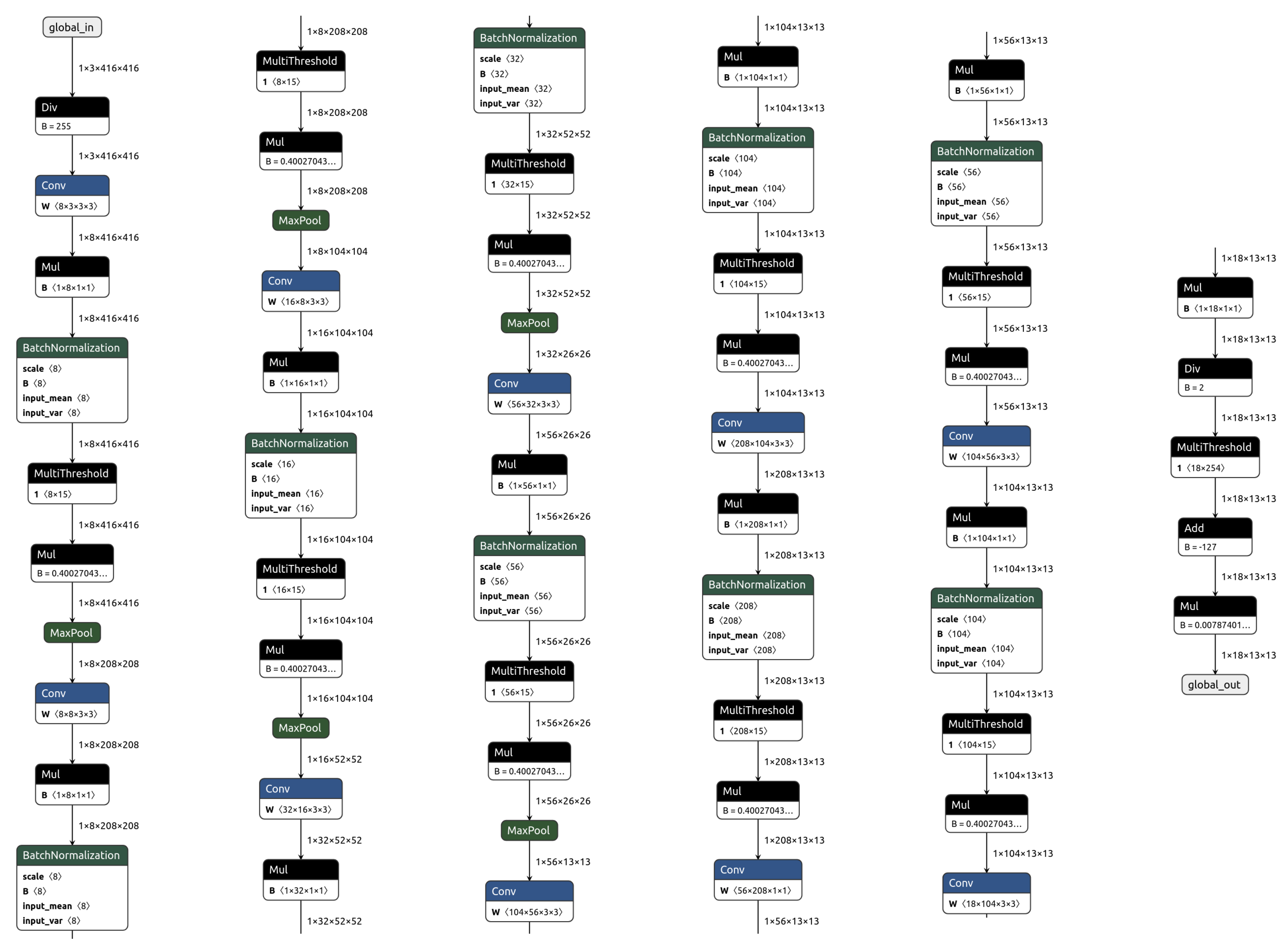
This command generates an .onnx file that encapsulates the quantized network architecture and learned parameters, ready for subsequent synthesis and deployment on FPGA hardware. A visual representation of this model, obtained using the ONNX visualization tool Netron [67], can be seen in Figure 3.

3.3. Coral AI Board Export

In order to effectively compare the inference results and performance later obtained with this work against a Coral TPU device, another training run was performed, this time with full FP32 precision. Then, a tflite model was exported with int8 PTQ precision. This tflite model was then compiled by the edgetpu compiler to be used for inference on the Coral TPU. In order to perform the export, a newer, community-maintained, version of the libedgetpu module is required [68].

3.4. FINN Transformations: From ONNX to Synthesizable IP

The FINN build flow transforms an ONNX neural network model into synthesizable hardware IP cores. To do so, a sequence of steps are performed, as detailed in the following.

3.4.1. Transformation of ONNX Representation into a FINN Model Representation

The exported network already shown in Figure 3 contains Quant layers fed into MaxPool or Conv layers. The first transformation to be applied is morphing the graph into a usable FINN representation. This is achieved by invoking the ConvertQONNXtoFINN transformation, which consolidates the Quant nodes into MaxPool and Conv layers and transforms ReLUs (or other activations) into MultiThreshold nodes. Additionally, other transformations were applied to tidy up the network. For an in-depth explanation of these tidy-ups, the FINN source code can be consulted. However, for completeness, these transformations store information about tensor shapes and data types into the FINN-ONNX graph, as well as assigning each node a unique name that can later be used for layer specialization and folding.
Afterward, the inputs (INT8 tensors representing images) must be normalized to values between 0 and 1, as the network was trained on normalized images. This is accomplished by inserting a Div node before the first convolution. Figure 4 displays the results of these transformations.

3.4.2. Streamlining

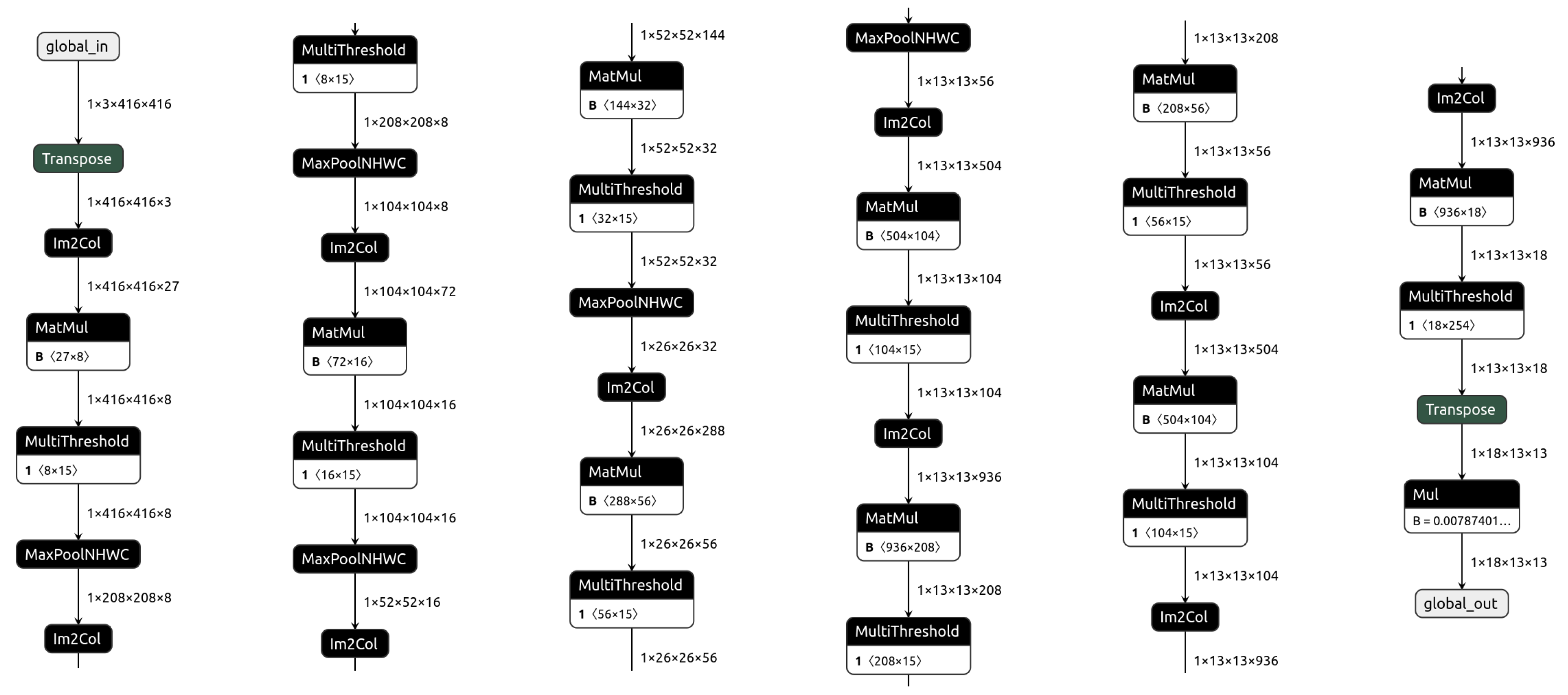
The next step is to streamline the network. This is necessary to eliminate floating-point operations, which are consolidated and then converted into MultiThreshold nodes. Moreover, convolutions need to be transformed—or lowered—into Im2Col and MatMul operations. The result of this operation is shown in Figure 5: all Conv nodes were replaced by Im2Col and MatMul nodes.

3.4.3. Hardware Mapping Transformation

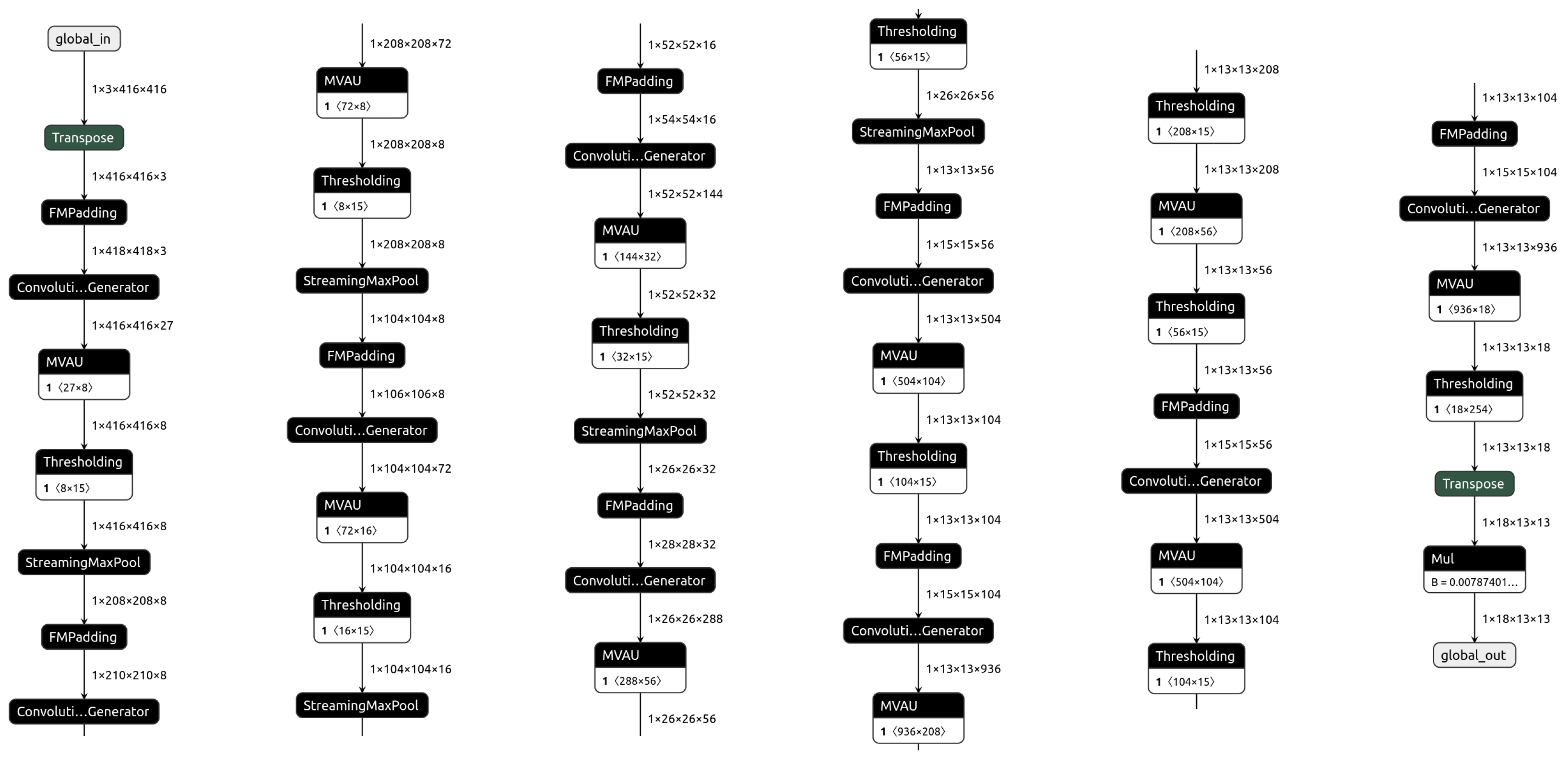
The subsequent transformations facilitate the effective mapping of all compatible layers to hardware-implemented functions. Specifically, all MatMul nodes were converted into FINN’s MVU, and the Im2Col nodes became FINN’s SWGs. Figure 6 illustrates the resulting network: as observed, two transposes remain. These are non-convertible layers resulting from the different data representations between YOLO and FINN. YOLO utilizes the NCWH representation, whereas FINN employs NWHC, where N is the batch number, W is the width, H is the height, and C is the channels of an image. This reordering of data can easily be dealt with in the driver that prepares the frames to be sent to the FPGA for inference.

3.4.4. Dataflow Partition

To proceed, it is necessary to prune the graph of incompatible nodes. This is accomplished by the CreateDataflowPartition transformation, which separates and merges into a subgraph all the synthesizable blocks. It is crucial that this operation does not produce more than one partition since, in the current development state, FINN is incapable of mapping multiple partitions onto the PL. In this case, Figure 7 shows that the operational block left behind is only a final Mul, which effectively is just a scaling operation that is to be performed on the PS instead to de-quantize the results.

3.5. Layer Specialization: RTL vs. HLS Implementations

FINN provides flexibility in how each neural network layer is implemented in hardware, allowing designers to choose between RTL and HLS implementations based on performance and resource utilization considerations. This section focuses on the specialization of the MVUs and the SWG—also known as CIG—units.
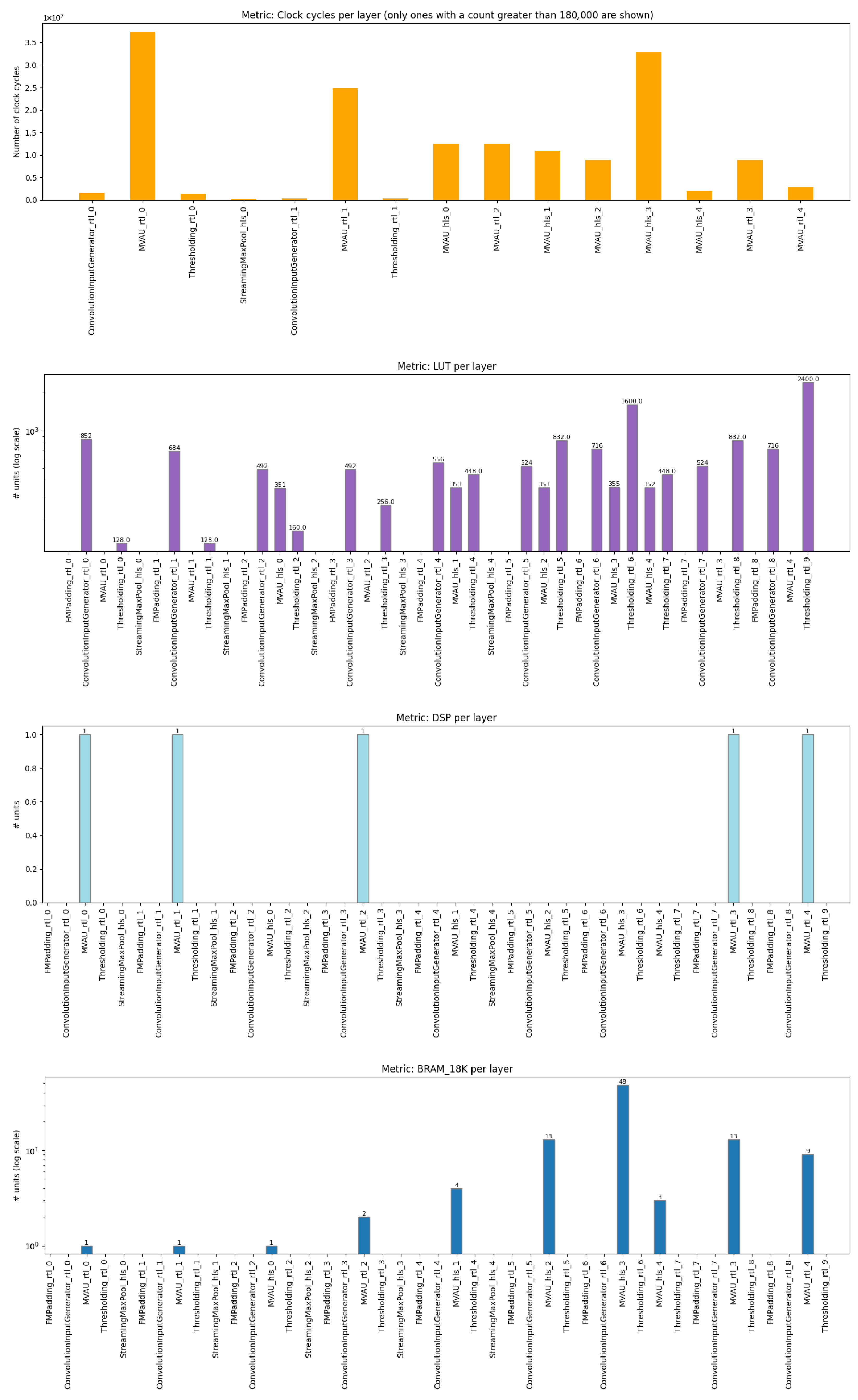
The transformation responsible for this specialization is called SpecializeLayers and requires an FPGA part to tailor the layers accordingly. If no manual configuration is provided, the transformation will always select the RTL variant of a component, reverting to an HLS implementation if no RTL code is available. To apply an external JSON configuration, the transformation ApplyConfig can be utilized. Figure 8 presents all the metrics for the default, fully folded, default-specialized layers, and Figure 9 depicts the fully specialized network.

3.5.1. Matrix-Vector Unit (MVU) Implementations

The MVU can be implemented using either RTL or HLS.

3.5.2. RTL Implementation

The RTL implementation of the MVU leverages Xilinx DSP slices. Recently, DSP packing was introduced in FINN [69]. This technique allows for multiple operations to be executed within a single DSP cycle, significantly enhancing throughput or, alternatively, reducing hardware utilization.
Table 4 outlines the available packing options, depending on the type of DSP slice used and the data types of the weights and activations. The Z-Turn Board is equipped with 220 DSP48E1 slices, and the trained YOLO network utilizes 4 bits for both the activations and weights in the internal layers, and 8-bit weights with 4-bit activations in the first and last convolutions. This configuration allows for efficient 2-fold or 4-fold packing of operations within an MVU. However, the RTL version currently does not support any LUT-style implementation.

3.5.3. HLS Implementation

The HLS implementation of the MVU supports both the DSP and LUT implementation styles but does not utilize them efficiently—particularly DSPs, as no packing is performed. For this reason, this implementation is discouraged since it will consume more resources to create a functional MVU unit. Nonetheless, there could be scenarios where this variant is beneficial: during the process of fully maximizing performance, if no further unfolding is possible due to DSP over-utilization, exploiting the abundant LUTs via this method proved to be a key factor.

3.5.4. Parallel Window Mode in SWG

The SWG can be implemented in both HLS and RTL variants. However, the RTL implementation features a parallel window capability [70], where multiple sliding windows—one for each channel—are processed simultaneously. This parallelism reduces the number of clock cycles required for convolution operations at the expense of necessitating a full SIMD unfolding.

3.6. Folding Strategies

This section discusses the folding strategies employed to achieve the best possible on-device performance.

3.6.1. Maximizing Performance Within Resource Constraints

Initially, the network is fully folded (i.e., every SIMD and PE attribute is set to 1). By applying a custom folding configuration—provided as a JSON file—to the ApplyConfig transformation, a specific folding can be tailored to each layer.
In this work, an iterative adjustment procedure was followed, each time unfolding the slowest layer and attempting to balance the cycle-per-layer metric while maintaining the network’s size within reasonable resource limits. Smaller layers (typically MaxPooling, SWG, and MultiThreshold units at the end of the network where feature maps are smaller) are kept fully folded to avoid wasting resources. The rationale is that there is no advantage in accelerating an already fast layer, as the network, when operating as a fully pipelined system (i.e., with a continuous stream of images being fed into it), is limited by the slowest layer.
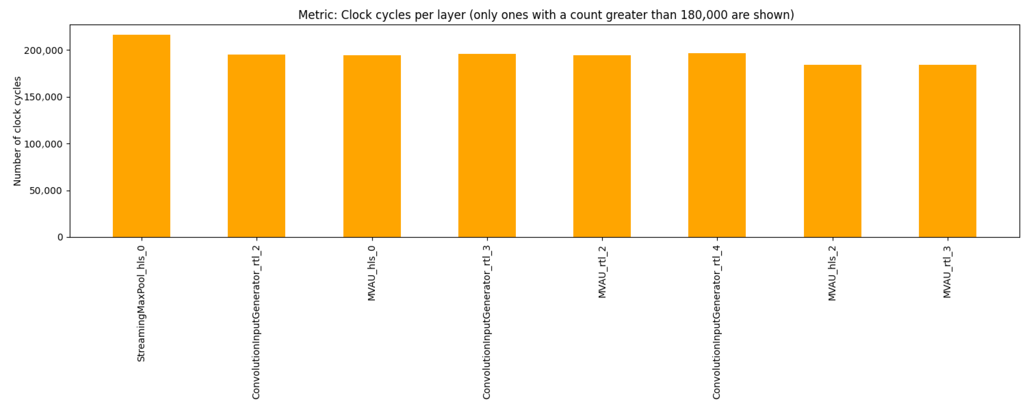
Iterations were performed until a bottleneck—i.e., the slowest layer being fully unfolded—was encountered. Figure 10 illustrates how the largest layers are flattened in relation to the slowest layer, StreamingMaxPool_hls_0.

3.6.2. Equalizing Resource Allocation Across Layers

After determining the optimal folding structure, with all layers being default-specialized, a utilization analysis was conducted. FINN allows for the estimation of resource usage with its analysis module. However, for some metrics, such as LUT, this is merely an estimation since Vivado optimizes and reallocates resources to find the best fit.
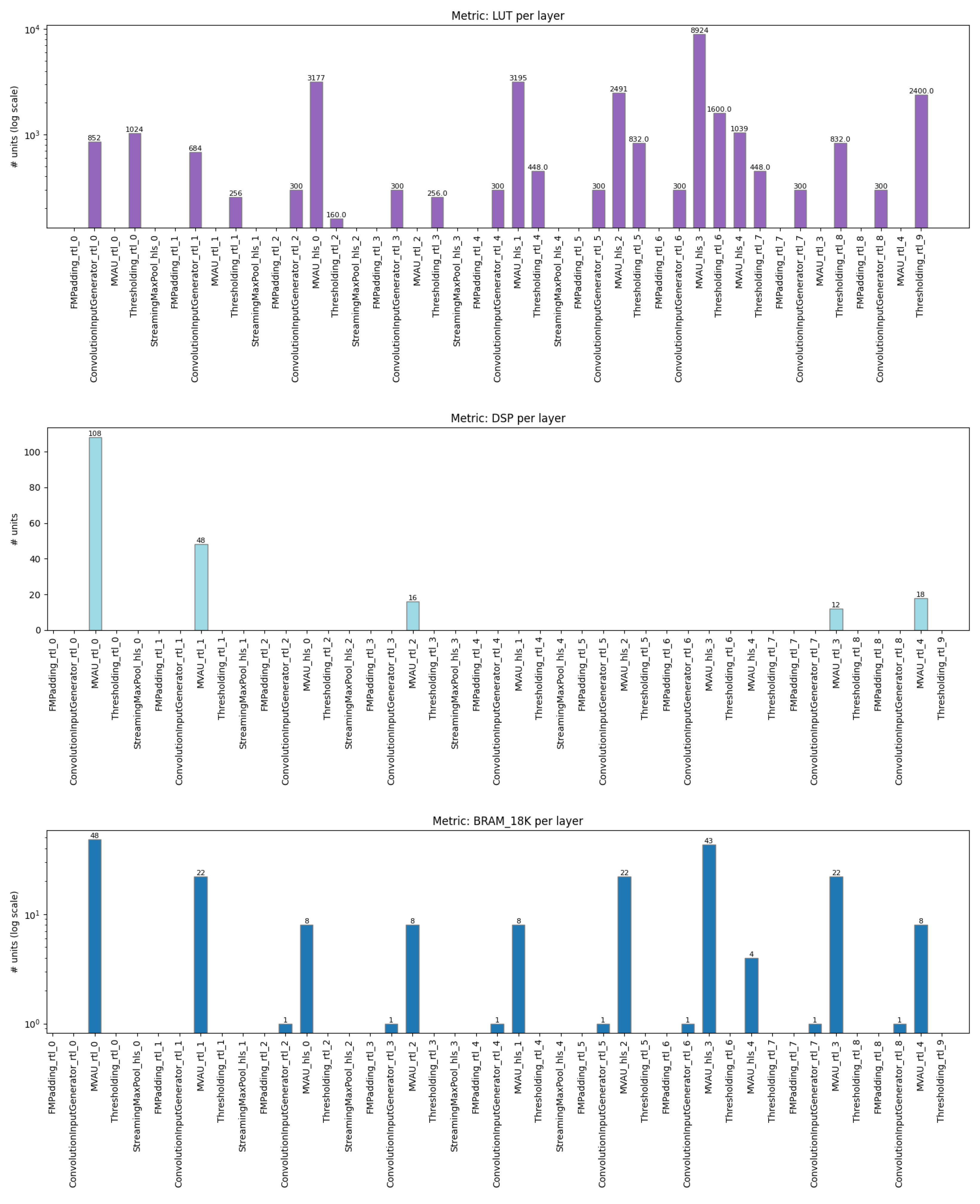
The most resource-intensive elements of the network are undeniably the MVU. Here, the HLS LUT implementation style was leveraged to maximize unfolding on these elements while avoiding DSP over-utilization, given the limited DSP capacity of the FPGA. A custom script to facilitate agile switching between specialization styles was developed using Python version 3.10.
The optimal configuration resulted in the outcome depicted in Figure 11.

3.7. FIFO Integration and Data Buffering

In a pipelined FPGA architecture, different layers may operate at varying clock cycle counts due to differences in computational complexity. FIFOs (First-In-First-Out buffers) are essential for buffering data between layers, ensuring smooth data flow and accommodating discrepancies in processing speeds while avoiding unwanted stalls that can severely impact overall network performance.

3.7.1. Implementation Challenges

Integrating FIFOs with appropriate lengths requires meticulous synchronization between layers. The process is time-consuming as it necessitates extensive simulation to experiment with various FIFO depths that minimize the stalling time of the various layers. Specifically, pyverilator and RTL simulation is employed to simulate and verify FIFO behavior under various operational scenarios.
Determining correct FIFO lengths is crucial: excessively short FIFOs result in a high percentage of layer stalling, while overly long FIFOs unnecessarily waste resources [71].

3.7.2. Initial FIFO Search Failure and StreamingMaxPool Issue

During the initial attempts to integrate FIFOs, a failure occurred due to the miscalculation of the maximum clock cycles required for certain operations. This led to the discovery of a deeper issue with the StreamingMaxPool HLS implementation. The HLS toolchain (Vitis) was found to require approximately 570,000 cycles—around 2.6 times more clock cycles than originally predicted for the StreamingMaxPool module, which was estimated at 216,320 cycles. This discrepancy prompted a thorough investigation of the HLS code. On paper, the HLS implementation of the operation should require the predicted number of cycles. However, it appears that Vitis implementations on large feature maps fail to optimize loop unrollings, causing an exponential increase in operation length. This issue could be mitigated by implementing a finely tuned RTL version, but it was beyond the scope of this work.
Final full hardware layer configurations, including all optimized FIFO depths, can be found in the repository [62] and are not included in this document due to their length.

3.8. Weight Storage Optimization

To maximize performance, all neural network weights were stored on-device within BRAM (Block RAM). This approach ensures rapid access to weights during inference, significantly reducing latency compared to when accessing weights from external RAM. Although accessing weights from external RAM is feasible, it would result in slower data retrieval rates via DMA and increased power consumption, which are detrimental to real-time inference applications.
FINN allows for a decision to be made, during the folding stage, regarding whether to use internal or external weights.

3.9. Vitis HLS Code Generation

After crafting the optimized network, it is time to commence the build process. The first step involves exporting all RTL code to the build directory. This is accomplished via PrepareIP transformation.
Next, all HLS code must be converted into RTL code via Vitis HLS Synthesis. This step is performed by the HLSSynthIP transformation and can be time-consuming.

3.10. IP Stitching and Vivado Synthesis

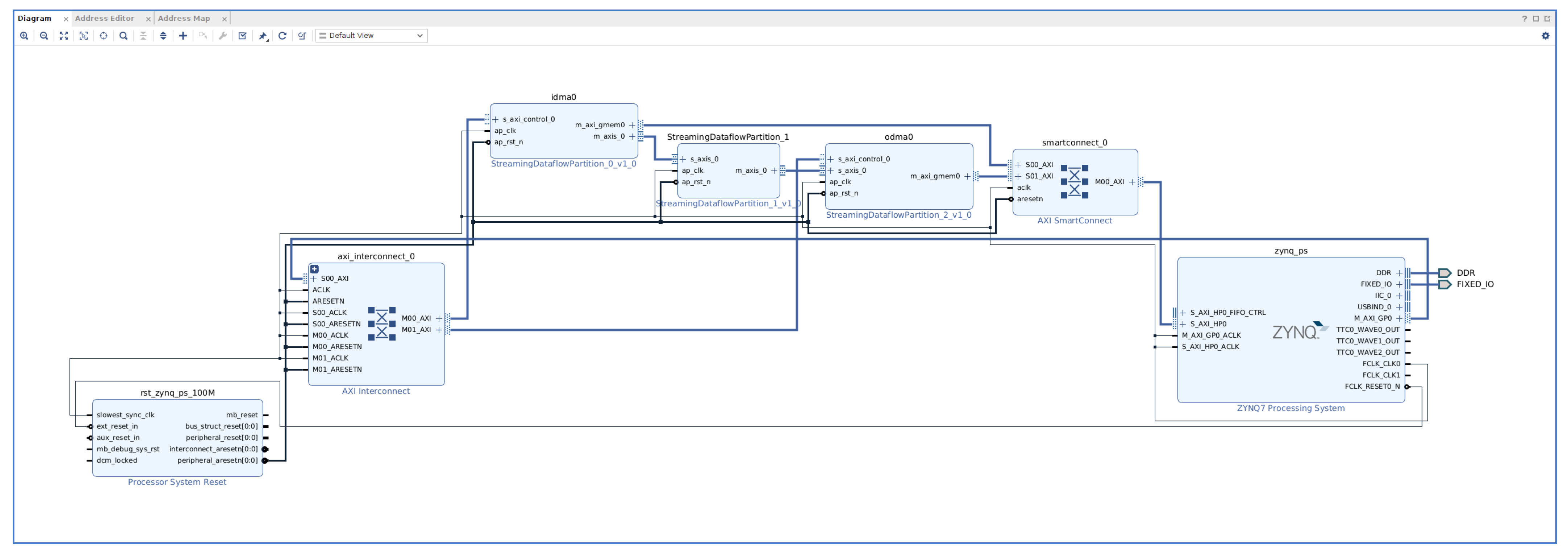
Once all individual IP cores have been generated and optimized, the next step involves stitching these IP cores together into a cohesive hardware design. This step is executed by the CreateStitchedIP transformation and is only required if the network needs to be exported or integrated into a larger design. Figure 12 illustrates the stitched FINN project.
Alongside the main StreamingDataflow_Partition module, two additional idma and odma modules are created. These serve as intermediaries to communicate with the DRAM, fetching input frames and outputting inference results, respectively.

3.10.1. Vivado Synthesis and Implementation

With the IP cores interconnected, Vivado is employed to synthesize and implement the design via the ZynqBuild transformation. This is the most time-consuming transformation as it involves the synthesis and place-and-route of the entire network. Figure 13 displays the physical mapping of the components onto the FPGA fabric.

3.10.2. PYNQ Driver Integration

The PYNQ driver is a Python module that simplifies communication with the newly created IP cores on the PL side. It automates the folding, packing, and transmission of frames to the DMA for inference operations. The auto-generated package includes the following:
  • A Python class that interfaces with the IP cores via MMIO.
  • Functions to handle data packing and communication with the DMA.
  • A class to upload the generated bitfile onto the FPGA, specifying the target clock frequency (adjustable at runtime) and the batch size of frames to be sent to the DMA.

3.11. Streaming Driver for TPU-like Implementations

The automatically generated PYNQ driver is a very low-level abstraction on the HW accelerator. The seamless integration of the FPGA-based neural network accelerator with external devices can be pivotal for real-time image and video recognition applications. To facilitate this integration, a Python-based driver and communication server were developed, enabling efficient data exchange and control over Ethernet. This section elucidates the development approach, underlying architecture, and the rationale behind key implementation decisions. It encompasses the design of a coherent pipeline, leveraging multithreading, the establishment of a robust packet exchange system, the processing workflow, and the dynamic configuration of the FPGA board using a custom model format (.fnn).
The code for both the client and server sides is provided in the repository [62].
The developed system comprises two primary components: the InferServer running on the FPGA board and the InferClient residing on the client device. Communication between these components is facilitated via WebSockets over Ethernet, enabling bidirectional data transfer and control commands. The server handles model loading, inference requests, and status reporting, while the client manages video capture, preprocessing, inference request dispatching, and result visualization.
Figure 14 shows a block diagram of the architecture.

3.11.1. Development Approach

The development of the driver and communication server was guided by the necessity for a responsive, scalable, and maintainable system. The approach encompassed designing a modular pipeline that efficiently handles data flow and processing tasks, implementing a reliable communication protocol, and ensuring dynamic configurability of the FPGA board, rendering the device similar to a TPU that can be loaded with a predefined model and can be used to execute accelerated inference only, while maintaining the other phases on another, more optimized processing element.

3.11.2. Pipeline Architecture and Multithreading

To achieve a coherent and efficient data processing pipeline, multithreading was employed on the client side to parallelize distinct stages of the workflow. The pipeline consists of the following key threads:
  • Capture Thread: Responsible for capturing video frames from a specified source (e.g., webcam or video file) using OpenCV. Captured frames are preprocessed and enqueued for inference.
  • Frame Dispatcher Thread: Retrieves preprocessed frames from the capture queue, formats them into binary messages with appropriate headers, and dispatches them to the InferServer via WebSockets.
  • Post-processing Thread: Collects inference results from the inference result queue, matches them with the original frames, and performs necessary post-processing tasks such as bounding box rendering.
  • Display Thread: Renders the post-processed frames to the user interface, enabling the real-time visualization of inference results.
This multithreaded architecture ensures that each stage operates concurrently, thereby maximizing throughput and minimizing latency. The use of thread-safe queues facilitates synchronized data exchange between threads, preventing bottlenecks and ensuring data integrity.

3.11.3. Communication Protocol

A robust communication protocol was established to handle both control commands and inference data. The protocol distinguishes between textual JSON messages and binary data packets:
  • JSON Messages: Utilized for control commands such as model loading (load_model) and status inquiries (status). These messages enable on-the-fly configuration and monitoring of the InferServer.
  • Binary Messages: Employed for transmitting inference requests and results. Binary messages consist of a custom header followed by payload data, facilitating efficient and compact data exchange.

3.11.4. JSON Command Handling

The InferServer interprets JSON messages to execute specific commands:
  • load_model: Initiates the loading of a new neural network model onto the FPGA board. The model is provided in a custom .fnn format, which includes all necessary information for configuration and deployment, such as the bitstream and the hardware definition file, a dictionary containing input and output shapes definitions and model metadata, such as name and version.
  • status: Retrieves the current status of the server, including model loading state, queue sizes, and active client connections.
These commands are parsed and routed to appropriate handlers within the server, ensuring an organized and maintainable code structure. Moreover, robust file integrity is employed making sure that the loaded model corresponds to the client’s target by using MD5 checksums.

3.11.5. Binary Inference Requests and Responses

Inference requests are sent as binary messages containing the following:
  • Header (16 bytes):
    frame_id (4 bytes, integer): Unique identifier for the frame.
    width (4 bytes, integer): Width of the frame.
    height (4 bytes, integer): Height of the frame.
    channels (2 bytes, short): Number of color channels.
    dtype_code (2 bytes, short): Data type code indicating the format of the payload.
  • Payload: Raw image data bytes.
Responses from the server follow a similar binary structure, containing the inference results corresponding to the submitted frames.

3.11.6. Inference Processing Workflow

The inference processing workflow is designed to handle high-throughput data while maintaining synchronization between capture, processing, and display stages.

3.11.7. Frame Capture and Preprocessing

The Capture Thread employs OpenCV to acquire frames from the designated source. Each frame undergoes preprocessing steps, including resizing and color channel inversion, to match the input requirements of the neural network model. The preprocessed frames are then enqueued for inference, ensuring that the inference pipeline receives data in a consistent and expected format.

3.11.8. Dispatching Inference Requests

The Sender Thread dequeues preprocessed frames and constructs binary messages adhering to the established communication protocol. Each message is assigned a unique frame_id to facilitate result matching. The messages are transmitted to the InferServer via an asynchronous WebSocket connection, enabling non-blocking and efficient data transfer.

3.11.9. Batch Processing on the Server

Upon receiving inference requests, the InferServer aggregates incoming frames into batches, optimizing the utilization of FPGA resources. The server employs a multithreaded inference worker that processes batches of up to 100 frames, executing the neural network model on the FPGA accelerator. This batching strategy balances performance and resource constraints, ensuring high throughput without overloading the system.

3.11.10. Post-Processing and Result Visualization

Inference results are received by the Post-Processing Thread, which correlates them with the original frames using the frame_id. Post-processing steps, such as bounding box detection and rendering and result annotation, are performed to allow the interpretability of the outputs. The processed frames are then forwarded to the Display Thread for real-time visualization, providing immediate feedback to the user.

3.11.11. Dynamic Board Configuration Using .fnn Format

A key feature of the developed system is the ability to dynamically configure the FPGA board by loading different neural network models without manual intervention. This is achieved through a custom .fnn file format, which encapsulates all necessary information for model deployment.

3.11.12. Structure of the .fnn File

The .fnn file is a zipped archive containing the following:
  • model.bit: The bitstream file for FPGA configuration.
  • model.hwh: The hardware handoff file detailing the FPGA’s hardware configuration.
  • model.pkl: A pickle file containing model shape dictionaries and other metadata.
  • model_info.json: A JSON file providing essential information such as maximum clock frequency, model name, and the dataset on which the model was trained.

3.11.13. Loading and Verifying the Model

Upon receiving a load_model command, the InferServer performs the following steps:
  • Model Extraction: Decodes the base64-encoded .fnn file and extracts its contents into a designated directory.
  • Integrity Verification: Checks for the presence of all required files (model.bit, model.hwh, model.pkl, model_info.json) to ensure the model archive is complete and uncorrupted.
  • Metadata Parsing: Loads and verifies the model_info.json file to extract configuration parameters such as clock frequency and model metadata.
  • FPGA Configuration: Utilizes the PYNQ driver to load the bitstream onto the FPGA, configuring the hardware accelerator with the new model.
  • Queue Initialization: Initializes the inference request queue and starts the inference worker thread to begin processing incoming data.

4. Results

4.1. Network Training Results

The YOLOv3-Tiny model, was chosen, although it is not the most accurate or newest model, due to its smaller footprint and ability to output acceptable inference results. Training was performed using a single class, encompassing cars objects only.
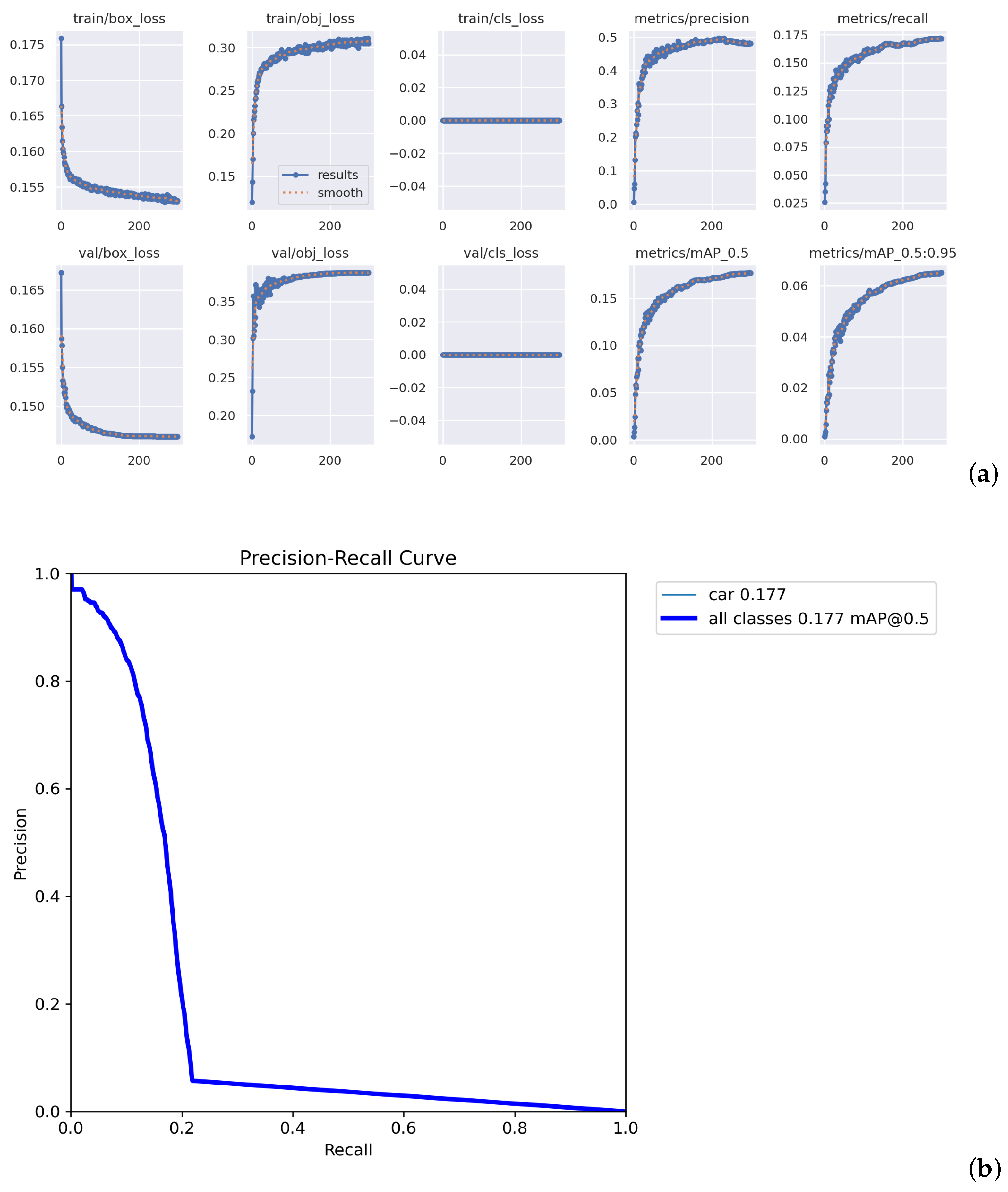
The results of the training run can be found in Figure 15. Although the results are not the brightest, for the scope of this work, the network’s accuracy is more than sufficient. Future works may try to improve the accuracy by further tweaking the model, or by running fine-tuning runs and adjusting the used hyperparameters.
Table 5 shows the final results of a 300-epochs training run performed on the VisDrone cars-only dataset. From the final epoch results, the single-class (“car”) precision ( P ) on the training set settled at around 48 % , while recall ( R ) remained near 17 % . This combination yielded an mAP of roughly 17.7 % at IoU = 0.5 . As a reference, the original YOLOv3-Tiny network trained on the same dataset achieved an mAP of nearly 42%. This reduction in accuracy was expected, since the pruned model uses only one detection branch, instead of the two in the original model. The two branches were intended to process features at different scales (dimensions), so removing one of them fundamentally halves the number of objects that could be detected, as demonstrated by the halved recall.
Such a modest detection accuracy, though not competitive by typical standards, fulfills the primary goal of this work, which emphasized optimizing resource usage and computational performance on an FPGA-based system, rather than maximizing predictive metrics. Consequently, while the mAP might appear low, the network still provides an illustrative benchmark for exploring quantization and high-throughput hardware inference. Moreover, if the intended usage is onboard a drone that can be flown at a standard altitude the scale of the objects to be recognized can be assumed to be essentially fixed. Indeed, empirical evidence on drone imagery acquired by us, as will be shown later in Section 4.5, demonstrated a much higher object identification rate (recall).

4.2. FPGA Implementation Results

4.2.1. Synthesis Reports

Synthesis reports offer detailed information on the following:
  • Resource utilization (LUT, DSP, BRAM usage), as shown in Figure 16.
  • Timing analysis, including setup and hold times, as illustrated in Figure 17.

4.2.2. RTL Simulation

RTL simulation, performed using tools like pyverilator, verifies the functional correctness of the hardware design. It ensures that data flows correctly through the IP cores and that FIFOs operate as intended under various scenarios. This confirmed the correct working of the implemented system.

4.2.3. MAC Operations

The hardware implementation described in the previous sections was synthesized, placed, and routed on a Xilinx Zynq-7020 device. Table 6 summarizes the MAC operations required by each MVU layer, along with the quantization formats for weights and activations. The final design thus operates with a mix of 8 b and 4 b data for both weights and activations, reaching an aggregate of over 113 million MAC in 4 b–4 b format and an additional 37 million MAC in 8 b–8 b, plus a smaller number of 2.8 million 4 b–8 b multiplications.

4.2.4. PL Resource Utilization

Table 7 shows the estimated versus real resource utilization. The final design consumed 138 of the 140 available BRAM_18K blocks (98.57% utilization), 204 DSP slices out of 220 (92.73%), and about 41k LUT out of the device’s 53.2k total LUT capacity (78.2%). The gap between estimates and measured utilization is explained by Vivado’s optimizations during logic synthesis and place-and-route. In particular, since the required BRAM_18K modules were acutally more than the available ones, some of them were converted in LUT as BRAM. Moreover Vitis HLS components, in particular, can sometimes produce logic that uses more LUT resources than a more refined RTL design might demand, especially when certain blocks fail to pack or fold as intended.

4.2.5. Performance Estimation, Simulation, and Evaluation

Table 8 compares the originally estimated throughput, drawn from the static analysis of cycles and a purely mathematical cycle budget, to the results obtained through an RTLSim functional simulation performed with Verilator [72] and the final real-world measurements at 100 MHz with a batch size of 100. The original estimate suggested more than 460 FPS was achievable, whereas the RTLSim-based simulation captured a noticeably lower 134 FPS. The final actual performance from the deployed system settled at around 104 FPS. There are several reasons for the discrepancy. First, the mathematical estimate overlooks certain overheads introduced by memory transactions, pipeline boundaries, and partial stalling among streaming layers. Next, even the RTLSim functional simulation does not fully capture the driver overhead and the real-world latencies present when interfacing with the PS side of the Zynq device. Indeed, replacing the auto-generated Python driver with custom-written bare-metal code allowed the full 134 FPS to be attained on the physical hardware. One specific layer (StreamingMaxPool_hls_0, see Section 3.7.2 for more details), implemented via Vitis HLS, proved notably suboptimal in practice, consuming far more clock cycles than the naive cycle-based analysis suggested. This bottleneck alone led to a substantial drop in the effective throughput by 3.43 times.
Finally it is worth noting that although the total predicted cycles are 4.5 million, which leads to a single-image latency of 45.87 ms, the real latency, with batch size 1, is measured to be only 11.56 ms.

4.2.6. Frequency Scaling Performance Variations

Frequency-scaling experiments were performed at three clock rates for the PL: 50, 100, and  200 MHz.
The measured throughput actually scales roughly linearly with clock frequency, as could be expected. At 50 MHz, the batch size = 1 inference took around 22.77 ms, yielding about 44 FPS, whereas raising the clock to 100 MHz improved the throughput to about 86 FPS. Doubling again to 200 MHz led to roughly 165 FPS. The throughput_test() results, visible in Table 9, were obtained by directly feeding random data directly via DRAM transfers, avoiding unnecessary data reshaping and repacking. The performance loss between the two batch sizes is about 17%, consistent with frequency scaling, with batch size = 100 achieving the best results: this difference is created by the streaming architecture and pipelined structure of the network. Sending 100 samples on the RAM, fills the whole pipeline and ensures the maximum performance, while when copying one frame at a time one must wait for the pipeline to be flushed, hence reducing the performance.
For the real data inference, the FINN Python driver was used, with a batch size of 1, to execute inference on a video stream. One must note that the overhead from the FINN-generated driver implies an additional baseline latency introduced in the “copy data to/from device” routines and the packing/unpacking stages. Consequently, as shown in Table 10, the measured end-to-end latencies achieve higher values than the purely hardware-limited ones.
The penalty introduced by the FINN standard driver reduces the actual FPS throughput by 21 % at 50 MHz, 35 % at 100 MHz, reaching a staggering 50 % at 200 MHz. This is expected, since the inference time scales with the frequency, while the total amount of time wasted in data repack and transformation remains fixed.

4.3. Power Consumption

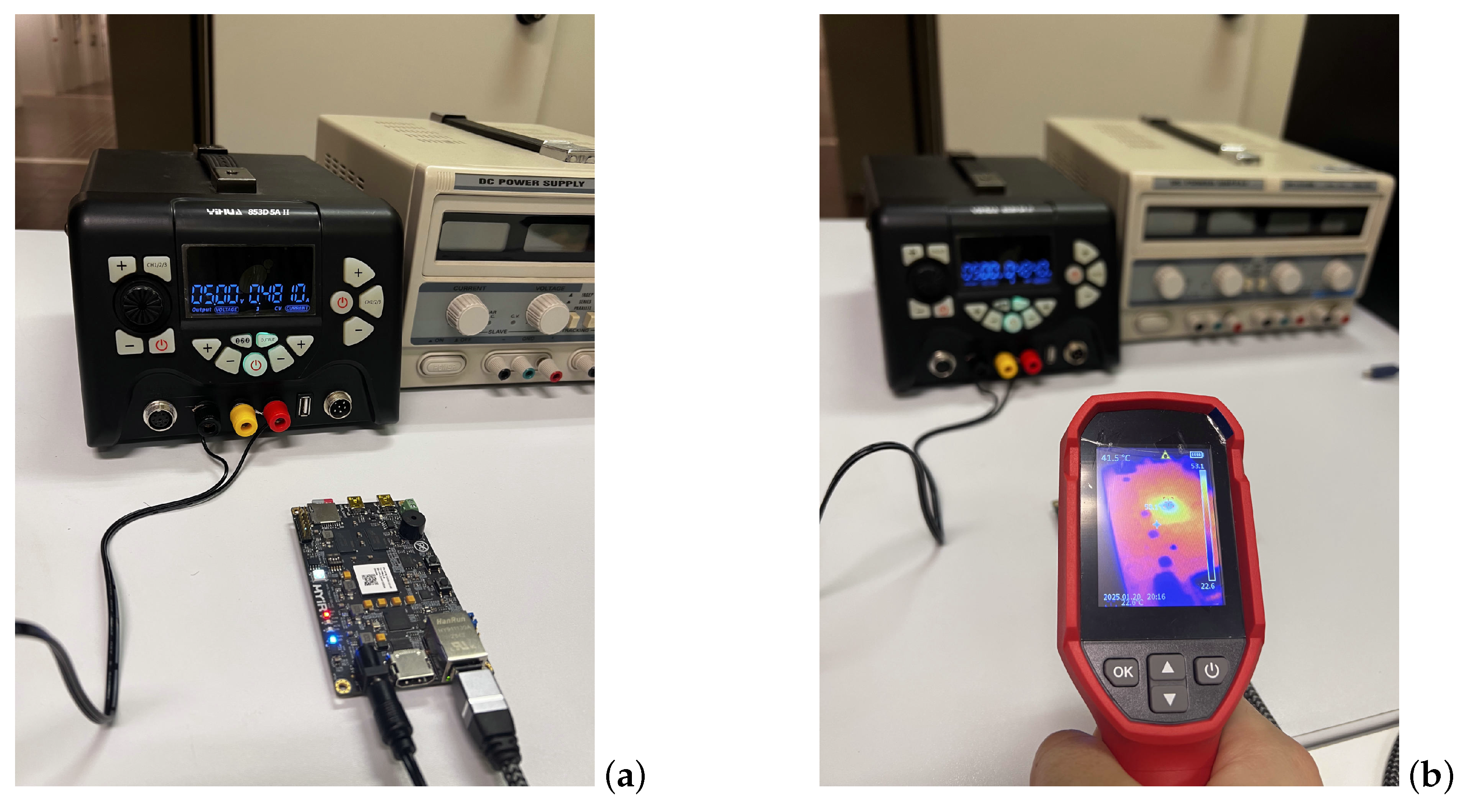
The power consumption estimation was performed by the Vivado power analysis tool. The real-world power analysis was performed by powering the entire board through a power bench, outputting 5 V DC, and measuring the current drawn, as shown in Figure 18. As can be seen, thermal shots were also taken using an IR thermal camera pointed at the SoC of the board.

4.3.1. Vivado Power Estimation

Table 11 reports the power estimates generated by Vivado for the top-level design and some key sub-blocks. These values represent the tool’s estimation of the dynamic power consumed by each module and offer a useful benchmark against which the measured consumption can be compared. Although the dynamic power for the programmable logic is estimated to be around 3.129 W in the Vivado report, the measured consumption is considerably lower. This difference is expected because the Vivado estimates are generated under worst-case or synthetic conditions and do not account for the optimizations that occur during the runtime.
Table 12 provides a more detailed breakdown of the on-chip power consumption according to different resource types.

4.3.2. Measured Power Consumption

Power consumption was measured at three frequency points under continuous inference load. The board idle consumption, with the bitstream not yet loaded, remained at around 1.9 W due to the PS and DRAM. At the inference time, with  50 MHz PL clock, total power increased to roughly 2.12 W, which increased to 2.38 W at 100 MHz and then to about 2.55 W at 200 MHz. Table 13 summarizes these measured values.
It is noteworthy that the idle power of about 1.9 W is almost entirely attributable to the PS and DDR memory, which indicates that the board’s firmware is not fully optimized for low-power operation, especially when not adjusting the PS ARM clock based on the load and always keeping it at the maximum frequency.
Taking into consideration that 1.9 W is drawn by the PS, the inference engine on the PL only draws between 0.22 W and 0.65 W (depending on clock frequency).
Table 14 shows some performance-per-watt metrics using the whole package power draw, because it is not possible to exclude the PS from a real-world context. As mentioned previously, implementing some power-saving functions on the Linux kernel that runs on the PS could greatly increase the FPS/W figure of merit, but this is beyond the scope of the present research.
Notably, the board performs much better at high frequency rates: this is again because of the static power consumption of the PS, which is more prominent with lower frequencies.
Finally, a temperature measure with an infrared thermal camera was taken for a comparison of Vivado’s maximum ambient estimated temperature, set at 46.3 °C, with the measured temperature, set at at 53.1 °C, on the die. No thermal dissipation apart from static air radiation was applied.

4.4. End-to-End System Throughput and Latency

The server-based architecture detailed in Section 3.11 was used for this test. The aim was to evaluate the performance of the developed architecture if used as an accelerator for external system. Despite every effort being made to pipeline every step of the process, separating them into various threads, the final throughput depended strongly on network latency and conditions. Moreover, the WebSocket performance was found to vary greatly between different operating system implementations and, of course, also depends on the network infrastructure.
However, through increasing the maximum internal queue size of WebSocket packets to a high value on the server side (FPGA), it was possible to obtain somewhat repeatable and consistent results. Specifically, the InferServer, running the PL at a 200 MHz clock frequency, took about 12 ms for each inference, as expected when using the standard FINN driver. The network delay was measured using both WiFi and wired Ethernet connections. On a system connected to the FPGA via WiFi, the maximum measured stream latency was around 130 ms, while with a direct Ethernet connection the maximum was about 10 times lower, at around 13 ms. With the wired connection, it was then possible to reach a 30 FPS throughput while directly streaming from a camera in real time using a macOS operating system for the client.
A throughput of 30 FPS represents a significant loss of performance compared to the capabilities of the inference engine, but it is still better than, e.g., the 18 FPS achieved in [63] when using a very similar setup (TCP/IP streaming to the same model of FPGA, using the same network architecture). This is likely due to many unnecessary data-move operations, copying and conversion between raw buffer arrays and the numpy array for each new frame received by the FPGA server, which are difficult to control with the current Python-based implementation that leverages the standard FINN driver. However, it is reasonable to expect that this overhead can be greatly reduced in future with the C implementation of the driver and communication interface.

4.5. Real-World Application Results

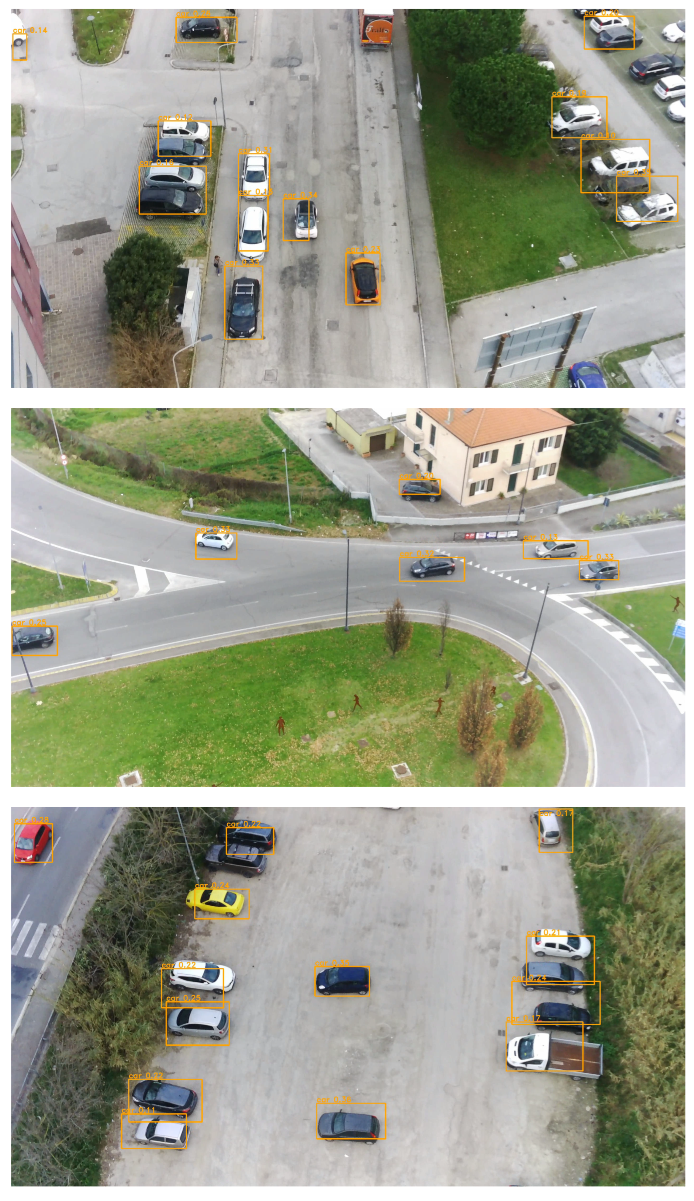
Finally, to assess the performance of the complete system on a realistic use case, we captured footage from a drone flown over roads and parking lots. The inference results from a few frames extracted from the video can be observed in Figure 19.
As can be seen, despite having a nominally low recall on the validation set, almost all of the cars were correctly detected and localized, demonstrating that the system can actually be used on the field.

5. Discussion

After showing the measurements of the performance obtained in this work, it can be useful to put these into perspective by comparing this work to some related works.

5.1. Comparison with Coral TPU

As a first step, let us explore the performance of competing HW implementations such as TPUs. Two distinct driver configurations were used: libedgetpu in standard mode and in max mode. Measured latencies with the standard driver averaged around 9.69 ms per image, whereas the max variant achieved 6.73 ms. These times correspond to roughly 103 FPS and 149 FPS, respectively. The Coral device’s manufacturer-documented power consumption may reach about 2.4 W at its maximum internal frequency (500 MHz), suggesting that at half-frequency (250 MHz) it would be closer to 1.2 W. Such numbers are estimates drawn from the datasheet rather than being directly measured in the present experiments. Table 15 compares these results with the Zynq-7020. The Coral TPU, although specialized, delivers a similar performance range in terms of throughput, but does so with a simpler driver stack. Finally, in the results, only the batch size = 1 performance was shown to allow for a fair comparison, at the cost of degraded performance for this work.

5.2. Comparison with Existing YOLOv3-Tiny FPGA Implementations

Table 16 summarizes selected data points from the existing literature, including the FINN-R paper [12], the SATAY paper [48] (using the fpgaConvNet toolflow [32]), and the LPYOLO paper [63] (which has the exact same network definition used in this work), alongside our own implementation. The table highlights the FPGA platform, the network footprint (weights or overall hardware resource usage), reported throughput or latency, and measured or estimated power consumption. Apart from the network from the FINN-R paper (a Tincy-YOLO), all the other networks are YOLOv3-Tiny, with a 416 × 416 input image size. mAP is not considered at this time, because the datasets that the networks were trained upon are different.
As Table 16 shows, the performances achieved in this work ranged from 7 to 24 times higher than those achieved by the other proposals. Moreover, the highest FPS score after ours was achieved when using a VCU118 MPSoC, which costs over €15,000 while the development board used in this work costs around €150. It should be noted, however, that the models used on SATAY have higher precision, using 8-bit weights and 16-bit activations, which render the network heavier. Nonetheless, the resources required for implementing such networks are extremely higher compared to this work or the one by the LPYOLO authors. Lastly, a direct comparison with LPYOLO, with has the exact same network configuration as this work, shows an increase by almost 10× in raw throughput performance (FPS) and a 7.3× increase in power efficiency (FPS/W). This was made possible through the careful selection of the folding parameters on the FINN framework, which were tuned to maximimize the parallel execution of the layers whenever possible (see Figure 10) and full usage of the DSP units within the FPGA in parallel with fabric-instantiated units.

6. Conclusions

This work presented the complete design and implementation of a real-time neural network accelerator on a low-cost FPGA platform. Unlike most studies that focus on high-end devices, our approach targeted the Xilinx Zynq-7020, demonstrating that even resource-constrained FPGAs can deliver competitive performance when paired with appropriate quantization and hardware-aware optimization. A full workflow was developed, including the preparation of the software environment, the training and quantization of a YOLOv3-Tiny model, the automatic conversion into hardware with FINN, and the integration of a custom driver, enabling the FPGA to act as a TPU for real-time inference.
Experimental evaluation showed that the accelerator achieved up to 208 frames per second at 200 MHz, with a power consumption of only 2.55 W, resulting in a favorable balance between throughput and energy efficiency. Compared with commercial ASIC-based solutions such as Google’s Coral Edge TPU, the proposed design delivered a comparable inference speed while maintaining a similar power budget and offering greater design flexibility. Furthermore, when benchmarked against FPGA-based works in the literature, our accelerator outperformed existing solutions by a factor of three to seven in FPS/W, confirming the viability of low-cost FPGAs as efficient inference engines for embedded AI.
Future work might investigate two aspects: The first involves further optimizing the driver that runs on the PS. Its current Python implementation, which requires a full Linux system running on the PS, is neither energy-efficient nor very fast. Preliminary tests using a bare-metal C driver showed promising results, with at least a 20% power saving w.r.t. the Linux kernel, even without implementing frequency scaling, and the possibility of operating DMA transfers fully in parallel with the inference This way the driver overhead would reduce to basically zero and the full theoretical fabric throughput can be restored. The second aspect involves scaling to larger models, optimizing memory utilization, and extending the approach to domains such as UAVs and IoT devices, where cost, energy efficiency, and autonomy remain critical.

Author Contributions

Conceptualization, R.C., L.F. and G.B.; methodology, R.C., L.F. and G.B.; software, R.C.; validation, R.C. and G.B.; investigation, R.C.; writing—original draft preparation, R.C., L.F. and G.B.; writing—review and editing, L.F. and G.B.; visualization, R.C.; supervision, L.F. and G.B.; project administration, L.F. and G.B. All authors have read and agreed to the published version of the manuscript.

Funding

This research received no external funding.

Institutional Review Board Statement

Not applicable.

Informed Consent Statement

Not applicable.

Data Availability Statement

The original contributions presented in this study are included in the article. Further inquiries can be directed to the corresponding author.

Conflicts of Interest

The authors declare no conflicts of interest.

Abbreviations

The following abbreviations are used in this manuscript:
AIArtificial Intelligence
AOIArea of Interest
ASICApplication-Specific Integrated Circuit
AXIAdvanced eXtensible Interface
BNBatch Normalization
BNNBinarized Neural Network
CIGConvolution Input Generator
CLBConfigurable Logic Block
CMOSComplementary Metal–Oxide-Semiconductor
CNNConvolutional Neural Network
COCOCommon Objects in Context
CUDACompute Unified Device Architecture
CPUCentral Processing Unit
DLDeep Learning
DMADirect Memory Access
DNNDeep Neural Network
DPUDeep-Learning Processing Unit
DSPDigital Signal Processing
FPGAField-Programmable Gate Array
FPSFrames per Second
GPUGraphics Processing Unit
HLSHigh-Level Synthesis
HTTPHyperText Transfer Protocol
IMUInertial Measurement Unit
IoUIntersection over Union
IoTInternet of Things
IPIntellectual Property
ISAInstruction Set Architecture
LUTLook Up Table
MACMultiply And Accumulate
mAPMean Average Precision
MMIOMemory Mapped I/O
MVUMatrix-Vector multiplication Unit
NMSNon-Maximum Suppression
NPUNeural Processing Units
NVDLANVIDIA Deep Learning Accelerator
ONNXOpen Neural Network Exchange
OOMOut Of Memory
PEProcessing Element
PLProgrammable Logic
PSProcessing System
PTQPost-Training Quantization
QATQuantization-Aware Training
QONNXQuantized Open Neural Network Exchange
RTLRegister Transfer Level
RTOSReal Time Operating System
SIMDSingle Instruction, Multiple Data
SoCSystem on a Chip
SWGSliding Window Generator
TCPTransmission Control Protocol
TNSTotal Negative Slack
TOPSTera Operations Per Second
TPUTensor Processing Unit
WNSWorst Negative Slack
XSAXilinx Support Archive
YOLOYou Only Look Once

References

  1. Krizhevsky, A.; Sutskever, I.; Hinton, G.E. ImageNet Classification with Deep Convolutional Neural Networks. In Proceedings of the Advances in Neural Information Processing Systems; Pereira, F., Burges, C., Bottou, L., Weinberger, K., Eds.; Curran Associates, Inc.: Red Hook, NY, USA, 2012; Volume 25. [Google Scholar]
  2. Chen, J.; Ran, X. Deep Learning With Edge Computing: A Review. Proc. IEEE 2019, 107, 1655–1674. [Google Scholar] [CrossRef]
  3. Lane, N.D.; Bhattacharya, S.; Mathur, A.; Georgiev, P.; Forlivesi, C.; Kawsar, F. Squeezing Deep Learning into Mobile and Embedded Devices. IEEE Pervasive Comput. 2017, 16, 82–88. [Google Scholar] [CrossRef]
  4. Jouppi, N.P.; Young, C.; Patil, N.; Patterson, D.; Agrawal, G.; Bajwa, R.; Bates, S.; Bhatia, S.; Boden, N.; Borchers, A.; et al. In-datacenter performance analysis of a tensor processing unit. In Proceedings of the 2017 ACM/IEEE 44th Annual International Symposium on Computer Architecture (ISCA), Toronto, ON, Canada, 24–28 June 2017; pp. 1–12. [Google Scholar] [CrossRef]
  5. Umuroglu, Y.; Fraser, N.J.; Gambardella, G.; Blott, M.; Leong, P.; Jahre, M.; Vissers, K. FINN: A Framework for Fast, Scalable Binarized Neural Network Inference. In Proceedings of the 2017 ACM/SIGDA International Symposium on Field-Programmable Gate Arrays, Monterey, CA, USA, 22–24 February 2017; pp. 65–74. [Google Scholar]
  6. Katkuri, A.V.R.; Madan, H.; Khatri, N.; Abdul-Qawy, A.S.H.; Patnaik, K.S. Autonomous UAV navigation using deep learning-based computer vision frameworks: A systematic literature review. Array 2024, 23, 100361. [Google Scholar] [CrossRef]
  7. Rejeb, A.; Abdollahi, A.; Rejeb, K.; Treiblmaier, H. Drones in agriculture: A review and bibliometric analysis. Comput. Electron. Agric. 2022, 198, 107017. [Google Scholar] [CrossRef]
  8. Han, S.; Liu, X.; Mao, H.; Pu, J.; Pedram, A.; Horowitz, M.A.; Dally, W.J. EIE: Efficient Inference Engine on Compressed Deep Neural Network. In Proceedings of the 2016 ACM/IEEE 43rd Annual International Symposium on Computer Architecture (ISCA), Seoul, Republic of Korea, 18–22 June 2016; pp. 243–254. [Google Scholar] [CrossRef]
  9. Lamberti, L.; Bellone, L.; Macan, L.; Natalizio, E.; Conti, F.; Palossi, D.; Benini, L. Distilling Tiny and Ultra-fast Deep Neural Networks for Autonomous Navigation on Nano-UAVs. IEEE Internet Things J. 2024, 11, 33269–33281. [Google Scholar] [CrossRef]
  10. Lamberti, L.; Niculescu, V.; Barciś, M.; Bellone, L.; Natalizio, E.; Benini, L.; Palossi, D. Tiny-PULP-Dronets: Squeezing Neural Networks for Faster and Lighter Inference on Multi-Tasking Autonomous Nano-Drones. In Proceedings of the 2022 IEEE 4th International Conference on Artificial Intelligence Circuits and Systems (AICAS), Incheon, Republic of Korea, 13–15 June 2022; pp. 287–290. [Google Scholar] [CrossRef]
  11. Redmon, J.; Farhadi, A. YOLOv3: An Incremental Improvement. arXiv 2018. [Google Scholar] [CrossRef]
  12. Blott, M.; Preußer, T.B.; Fraser, N.J.; Gambardella, G.; O’brien, K.; Umuroglu, Y.; Leeser, M.; Vissers, K. FINN-R: An end-to-end deep-learning framework for fast exploration of quantized neural networks. ACM Trans. Reconfigurable Technol. Syst. (TRETS) 2018, 11, 1–23. [Google Scholar] [CrossRef]
  13. Calì, R. Performance-Focused Implementation of Neural Networks for Real-Time Image and Video Recognition on Hybrid FPGA-CPU Architectures. Available online: https://tesi.univpm.it/handle/20.500.12075/20897 (accessed on 29 August 2025).
  14. Iandola, F.N.; Han, S.; Moskewicz, M.W.; Ashraf, K.; Dally, W.J.; Keutzer, K. SqueezeNet: AlexNet-level accuracy with 50x fewer parameters and <0.5 MB model size. arXiv 2016, arXiv:1602.07360. [Google Scholar]
  15. Howard, A.G.; Zhu, M.; Chen, B.; Kalenichenko, D.; Wang, W.; Weyand, T.; Andreetto, M.; Adam, H. MobileNets: Efficient Convolutional Neural Networks for Mobile Vision Aplications. arXiv 2017, arXiv:1704.04861. [Google Scholar]
  16. Zhang, X.; Zhou, X.; Lin, M.; Sun, J. ShuffleNet: An Extremely Efficient Convolutional Neural Network for Mobile Devices. In Proceedings of the 2018 IEEE/CVF Conference on Computer Vision and Pattern Recognition, Salt Lake City, UT, USA, 18–23 June 2018; pp. 6848–6856. [Google Scholar] [CrossRef]
  17. Ma, N.; Zhang, X.; Zheng, H.T.; Sun, J. ShuffleNet V2: Practical Guidelines for Efficient CNN Architecture Design. In Proceedings of the Computer Vision—ECCV 2018, Munich, Germany, 8–14 September 2018; Springer: Cham, Switzerland, 2018; pp. 122–138. [Google Scholar]
  18. Tan, M.; Le, Q.V. EfficientNet: Rethinking model scaling for convolutional neural networks. In Proceedings of the International Conference on Machine Learning (ICML), Long Beach, CA, USA, 9–15 June 2019; pp. 6105–6114. [Google Scholar]
  19. Han, S.; Mao, H.; Dally, W.J. Deep compression: Compressing deep neural networks with pruning, trained quantization and Huffman coding. In Proceedings of the International Conference on Learning Representations (ICLR), San Juan, Puerto Rico, 2–4 May 2016. [Google Scholar]
  20. Jacob, B.; Kligys, S.; Chen, B.; Zhu, M.; Tang, M.; Howard, A.; Adam, H.; Kalenichenko, D. Quantization and Training of Neural Networks for Efficient Integer-Arithmetic-Only Inference. In Proceedings of the 2018 IEEE/CVF Conference on Computer Vision and Pattern Recognition, Salt Lake City, UT, USA, 18–23 June 2018; pp. 2704–2713. [Google Scholar] [CrossRef]
  21. Courbariaux, M.; Hubara, I.; Soudry, D.; El-Yaniv, R.; Bengio, Y. Binarized Neural Networks: Training Deep Neural Networks with Weights and Activations Constrained to +1 or −1. arXiv 2016. [Google Scholar] [CrossRef]
  22. Rastegari, M.; Ordonez, V.; Redmon, J.; Farhadi, A. XNOR-Net: ImageNet Classification Using Binary Convolutional Neural Networks. In Proceedings of the Computer Vision—ECCV 2016, Amsterdam, The Netherlands, 8–16 October 2016; Springer: Cham, Switzerland; 2016; pp. 525–542. [Google Scholar]
  23. Zhou, S.; Wu, Y.; Ni, Z.; Zhou, X.; Wen, H.; Zou, Y. DoReFa-Net: Training low bitwidth convolutional neural networks with low bitwidth gradients. arXiv 2017, arXiv:1606.06160. [Google Scholar]
  24. Sze, V.; Chen, Y.H.; Yang, T.J.; Emer, J.S. Efficient Processing of Deep Neural Networks: A Tutorial and Survey. Proc. IEEE 2017, 105, 2295–2329. [Google Scholar] [CrossRef]
  25. NVIDIA. Jetson GPU Family, Enables Powerful Computational Capabilities for Embedded Solutions. Available online: https://www.nvidia.com/it-it/autonomous-machines/embedded-systems/ (accessed on 29 August 2025).
  26. STMicroelectronics. STM32N6: Our Very Own NPU in the Most Powerful STM32 to Inaugurate a New Era of Computing. Available online: https://blog.st.com/stm32n6/ (accessed on 29 August 2025).
  27. Google. Google’s Edge TPU family, Coral AI. Available online: https://coral.ai/ (accessed on 29 August 2025).
  28. Hailo. Hailo-8 M.2 AI Acceleration Module. Available online: https://hailo.ai/products/ai-accelerators/hailo-8-m2-ai-acceleration-module/ (accessed on 29 August 2025).
  29. Zhang, C.; Li, P.; Sun, G.; Guan, Y.; Xiao, B.; Cong, J. Optimizing FPGA-based accelerator design for deep convolutional neural networks. In Proceedings of the ACM/SIGDA International Symposium on Field-Programmable Gate Arrays (FPGA), Monterey, CA, USA, 22–24 February 2015; pp. 161–170. [Google Scholar]
  30. Qiu, J.; Wang, J.; Yao, S.; Guo, K.; Li, B.; Zhou, E.; Yu, J.; Tang, T.; Xu, N.; Song, S.; et al. Going deeper with embedded FPGA platform for convolutional neural networks. In Proceedings of the ACM/SIGDA International Symposium on Field-Programmable Gate Arrays (FPGA), Monterey, CA, USA, 21–23 February 2016; Association for Computing Machinery: New York, NY, USA, 2016; pp. 26–35. [Google Scholar] [CrossRef]
  31. Nurvitadhi, E.; Venkatesh, G.; Marr, J.; Huang, R.; Sim, J.; Esmaeilzadeh, H. Can FPGAs beat GPUs in accelerating deep neural networks? In Proceedings of the ACM/SIGDA International Symposium on Field-Programmable Gate Arrays (FPGA), Monterey, CA, USA, 22–24 February 2017; pp. 5–14. [Google Scholar] [CrossRef]
  32. Venieris, S.I.; Bouganis, C.S. fpgaConvNet: A Framework for Mapping Convolutional Neural Networks on FPGAs. In Proceedings of the 2016 IEEE 24th Annual International Symposium on Field-Programmable Custom Computing Machines (FCCM), Washington, DC, USA, 1–3 May 2016; pp. 40–47. [Google Scholar] [CrossRef]
  33. Venieris, S.I.; Bouganis, C.S. fpgaConvNet: A toolflow for mapping diverse convolutional neural networks on FPGAs. arXiv 2017, arXiv:1711.08740. [Google Scholar]
  34. Liu, Z.; Dou, Y.; Jiang, J.; Xu, J.; Li, S.; Zhou, Y.; Xu, Y. Throughput-Optimized FPGA Accelerator for Deep Convolutional Neural Networks. ACM Trans. Reconfigurable Technol. Syst. (TRETS) 2017, 10, 1–23. [Google Scholar] [CrossRef]
  35. Li, R. Dataflow & Tiling Strategies in Edge-AI FPGA Accelerators: A Comprehensive Literature Review. arXiv 2025. [Google Scholar] [CrossRef]
  36. Yan, F.; Koch, A.; Sinnen, O. A survey on FPGA-based accelerator for ML models. arXiv 2024. [Google Scholar] [CrossRef]
  37. Chen, H.; Hao, C. DGNN-Booster: A Generic FPGA Accelerator Framework For Dynamic Graph Neural Network Inference. In Proceedings of the 2023 IEEE 31st Annual International Symposium on Field-Programmable Custom Computing Machines (FCCM), Marina Del Rey, CA, USA, 8–11 May 2023; pp. 195–201. [Google Scholar] [CrossRef]
  38. Carpegna, A.; Savino, A.; Carlo, S.D. Spiker+: A Framework for the Generation of Efficient Spiking Neural Networks FPGA Accelerators for Inference at the Edge. IEEE Trans. Emerg. Top. Comput. 2025, 13, 784–798. [Google Scholar] [CrossRef]
  39. Nag, S.; Susskind, Z.; Arora, A.; Bacellar, A.T.L.; Dutra, D.L.C.; Miranda, I.D.S.; Kailas, K.; John, E.B.; Breternitz, M.; Lima, P.M.V.; et al. LogicNets vs. ULEEN: Comparing two novel high throughput edge ML inference techniques on FPGA. In Proceedings of the 2024 IEEE 67th International Midwest Symposium on Circuits and Systems (MWSCAS), Springfield, MA, USA, 11–14 August 2024; pp. 1206–1211. [Google Scholar] [CrossRef]
  40. Jiang, Y.; Vaicaitis, A.; Dooley, J.; Leeser, M. Efficient Neural Networks on the Edge with FPGAs by Optimizing an Adaptive Activation Function. Sensors 2024, 24, 1829. [Google Scholar] [CrossRef]
  41. Bosio, R.; Minnella, F.; Urso, T.; Casu, M.R.; Lavagno, L.; Lazarescu, M.T.; Pasini, P. NN2FPGA: Optimizing CNN Inference on FPGAs With Binary Integer Programming. IEEE Trans.-Comput.-Aided Des. Integr. Circuits Syst. 2024, 44, 1807–1818. [Google Scholar] [CrossRef]
  42. Xilinx. Xilinx DPU Datasheet. Available online: https://docs.amd.com/r/en-US/pg338-dpu (accessed on 29 August 2025).
  43. NVIDIA. NVIDIA Deep Learning Accelerator (NVDLA). Available online: https://nvdla.org/ (accessed on 29 August 2025).
  44. Xilinx. Vitis AI: Support for Zynq-7000 Devices. Available online: https://adaptivesupport.amd.com/s/article/76742?language=en_US (accessed on 29 August 2025).
  45. Cesarano, G. FPGA Implementation of a Deep Learning Inference Accelerator for Autonomous Vehicles. Master’s Thesis, Politecnico di Torino, Turin, Italy, 2018. [Google Scholar]
  46. Wang, L. ZYNQ-NVDLA. Available online: https://github.com/LeiWang1999/ZYNQ-NVDLA?tab=readme-ov-file (accessed on 29 August 2025).
  47. Marino, V. Hardware Acceleration of AdderNet via High-Level Synthesis for FPGA. Master’s Thesis, Politecnico di Torino, Turin, Italy, 2024. [Google Scholar]
  48. Montgomerie-Corcoran, A.; Toupas, P.; Yu, Z.; Bouganis, C.S. SATAY: A Streaming Architecture Toolflow for Accelerating YOLO Models on FPGA Devices. arXiv 2023. [Google Scholar] [CrossRef]
  49. Toupas, P.; Yu, Z.; Bouganis, C.S.; Tzovaras, D. SMOF: Streaming Modern CNNs on FPGAs with Smart Off-Chip Eviction. arXiv 2024. [Google Scholar] [CrossRef]
  50. Kadi, M.A.; Rudolph, P.; Gohringer, D.; Hubner, M. Dynamic and partial reconfiguration of Zynq 7000 under Linux. In Proceedings of the 2013 International Conference on Reconfigurable Computing and FPGAs (ReConFig), Cancun, Mexico, 9–11 December 2013; pp. 1–5, ISSN 2325-6532. [Google Scholar] [CrossRef]
  51. Ma, Y.; Xu, Q.; Song, Z. Resource-Efficient Optimization for FPGA-Based Convolution Accelerator. Electronics 2023, 12, 4333. [Google Scholar] [CrossRef]
  52. Pistellato, M.; Bergamasco, F.; Bigaglia, G.; Gasparetto, A.; Albarelli, A.; Boschetti, M.; Passerone, R. Quantization-Aware NN Layers with High-throughput FPGA Implementation for Edge AI. Sensors 2023, 23, 4667. [Google Scholar] [CrossRef]
  53. Fraga-Lamas, P.; Ramos, L.; Mondéjar-Guerra, V.; Fernández-Caramés, T.M. A Review on IoT Deep Learning UAV Systems for Autonomous Obstacle Detection and Collision Avoidance. Remote Sens. 2019, 11, 2144. [Google Scholar] [CrossRef]
  54. Lahmeri, M.A.; Kishk, M.A.; Alouini, M.S. Artificial Intelligence for UAV-Enabled Wireless Networks: A Survey. IEEE Open J. Commun. Soc. 2021, 2, 1015–1040. [Google Scholar] [CrossRef]
  55. Zhou, L.; Yin, H.; Zhao, H.; Wei, J.; Hu, D.; Leung, V.C. A Comprehensive Survey of Artificial Intelligence Applications in UAV-Enabled Wireless Networks. Digit. Commun. Netw. 2024. [Google Scholar] [CrossRef]
  56. Maqueda, A.I.; Loquercio, A.; Gallego, G.; García, N.; Scaramuzza, D. Event-based vision meets deep learning on steering prediction for self-driving cars. In Proceedings of the IEEE Conference on Computer Vision and Pattern Recognition, Salt Lake City, UT, USA, 18–23 June 2018; pp. 5419–5427. [Google Scholar]
  57. Deng, J.; Shi, Z.; Zhuo, C. Energy-Efficient Real-Time UAV Object Detection on Embedded Platforms. IEEE Trans. Comput.-Aided Des. Integr. Circuits Syst. 2020, 39, 3123–3127. [Google Scholar] [CrossRef]
  58. Chen, T.; Du, Z.; Sun, N.; Wang, J.; Wu, C.; Chen, Y.; Temam, O. DianNao: A small-footprint high-throughput accelerator for ubiquitous machine-learning. SIGARCH Comput. Archit. News 2014, 42, 269–284. [Google Scholar] [CrossRef]
  59. Choi, K.; Sobelman, G.E. An Efficient CNN Accelerator for Low-Cost Edge Systems. ACM Trans. Embed. Comput. Syst. 2022, 21, 1–20. [Google Scholar] [CrossRef]
  60. Wang, Y.; Liao, Y.; Yang, J.; Wang, H.; Zhao, Y.; Zhang, C.; Xiao, B.; Xu, F.; Gao, Y.; Xu, M.; et al. An FPGA-based online reconfigurable CNN edge computing device for object detection. Microelectron. J. 2023, 137, 105805. [Google Scholar] [CrossRef]
  61. Procaccini, M.; Sahebi, A.; Giorgi, R. A survey of graph convolutional networks (GCNs) in FPGA-based accelerators. J. Big Data 2024, 11, 163. [Google Scholar] [CrossRef]
  62. Calì, R. Thesis Code Repository. Available online: https://github.com/sn0wst0rm/FINN-VisDrone-YOLO (accessed on 29 August 2025).
  63. Günay, B.; Okcu, S.B.; Bilge, H.c. LPYOLO: Low Precision YOLO for Face Detection on FPGA. arXiv 2022. [Google Scholar] [CrossRef]
  64. OKCU, S.B. Low Precision(quantized) Yolov5, Modified Verision of Ultralytics YOLOv5 Repo, Implementing Quantization Modules for PyTorch Using Brevitas. 2024. Available online: https://github.com/sefaburakokcu/quantized-yolov5 (accessed on 29 August 2025).
  65. Zhu, P.; Wen, L.; Du, D.; Bian, X.; Fan, H.; Hu, Q.; Ling, H. Detection and tracking meet drones challenge. IEEE Trans. Pattern Anal. Mach. Intell. 2021, 44, 7380–7399. [Google Scholar] [CrossRef] [PubMed]
  66. Kaggle. Kaggle: Your Machine Learning and Data Science Community. Available online: https://www.kaggle.com/ (accessed on 29 August 2025).
  67. Roeder, L. Netron, Visualizer for Neural Network, Deep Learning and Machine Learning Models. Available online: https://netron.app/ (accessed on 29 August 2025).
  68. feranick. Edge TPU Runtime Library (Libedgetpu). 2025. Available online: https://github.com/feranick/libedgetpu (accessed on 29 August 2025).
  69. Mrahorovic, M. Multi-Packed DSPs for MVU/VVU Layers · Xilinx/Finn · Discussion #1021. Available online: https://github.com/Xilinx/finn/discussions/1021 (accessed on 29 August 2025).
  70. Labs, X.R. Convolution Input Generator—FINN Documentation. Available online: https://finn.readthedocs.io/en/latest/internals.html#rtl-convolutioninputgenerator (accessed on 29 August 2025).
  71. Borras, H. Questions About the FIFO Depth Between Layers · Xilinx/Finn · Discussion #383. Available online: https://github.com/Xilinx/finn/discussions/383#discussioncomment-1449610 (accessed on 29 August 2025).
  72. Veripool. Verilator Software. Available online: https://www.veripool.org/verilator/ (accessed on 29 August 2025).
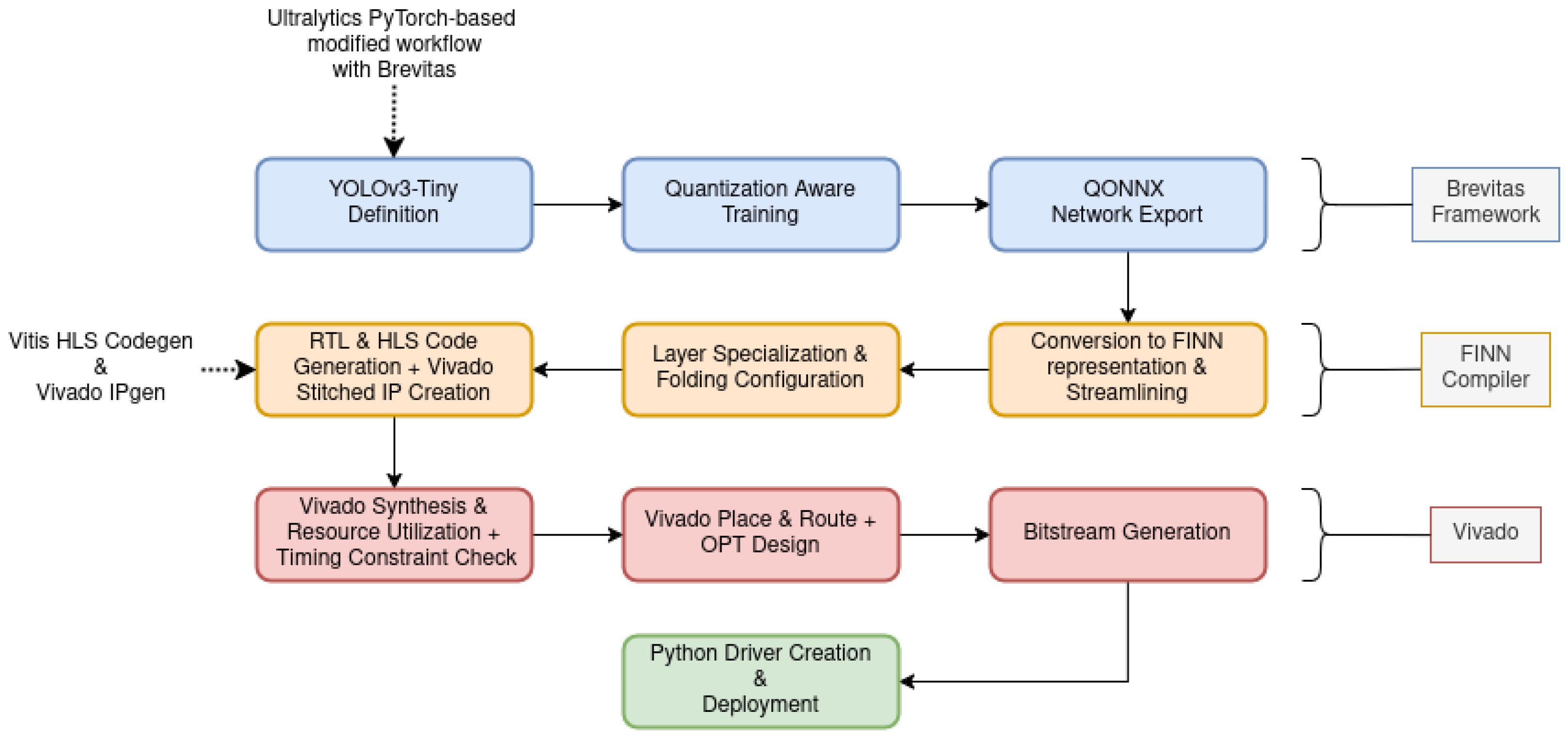
Figure 1. The design workflow that was followed to produce a working network in the FPGA.
Electronics 14 03993 g001
Figure 2. An aerial view of a street showing inference on the car class of the VisDrone dataset.
Electronics 14 03993 g002
Figure 3. Original quantized ONNX YOLOv3-Tiny network. The network was cut into three segments (from left to right) for visualization purposes.
Electronics 14 03993 g003
Figure 4. FINN-ONNX network. The network was cut into six segments (from left to right) for visualization purposes.
Electronics 14 03993 g004
Figure 5. The network after the streamline process. The network was cut into six segments (from left to right) for visualization purposes.
Electronics 14 03993 g005
Figure 6. The network is completely converted in hardware layers. The network was cut into six segments (from left to right) for visualization purposes.
Electronics 14 03993 g006
Figure 7. The Parent model, containing all the unsynthesizable layers and a StreamingDataflowPartition in-between. The PS will need to take care of the tasks outside the StreamingDataflowPartition, but they are trivial transpositions and scaling.
Electronics 14 03993 g007
Figure 8. Metrics for the fully folded and default-specialized network. Bars denote the number of specific resources required by each network layer.
Electronics 14 03993 g008
Figure 9. The layers are specialized into HLS or RTL variants. The network was cut into six segments (from left to right) for visualization purposes.
Electronics 14 03993 g009
Figure 10. The optimal Flat cycles-per-layer graph achieved.
Electronics 14 03993 g010
Figure 11. Utilization metrics for the optimal folding configuration. Bars denote the number of specific resources required by each network layer.
Electronics 14 03993 g011
Figure 12. The final stitched IP Vivado project.
Electronics 14 03993 g012
Figure 13. Visual Representation of the FPGA physical slices utilized.
Electronics 14 03993 g013
Figure 14. System architecture overview.
Electronics 14 03993 g014
Figure 15. Training results: (a) training result curves; (b) P R curve of the training results.
Electronics 14 03993 g015
Figure 16. Resource utilization report generated by Vivado.
Electronics 14 03993 g016
Figure 17. Timing analysis generated by Vivado.
Electronics 14 03993 g017
Figure 18. Bench setup for measuring both power an thermal properties of the board under load. (a) power bench–board setup; (b) thermal measurement setup.
Electronics 14 03993 g018
Figure 19. Shots taken with a drone to assess the on-field capabilities of the implemented network.
Electronics 14 03993 g019
Table 1. Architectural details of the quantized YOLOv3-Tiny Model.
Layer TypeInputOutputKernelStrideActivation
QuantConv416 × 416 × 3416 × 416 × 83 × 31QuantReLU
MaxPooling416 × 416 × 8208 × 208 × 82 × 22-
QuantConv208 × 208 × 8208 × 208 × 83 × 31QuantReLU
MaxPooling208 × 208 × 8104 × 104 × 82 × 22-
QuantConv104 × 104 × 8104 × 104 × 163 × 31QuantReLU
MaxPooling104 × 104 × 1652 × 52 × 162 × 22-
QuantConv52 × 52 × 1652 × 52 × 323 × 31QuantReLU
MaxPooling52 × 52 × 3226 × 26 × 322 × 22-
QuantConv26 × 26 × 3226 × 26 × 563 × 31QuantReLU
MaxPooling26 × 26 × 5613 × 13 × 562 × 22-
QuantConv13 × 13 × 5613 × 13 × 1043 × 31QuantReLU
MaxPooling13 × 13 × 10413 × 13 × 1042 × 22-
QuantConv13 × 13 × 10413 × 13 × 2083 × 31QuantReLU
QuantConv13 × 13 × 20813 × 13 × 561 × 11QuantReLU
QuantConv13 × 13 × 5613 × 13 × 1043 × 31QuantReLU
QuantConv13 × 13 × 10413 × 13 × 183 × 31QuantHardTanh
Table 2. Package versions used in the Kaggle environment.
PackageVersion
matplotlib3.5.1
numpy1.26.3
opencv-python4.10.0.84
pillow11.1.0
PyYAML6.0.2
requests2.32.3
scipy1.15.0
torch1.13.1
torchvision0.14.1
tqdm4.67.1
brevitas0.9.0
tensorboard2.15.2
pandas2.2.3
seaborn0.13.2
thop0.1.1.post2209072238
Table 3. Training configuration parameters.
ParameterValue
Number of Epochs300
Batch Size64
Image Size 416 × 416
OptimizerSGD
Patience30
Table 4. DSP Utilization for Different Configurations.
DSP TYPEActivations: [4,4]-bit (U)INT
Weights: [4,4]-bit INT
Activations: (4,8]-bit (U)INT
Weights: (4,8]-bit INT
HLS DSP1 MAC/DSP1 MAC/DSP
RTL DSP48E14 MAC/DSP2 MAC/DSP
RTL DSP48E24 MAC/DSP2 MAC/DSP
RTL DSP583 MAC/DSP3 MAC/DSP
Table 5. Validation results for the original and final pruned model, trained on the VisDrone dataset limited to the single class “car”.
MetricYOLOv3-Tiny
Original
YOLOv3-Tiny
Pruned
Precision (P)67.06%48.16%
Recall (R)38.44%17.16%
mAP@0.541.76%17.68%
Box loss0.12200.1531
Object loss0.16530.3049
Classification loss00
Table 6. Per-MVU MAC operations and weight parameters.
LayerMAC OperationsWeightsData Type
MVAU_rtl_037,380,0962168b–8b
MVAU_rtl_124,920,0645764b–4b
MVAU_hls_012,460,03211524b–4b
MVAU_rtl_212,460,03246084b–4b
MVAU_hls_110,902,52816,1284b–4b
MVAU_hls_28,858,30452,4164b–4b
MVAU_hls_332,902,272194,6884b–4b
MVAU_hls_41,968,51211,6484b–4b
MVAU_rtl_38,858,30452,4164b–4b
MVAU_rtl_42,847,31216,8484b–8b
Total(8 b–8 b)37,380,096(8 b)17,064
(4 b–4 b)113,330,048(4 b)333,632
(4 b–8 b)2,847,312
Table 7. Resource utilization: estimated vs. actual.
ResourceEstimatedActualAvailableUtil%
BRAM_18K20013814098.57
LUT26,69441,60553,20078.20
DSP20220422092.73
URAM0
Table 8. Estimated, simulated, and measured performance at 100 MHz.
MetricEstimatedRTLSimActual (FINN)
Total Cycles4,586,895 → critical path
Max Cycles (Node)216,320 (StreamingMaxPool_hls_0)741,670
Latency (ms)45.877.4111.56
Throughput (FPS)462.28134.83104.39
Table 9. Throughput Test Results at Different PL Clock Frequencies.
Clock (MHz)BatchRuntime (ms)Throughput (FPS)DRAM In (Mb/s)DRAM Out (Mb/s)
50122.77443.90922.7960.134
501001915.53152.20527.1030.159
100111.56486.47344.8940.263
100100957.986104.38654.1940.318
20016.068164.78685.5520.501
200100479.189208.686108.3430.635
Table 10. Mean and standard deviation of per-stage inference timings.
Parameter50 MHz (ms)100 MHz (ms)200 MHz (ms)
Preprocessing 32.907 ± 1.040 34.043 ± 1.212 32.191 ± 1.490
Driver Exec 28.913 ± 0.700 17.891 ± 0.788 12.121 ± 0.326
Rescale 0.511 ± 0.213 0.500 ± 0.176 0.481 ± 0.024
Detect 4.988 ± 1.137 4.670 ± 0.237 4.746 ± 4.502
NMS 10.399 ± 2.644 9.335 ± 1.051 9.232 ± 2.383
Box Process 11.373 ± 2.778 11.211 ± 3.170 10.749 ± 2.950
Total Postprocess 27.980 ± 5.046 26.362 ± 3.643 25.819 ± 8.754
The postprocess field is a sum of the detect, NMS, and box process timings.
Table 11. Vivado power estimation for top-level modules.
NamePower (W)
top_wrapper3.129
   top_i3.129
      StreamingDataflowPartition_11.554
         inst1.554
   axi_interconnect_00.004
      s00_couplers0.003
   idma00.019
      inst0.019
   odma00.012
      inst0.012
   smartconnect_00.042
      inst0.042
   zynq_ps1.497
      inst1.497
Table 12. Breakdown of Vivado on-chip power consumption.
On-Chip ComponentPower (W)UsedAvailableUtilization (%)
Clocks0.1244
Slice Logic0.428114,377
   LUT as Logic0.38437,92853,20071.29
   CARRY40.025460513,30034.62
   Register0.01449,049106,40046.10
   F7/F8 Muxes0.002174953,2003.29
   LUT as Distributed RAM0.002247817,40014.24
   LUT as Shift Register<0.001121517,4006.98
Others0.0002531
Signals0.61294,868
Block RAM0.26213814098.57
DSPs0.20720422092.73
PS71.4961
Static Power0.229
Total3.358
Table 13. Measured board power consumption.
ConfigurationPower (W)
Idle (no bitstream)1.9
50 MHz2.12
100 MHz2.38
200 MHz2.55
Table 14. Inference performance efficiency (FPS/W) at different clock frequencies and batch sizes.
Clock (MHz)Batch SizeThroughput (FPS)Power (W)Efficiency (FPS/W)
50143.912.1220.71
10052.212.1224.63
100186.472.3836.32
100104.392.3843.86
2001164.792.5564.63
100208.692.5581.88
Table 15. Comparison of inference performance and efficiency between Coral TPU and FINN on a Z-Turn board.
Coral Edge TPUFINN on Z-Turn Board
Metric250 MHz500 MHz50 MHz100 MHz200 MHz
Latency (ms)9.696.7322.77 11.56 6.07
Throughput (FPS)103.2148.743.9186.47164.8
Power (W)1.2 2.4 2.122.382.55
Efficiency (FPS/W)86.062.020.736.364.5
The power consumption values for the Coral TPU are estimated from the manufacturer’s datasheet; the results shown consider a batch size of 1; increasing the batch size would restore the performance loss (around 17%).
Table 16. Comparison of YOLOv3-Tiny-like implementations on different FPGA platforms.
ReferenceFPGA BoardPrecisionClock
(MHz)
LUT
(units)
DSP
(units)
BRAM
(units)
Latency
(ms)
Throughput
(FPS)
Power
(W)
Efficiency
(FPS/W)
[12] FINN-RPYNQ-Z11W3A10046.5 K280 (18 K)33.4429.92.511.96
[48] SATAYVCU1108W16A220127 K17802090.5 (36 K)14.369.9315.44.54
[48] SATAYVCU1188W16A255431 K66872148 (36 K)6.8147.0642.93.43
[63] LPYOLOZ70204W4A10039.4 K20391 (18 K)52.319.122.47.97
This WorkZ70204W4A20037.9 K204138 (18 K)4.79208.772.5581.85
Disclaimer/Publisher’s Note: The statements, opinions and data contained in all publications are solely those of the individual author(s) and contributor(s) and not of MDPI and/or the editor(s). MDPI and/or the editor(s) disclaim responsibility for any injury to people or property resulting from any ideas, methods, instructions or products referred to in the content.