Article

A Novel Multi-Mode Resonator-Based Ultra-Wideband Bandpass Filter Topology

by
Rathod Rajender
1,*,
Rusan Kumar Barik
2,
Gabriele Ciarpi
3,
Slawomir Koziel
4,5,
Simone Genovesi
1 and
Daniele Rossi
1,*
1
Department of Information Engineering, University of Pisa, 56122 Pisa, Italy
2
Department of Electronics and Communication, SR University, Warangal 506371, Telangana, India
3
European Organization for Nuclear Research (CERN), 1211 Geneva, Switzerland
4
Engineering Optimization and Modeling Center, Reykjavik University, 102 Reykjavik, Iceland
5
Faculty of Electronics, Telecommunications and Informatics, Gdańsk University of Technology, 80-233 Gdańsk, Poland
*
Authors to whom correspondence should be addressed.
Electronics 2025, 14(20), 3992; https://doi.org/10.3390/electronics14203992 (registering DOI)
Submission received: 2 September 2025 / Revised: 3 October 2025 / Accepted: 6 October 2025 / Published: 12 October 2025
(This article belongs to the Special Issue Microwave Circuits and Microwave Engineering)

Abstract

In this paper, a novel multi-mode resonator-based ultra-wideband bandpass filter topology is proposed, analyzed, and experimentally validated. The filter comprises a short shunt-stepped impedance resonator and shunt-open stubs. Thus, it can be easily implemented using microstrip technology, offering a simple and cost-effective alternative to multilayer and high-temperature superconductor thin-film-based bandpass filters. S-parameter expressions for the proposed filter are derived using even- and odd-mode methods. To validate theoretical results, a filter prototype operating at the center frequency ( f o ) of 6.85 GHz is designed, fabricated, and experimentally tested. The measured 3 dB fractional bandwidth (FBW) of the filter exceeds 176%, and the selectivity factor (SF) reaches 0.87. Additionally, the filter outperforms most existing designs in the literature in terms of insertion loss (IL) and return loss (RL). Finally, a figure of merit (FoM) is proposed to measure the trade-off among key performance parameters (i.e., FBW, IL, RL, SF, f o , and group delay flatness), and confirms that the proposed bandpass filter exhibits the best FoM compared to the state of the art.

1. Introduction

The increasing requirements for faster and more efficient data transmission have triggered the emergence of ultra-wideband radio frequency (RF) communication systems [1]. The overall efficacy of such systems is primarily dependent on the optimum performance of the individual RF front-end components. The bandpass filter is the core device that guarantees the selection of only desirable frequency components while blocking unwanted frequencies. Consequently, ultra-wideband RF transceiver systems are expected to have a bandpass filter with excellent passband and stopband characteristics [2]. The traditional approach to realize an ultra-wideband bandpass filter is to cascade the low-pass/high-pass [3], or band-pass/band-stop [4], or band-pass/low-pass [5] filtering sections. However, the main drawback of this approach is the design of a matching network between the two filtering units. The use of a defective ground structure (DGS) allows designers to achieve the desirable passband and stopband performance [6,7] at the expense of increased insertion loss [8] and parasitic effects [9]. Microstrip-to-coplanar waveguide (CPW) transition-based topology are also adopted to design ultra-wideband filters [10], which significantly improve the coupling over traditional coupled resonator-based filters [11,12]. Furthermore, coupled transmission line-based structures are widely used in bandpass filter design due to their compact size, bandwidth control, and ease of integration with planar technologies [13,14,15]. In single-layer technology, maintaining an ultra-wide passband with adequate coupling between input and output ports within the limited space is often a challenging task [16,17]. Thus, spoof surface plasmon polaritons (SSPP) [18], high-impedance slotline resonators [19], low-temperature co-fired ceramic (LTCC) [20], and high-temperature superconductor (HTS) thin-film technologies [21,22,23] are attractive solutions for the design of compact multilayer filters. However, these approaches are associated with complex fabrication procedures [16].
Among the various methodologies explored for designing ultra-wideband filters, the multi-mode resonator (MMR)-based technique has gained significant attention due to its straightforward design methodology and simple structural topology [16]. The principle of using an MMR-based approach for the design of the ultra-wideband bandpass filter was initially proposed by Zhu et al. [24]. It achieves a fractional bandwidth (FBW) of about 113%. However, the proposed structure failed to generate transmission zeros, resulting in poor selectivity. The λ /2 series transmission line of the filter in [24] is converted into an open-circuited shunt stub to form a folded MMR filter [25], which has been able to generate two fixed transmission zeros. Thus, it achieves better selectivity, but the FBW is limited to only 60%. The authors in [26] have extended the classical folded MMR filter proposed in [25] by inserting the two symmetric quasi-spiral loaded transmission lines at the two extremes of the shunt λ /2 transmission line, achieving an FBW of 72.6%. Additionally, various MMR-driven bandpass filter topologies have been reported in [27,28,29,30,31,32,33,34,35,36,37,38,39,40] to achieve improved filter passband and stopband performance. In summary, the recent advances in bandpass filter designs have explored a range of filter topologies that adopt different fabrication technologies, with the aim of achieving wider FBW (i.e., usually more than 100%) with enhanced stopband characteristics. Note that although many filter designs rely on common analytical methods such as even/odd mode [32,33] or ABCD matrix [34] techniques, the emphasis remains on achieving optimal performance and cost-efficiency [16]. Bandpass filters developed using multilayer technology can achieve a significantly large FBW of almost 174%. However, multilayer technology results in a complex fabrication process, leading to higher complexity and cost for the RF system. Moreover, in most of the reported designs, the insertion loss (IL), return loss (RL), selectivity factor (SF), FBW, and group delay flatness are unsatisfactory.
In this paper, a novel MMR-based ultra-wideband bandpass filter topology is proposed, analyzed, and experimentally validated. The proposed MMR-based bandpass filter is based on a transmission line model with electrical length (i.e., a function of center frequency f o ) and impedances, avoiding the use of multilayer structures or coupled line-based configurations. Thus, it can be easily implemented at any arbitrary operating frequency f o , depending on the target applications. The primary highlights of the proposed bandpass filter are as follows.
i
A 3 dB FBW of 176% is achieved, which is substantially wider than that of the ultra-wideband microstrip filters reported in the state-of-the-art works. In addition, it can be adjusted by varying the impedance ratio of the short-shunt-stepped impedance resonator.
ii
The filter outperforms most existing designs in the literature in terms of IL, RL, and flat group delay response.
iii
The filter is fabricated using microstrip technology, offering a simpler and cost-effective alternative compared to HTS thin-film and LTCC-based multilayer design approaches reported in the literature.
iv
A figure of merit (FoM) has been proposed to measure the optimal trade-off among key filter performance parameters, such as IL, RL, FBW, SF, group delay flatness, and center frequency f o and confirms that the proposed bandpass filter exhibits the best FoM compared to existing designs.
The remainder of the papers is organized as follows. The extensive theoretical analysis, including multi-mode resonance behavior, and the design procedures of the proposed ultra-wideband bandpass filter using even- and odd-mode techniques have been discussed in Section 2. The filter fabrication, experimental results compared to full-wave simulations, FoM, and comparison with the state-of-the-art solutions have been illustrated in Section 3. The conclusions follow in Section 4.

2. Proposed Ultra-Wideband Bandpass Filter Topology and Analysis

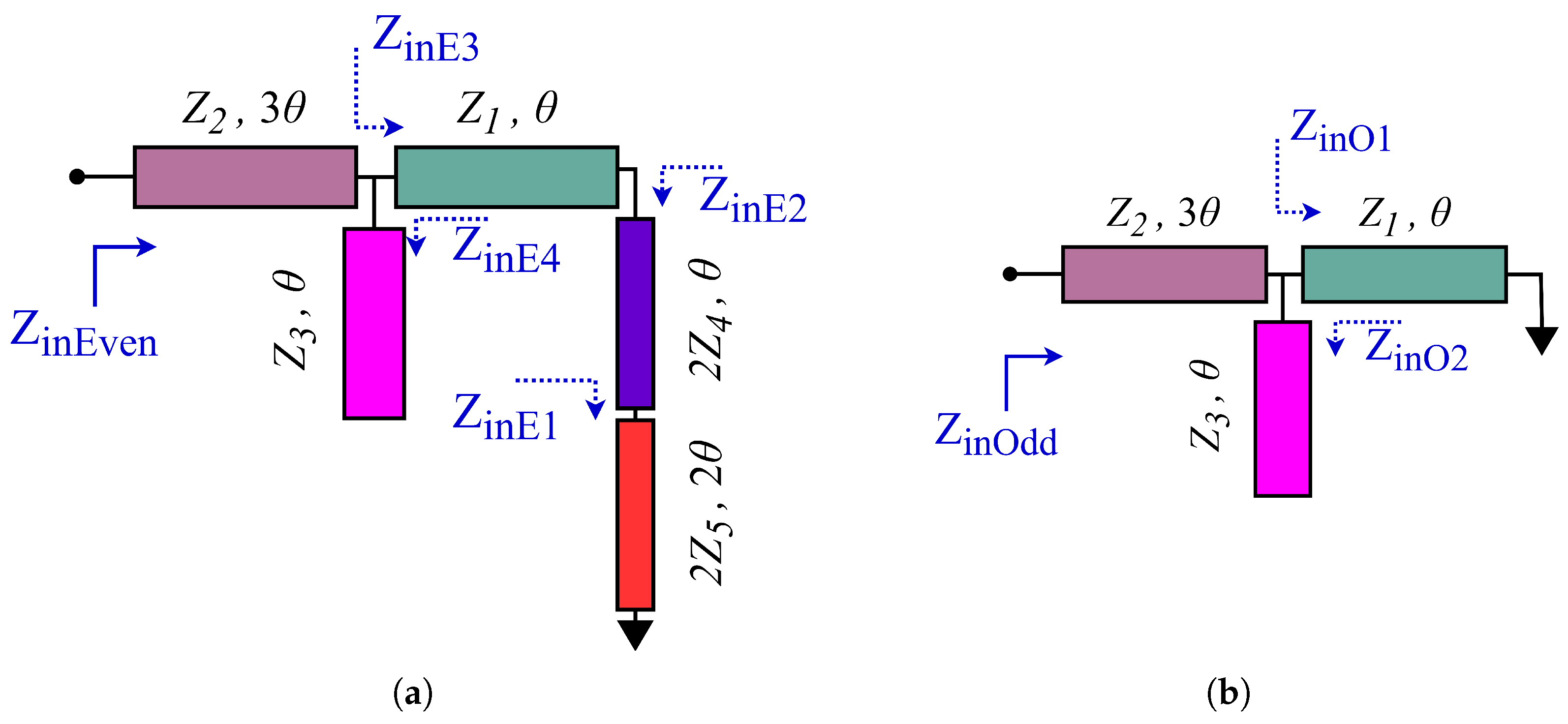
Figure 1 shows the equivalent transmission line model for the proposed MMR-based ultra-wideband bandpass filter, which comprises a couple of series transmission lines, open-circuit stubs, and short-circuit stubs. The central pair of transmission lines has the characteristic impedance Z 1 with an electrical length of θ , while the impedance Z 2 and the electrical length of 3 θ characterize the outermost pair. A shunt short-circuit stepped impedance transmission line is incorporated between the inner pair, which has the impedances Z 4 and Z 5 with electrical lengths θ and 2 θ , respectively. Furthermore, an open-circuited stub of electrical length θ and impedance Z 3 is connected in a shunt between the central and outer transmission lines. The proposed bandpass filter exhibits symmetry along the vertical plane. Therefore, filter performance metrics can be evaluated using even–odd-mode decomposition methods [2]. When an even (odd) mode is excited, a virtual open (short) circuit appears [2] along the vertical plane, and the equivalent filter circuits are demonstrated in Figure 2a and Figure 2b, respectively.
The input impedance of the even- and odd-mode circuit configurations can be obtained as follows:
Z i n E v e n = Z 2 Z L e + j Z 2 t a n 3 θ Z 2 + j Z L e t a n 3 θ
Z i n O d d = Z 2 Z L o + j Z 2 t a n 3 θ Z 2 + j Z L o t a n 3 θ
where Z L e and Z L o are indicated in Appendix A. The input impedances obtained in (1) and (2) are utilized to compute the even ( Γ E v e n ) and odd ( Γ O d d ) reflection coefficients and thus S parameters of the filter are as follows [2,33]:
Γ E v e n ( O d d ) = Z i n E v e n ( i n O d d ) Z o Z i n E v e n ( i n O d d ) + Z o
S 11 = 1 2 Γ E v e n + Γ O d d = Z i n E v e n Z i n O d d Z o 2 Z i n E v e n + Z o Z i n E v e n + Z o
S 21 = 1 2 Γ E v e n Γ O d d = Z i n E v e n Z i n O d d Z o Z i n E v e n + Z o Z i n E v e n + Z o
where Z o (= 50 Ω ) is the port reference impedance [2]. Note that the relationship between the center frequency ( f o ), arbitrary frequency (f), and the electrical length at the center frequency ( θ o ) is θ = θ o × ( f / f o ) [2]. The transmission zeros (i.e., frequencies at which the signal transmission is nullified) play a crucial role in shaping the filter frequency response. Therefore, three transmission zeros of the proposed filter are evaluated by solving S 21 = 0 and given in (6)–(8) as follows:
f T z 1 = 0
f T z 2 = f o θ o t a n 1 1 + 2 Z 5 Z 4
f T z 3 = f o θ 0 π 2
Note that the transmission zeros f T z 1 and f T z 3 are fixed, while f T z 2 can be adjusted with impedances Z 4 and Z 5 . As shown in Figure 3, when the impedance ratio Z 5 / Z 4 increases, the location of f T z 2 gradually departs from the center frequency ( f o ); thus, a higher bandwidth is expected at the expense of the selectivity factor, as will be clarified in Section 2.1. Furthermore, the variation in f T z 2 remains nearly constant for higher impedance ratios; therefore, Z 5 / Z 4 = 2.383 is considered, which maintains f T z 2 at 2.04 f o , achieving a wide bandwidth while maintaining better selectivity close to 1. The other values of Z 5 / Z 4 (i.e., f T z 2 > 2.04 f o ) can be chosen; however, the improvement in bandwidth is marginal and comes at the expense of a poorer selectivity factor and realization challenges.

2.1. The Analysis of Even- and Odd-Mode Resonances

The resonance behavior of the even- and odd-mode circuit topologies depicted in Figure 2 can be analyzed by identifying the frequencies where the input admittance becomes zero [2,28,30,40,41], as shown in Figure 4a. It confirms that the proposed bandpass filter circuit exhibits MMR behavior, with four even ( f e 1 , f e 2 , f e 3 , and f e 4 )- and three odd ( f o 1 , f o 2 , and f o 3 )-mode resonance frequencies. Furthermore, in Figure 4b the magnitude of insertion loss ( | S 21 | dB) under weak coupling has been plotted, which provides a clear visualization of even/odd frequencies, transmission zeros, and their significance in shaping the filter characteristics. The key observations are as follows:
  • The filter overall bandwidth is mainly characterized by two even-mode resonances f e 1 and f e 3 , while the mid-passband behavior can be modified by f o 1 , f e 2 , and f o 2 .
  • The largest bandwidth for a given Z 5 / Z 4 (i.e., the location of f T z 2 is known) is obtained when the even-mode resonances f e 1 and f e 3 simultaneously diverge from the center frequency ( f o ), i.e., f e 1 f T z 1 and f e 3 f T z 2 .
  • When f e 1 f T z 1 and f e 3 f T z 2 (i.e., when Z 4 and Z 5 are increased proportionally), the magnitude of S 21 at the lower and upper passband edges becomes steeper and higher selectivity is achieved.
  • The even mode f e 4 and the odd mode f o 3 present in the upper stopband can be suppressed by a transmission zero f T z 3 , and a wide stopband can be achieved.
The above analysis clarifies the importance of even/odd resonance frequencies in defining the filter passband and stopband characteristics. However, the role of Z 1 , Z 2 , Z 3 , Z 4 , and Z 5 on the resonance frequencies must be studied. Therefore, the locations of the three odd-mode frequencies f o 1 , f o 2 , and f o 3 are evaluated from the resonance condition Y i n O d d = 1 / Z i n O d d = 0 as given in (9)–(11):
f o 1 = f o θ o t a n 1 p 2 + p 2 2 4 p 1 p 3 2 p 1
f o 2 = f o θ o t a n 1 p 2 p 2 2 4 p 1 p 3 2 p 1
f o 3 = f o θ o π 2
where p 1 , p 2 and p 3 are indicated in Appendix B. Similarly, the position of the four even-mode frequencies f e 1 , f e 2 , f e 3 and f e 4 can be extracted by solving the resonance condition Y i n E v e n = 1 / Z i n E v e n = 0 as follows:
f e 1 = f o θ o t a n 1 γ c o s θ e + 2 π 3 b 3 a
f e 2 = f o θ o t a n 1 γ c o s θ e + 4 π 3 b 3 a
f e 3 = f o θ o t a n 1 γ c o s θ e + 6 π 3 b 3 a
f e 4 = f o θ 0 π 2
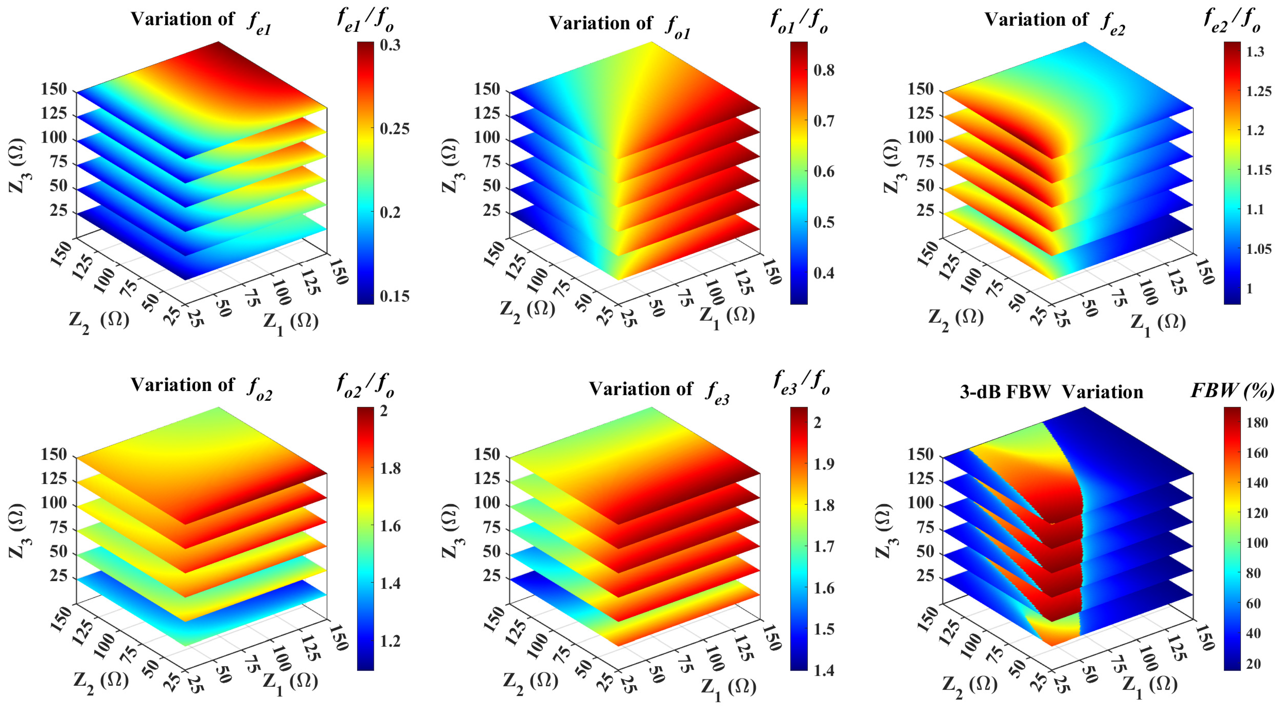
where γ , θ e , a, b, and c are given in Appendix B. It should be noted that transmission zero f T z 3 suppresses both the modes f o 3 and f e 4 appearing in the upper stopband, as they all occur at the same frequency (see (8), (11) and (15)). The complete visualization of passband even- and odd-mode resonance variations and their importance in achieving larger FBW is demonstrated in Figure 5. Note that the impedances of the shunt short-circuited stepped impedance line are set to Z 4 = 57.6 Ω and Z 5 = 137.28 Ω (with Z 5 / Z 4 = 2.383) to preserve the location of f T z 2 at 2.04 f o , and all other impedances Z 1 , Z 2 , and Z 3 are assumed to be within the practical realization limits (i.e., about 25 Ω –150 Ω for microstrip technology). It can be observed that the location of f e 1 remains closer to transmission zero f T z 1 , which is located at f T z 1 = 0 as can be seen from (6) (i.e., f e 1 0 ) when Z 1 is below 50 Ω and has minimal sensitivity to alteration in Z 2 and Z 3 for Z 1 lower than 50 Ω . Furthermore, f e 3 settles closer to f T z 2 = 2.04 f o (i.e., f e 3 2.04 f o ) when Z 2 is approximately below 55 Ω and is largely unaffected by variation in Z 1 and Z 3 for Z 2 roughly below 55 Ω . Therefore, it can be concluded collectively that when Z 1 and Z 2 have similar values in the lower range, both f e 1 and f e 3 are closely aligned with f T z 1 = 0 and f T z 2 = 2.04 f o , respectively. Thus, as expected, a 3 dB FBW of higher than 180% is obtained. Moreover, for a given Z 1 , Z 2 , and Z 3 , mid-passband resonances f o 1 , f e 2 , and f o 3 fall between the modes f e 1 and f e 3 , confirming that the 3 dB bandwidth is always governed by f e 1 and f e 3 . Therefore, to obtain the broader passband width of the proposed filter, the impedances Z 1 , Z 2 , and Z 3 are constrained within the approximate ranges 35 Ω Z 1 ≤ 55 Ω , 35 Ω Z 2 ≤ 55 Ω , and 60 Ω Z 3 ≤ 80 Ω , respectively. These values can be further fine-tuned to attain precise filter characteristics.

2.2. Impedance Fine-Tuning and Filter Ideal Performance

In this subsection, based on the comprehensive theoretical analysis presented above, the design methodology is first outlined, followed by a discussion of the filter’s ideal performance. The detailed step-by-step design procedure is summarized as follows.
  • Decide the center frequency f o of the filter.
  • Define the location of the transmission zero f T z 2 based on the bandwidth requirements (see Figure 3) and compute the impedance ratio Z 5 / Z 4 using (7). To achieve better selectivity, Z 4 and Z 5 must be maximized while maintaining the same ratio, considering the range of impedance values allowed by the fabrication process.
  • Finally, fine-tune the remaining impedances Z 1 , Z 2 , and Z 3 to obtain accurate filter characteristics.
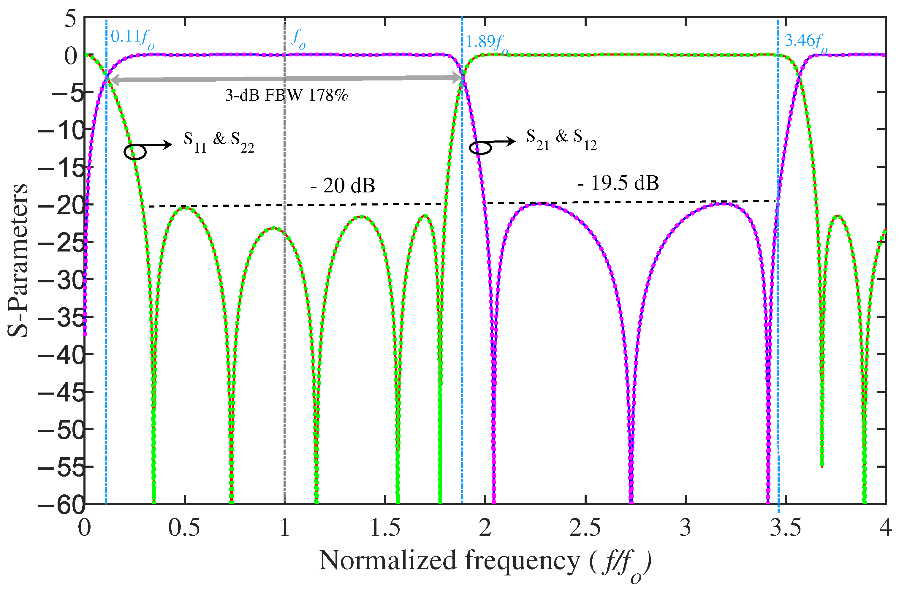
Based on the extensive theoretical analysis and the design procedure given above, an arbitrary center frequency f o is considered. The location of the transmission zero is set at f T z 2 = 2.04 f o , which eventually results in Z 5 / Z 4 = 2.383 (see Figure 3 or (7)). The optimum design parameters of the proposed bandpass filter are fine-tuned following the approach in [32] using the Advanced Design System (ADS) 2024 software and are reported in Table 1. Based on these electrical design parameters, the analytical S parameters of the proposed bandpass filter are extracted using (4) and (5) and plotted as a function of the normalized frequency ( f / f o ), as demonstrated in Figure 6. It is important to emphasize that these electrical design parameters are then used to determine the physical dimensions (i.e., lengths and widths) of the transmission line sections through the microstrip calculator, where the desired f o and material properties must also be specified, as will be addressed in Section 3. As can be seen in Figure 6, the ideal 3 dB passband bandwidth ranges from 0.11 f o to 1.89 f o with an FBW of 178%. Additionally, the RL is higher than 20 dB throughout the passband, which ranges from 0.28 f o to 1.8 f o . As for the stopband attenuation, it is higher than 19.5 dB and extends up to the 3.46 f o , showing excellent out-of-band rejection. Overall, as the proposed bandpass filter relies on a transmission line model with electrical length (i.e., a function of f o ) and impedances, it can be easily designed at any arbitrary center frequency f o , depending on the target applications.

3. Experimental Results and Discussion

This section addresses the fabrication, experimental verification, and performance analysis of the proposed MMR-based ultra-wideband bandpass filter. The ideal electrical design parameters, such as impedances and electrical lengths reported in Table 1, are utilized to calculate the length and width of every transmission line segment of the bandpass filter shown in Figure 1. The filter is designed to operate for ultra-wideband applications with a center frequency f o = 6.85 GHz. The filter is modeled and EM simulated using CST Studio Suite 2021, and manufactured on a Rogers RT/Duroid 5880 (Rogers Corporation, Chandler, AZ, USA) substrate with a thickness of 0.508 mm, a loss tangent (tan δ ) of 0.0009, and a dielectric constant ( ϵ r ) of 2.2. The final filter layout, including all dimensions and the fabricated filter prototype, is shown in Figure 7. Note that the short-shunt stepped impedance resonator is implemented in a 90° bent configuration to reduce the overall footprint area of the filter while maintaining its electrical characteristics. The total circuit area of the filter is only 23.46 × 8.27 mm2 (i.e., 0.79 λ g × 0.28 λ g , λ g being the guided wavelength at f o ), which is smaller than many alternative solutions in the literature, as will be detailed in the comparison in Table 2.
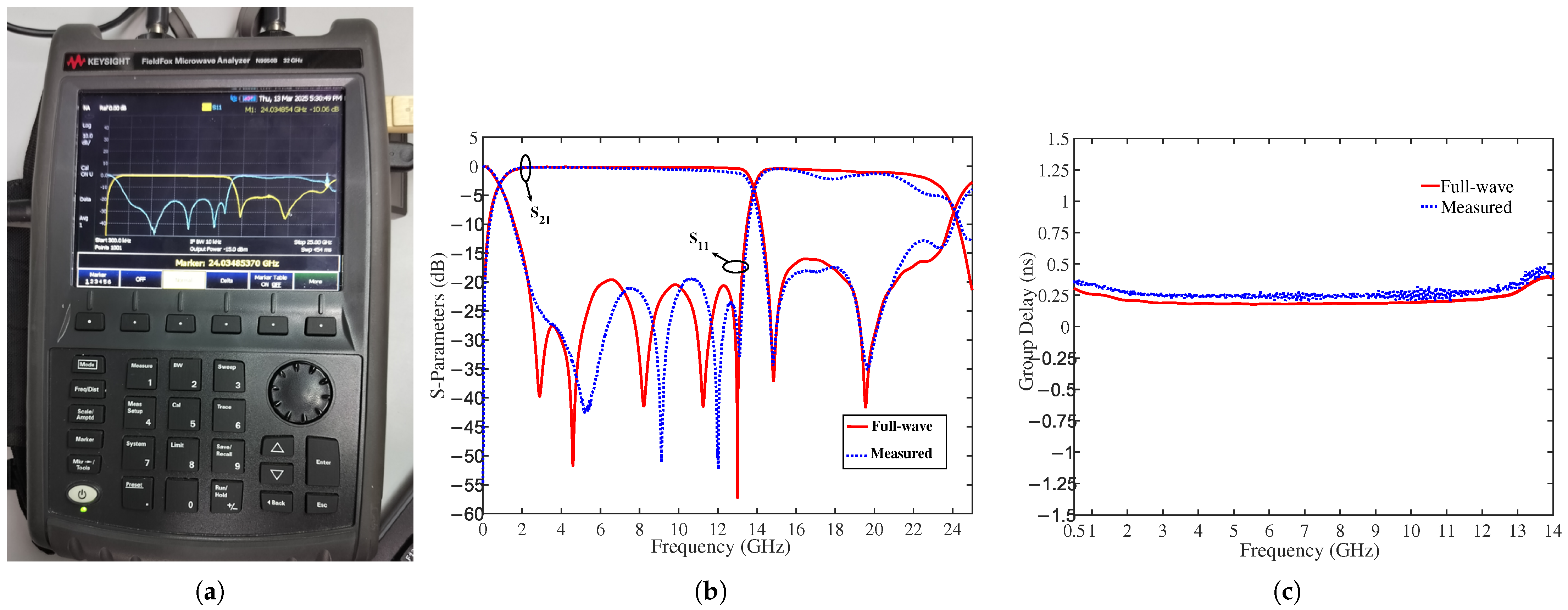
The prototype of the filter is tested using the Keysight FieldFox Microwave Analyzer N9950B 32 GHz (Santa Rosa, CA, USA), as shown in Figure 8a. The measured S parameters of the filter compared to the full-wave simulated results are represented in Figure 8b. As shown, the measured 3 dB passband bandwidth ranges from 0.85 to 13.65 GHz with an FBW of 176.6%, which is in good agreement with the full-wave simulation results, where the observed FBW is 176.16%, ranging from 0.87 to 13.76 GHz. Furthermore, the proposed bandpass filter achieves a measured (simulated) IL of 0.41 dB (0.19 dB) and an RL of 21.49 dB (22.3 dB) at the operating frequency f o = 6.85 GHz, whereas the RL is better than 19 dB throughout the passband, spanning from 2.25 to 13.32 GHz. The transmission zeros f T z 2 and f T z 3 appearing in the upper stopband are located at 14.83 GHz and 19.66 GHz, respectively. Thus, a wide stopband is achieved, which extends up to nearly 23.6 GHz (i.e., up to 3.44 f o ) with an attenuation level better than 14 dB. Additionally, the proposed filter maintains a flat group delay response throughout the passband, with a maximum variation of 0.25 ns (0.2 ns to 0.45 ns) in measurements and 0.21 ns (0.17 ns to 0.38 ns) in full-wave simulation, as shown in Figure 8c. This ensures the minimum distortion of the signal [42] and an accurate response in the time domain throughout the operational bandwidth, making the proposed bandpass filter a highly suitable candidate for very narrow pulse transmission/reception [43], such as RFID and radar systems. Furthermore, one of the important aspects of the proposed filter in real-life operation is its stable performance with respect to both temperature and input power. The use of a Rogers RT/duroid 5880 ensures excellent thermal stability, while the distributed microstrip line configuration provides high RF power handling capability. Therefore, the proposed filter design is robust and reliable for integration in practical scenarios where consistent performance under varying environmental and operating conditions is essential, such as aerospace systems, radar front ends, and high-power wireless links. Finally, it is important to note that the minor discrepancies between the measured and full-wave simulated results could be due to imperfections in the measurement setup, fabrication tolerances, connectors/cables, soldering, etc.
The detailed comparison between the proposed ultra-wideband bandpass filter and the current state-of-the-art works is reported in Table 2. As can be seen, the proposed bandpass filter exhibits an extremely wide bandwidth while being implemented using traditional printed circuit board (PCB) technology, demonstrating substantial improvement over the existing HTS, multilayered, and conventional PCB technology-based filter designs. Furthermore, the proposed bandpass filter outperforms existing designs in terms of RL, IL, SF, and stopband harmonic suppression. Although the design proposed in [18] achieves a comparable FBW, it exhibits poor RL and IL performance, and it depends on multilayer technology, eventually leading to complex fabrication procedures and higher costs. In addition, filter designs that utilize HTS technology [21,22,23,31] require specialized materials such as DyBCO and YBCO to be coated on MgO substrates, making them expensive due to the complex manufacturing procedure.

Figure of Merit

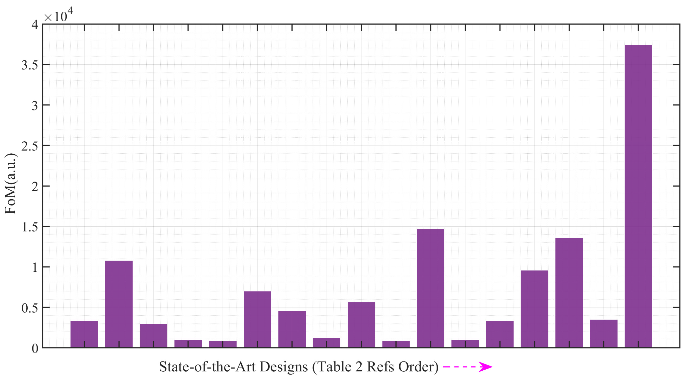
The primary goal of the proposed bandpass filter is to achieve an extremely wide bandwidth while maintaining a high SF, low IL, high RL, and a flat group delay using printed circuit board (PCB) technology (i.e., microstrip technology). Additionally, the proposed filter exhibits stopband rejection up to 3.44 f o , which outperforms most of the designs reported in the state-of-the-art literature. Indeed, the stopband attenuation level is 14 dB, which is better than the commonly accepted threshold of 10 dB [2,43,44], ([35] Figure 10). A figure of merit (FoM) has been introduced that gives the best trade-off between key filter parameters such as FBW, RL, IL, SF, and group delay flatness as follows:
FoM ( a . u . ) = FBW ( % ) × 10 RL / 20 × SF 10 IL / 20 × ( G D ) max ( G D ) min × f o ( GHz )
where GD is the group delay in nanoseconds, and when the difference ( G D ) m a x ( G D ) m i n approaches zero, it ensures a flat group delay response of the filter, which is desirable to achieve lower signal distortion or narrow pulse transmission/reception. Furthermore, it is important to note that the multiplication of f o ensures that the FoM fairly accounts for increased design challenges at high frequencies, such as parasitic effects, dielectric losses, fabrication difficulties, etc. The FoM lies in the interval ( 0 , ) , and the larger the FoM, the better the trade-off between the filter performance parameters. Accordingly, the FoM has been evaluated using (16), and the corresponding values are presented in the bar chart depicted in Figure 9. As can be seen, the proposed ultra-wideband bandpass filter achieves the highest FoM, representing the best trade-off among the FBW, IL, RL, SF, and flat group delay response compared to the state-of-the-art designs reported in Table 2. Overall, the proposed bandpass filter surpasses the state-of-the-art designs in performance, size, cost, and complexity; thus, it is a potential candidate for ultra-wideband communication systems.

4. Conclusions

In this study, a novel configuration of an MMR-based ultra-wideband bandpass filter has been proposed and experimentally verified. The proposed filter topology comprises a short-circuited shunt-stepped-impedance resonator and shunt-open-circuited stubs, exhibiting symmetry in the vertical plane. Thus, the even and odd decomposition methods are employed to obtain closed-form expressions for even/odd resonance frequencies, transmission zeros, and scattering parameters, which are essential for analyzing the filter performance metrics, thereby establishing a robust theoretical framework. The filter has been prototyped using microstrip technology and outperforms state-of-the-art designs. Additionally, the proposed filter maintains a flat group delay response throughout the passband, with a maximum variation of 0.25 ns (0.2 ns to 0.45 ns) in measurements and 0.21 ns (0.17 ns to 0.38 ns) in full-wave simulation. This ensures minimal signal distortion and an accurate time-domain response throughout the operational bandwidth, making the proposed bandpass filter a highly suitable candidate for very narrow pulse transmission/reception, such as UWB communication, radar systems, and RFID reader systems.
As the proposed bandpass filter is based on a transmission line model with electrical length (as a function of frequency) and impedances, it can be easily scaled to other frequencies depending on the target applications, especially up to a few GHz. Nevertheless, the absence of additional transmission zeros in the lower stopband may degrade the selectivity factor at higher frequencies, which we will consider in our future investigations.

Author Contributions

Conceptualization, R.R. and D.R.; methodology, R.R., R.K.B., and D.R.; software, R.R.; validation, R.R., D.R., and G.C.; formal analysis, S.K., G.C., S.G., and D.R.; investigation, R.R. and D.R.; resources, D.R.; data curation, R.R. and D.R.; writing—original draft preparation, R.R.; writing—review and editing, G.C., S.K., S.G., and D.R.; visualization, R.K.B., G.C., and D.R.; supervision, D.R. and S.G.; project administration, D.R.; funding acquisition, D.R. All authors have read and agreed to the published version of the manuscript.

Funding

This research received no external funding.

Data Availability Statement

Data will be available on a reasonable request from the authors.

Acknowledgments

This work is partially supported by the Italian Ministry of University and Research (MUR) in the framework of the CrossLab and FoReLab projects (Departments of Excellence), Department of Information Engineering, University of Pisa, Italy.

Conflicts of Interest

The authors declare no conflict of interest.

Appendix A

The even- and odd-mode input impedances given in (1) and (2) must be evaluated using a set of intermediate impedance expressions. These are obtained using the transmission line theory [2]. The Z L e in (1) can be expressed as follows:
Z L e = Z i n E 3 Z i n E 4 Z i n E 3 + Z i n E 4
Z i n E 4 = j Z 3 c o t θ
Z i n E 3 = Z 1 Z i n E 2 + j Z 1 t a n θ Z 1 + j Z i n E 2 t a n θ
Z i n E 2 = 2 Z 4 Z i n E 1 + j 2 Z 4 t a n θ 2 Z 4 + j Z i n E 1 t a n θ
Z i n E 1 = j 2 Z 5 t a n 2 θ
Similarly, the expressions for the Z L o in (2) can be written as follows:
Z L o = Z i n O 1 Z i n O 2 Z i n O 1 + Z i n O 2
Z i n O 2 = j Z 3 c o t θ
Z i n O 1 = j Z 1 t a n θ

Appendix B

The following intermediate expressions are used to compute the location of the even- and odd-mode resonance frequencies. Thus, p 1 , p 2 , and p 3 in (9)–(11) is as follows:
p 1 = 3 Y 2 Y 3 + Y 2 2
p 2 = Y 2 Y 3 + 3 Y 1 Y 2 + 3 Y 2 2
p 3 = Y 1 Y 2
The expressions for γ , θ e , a, b, and c in (12)–(15) is as follows:
γ = 2 P 3 , θ e = c o s 1 3 Q 2 P 3 P
P = 3 a c b 2 3 a 2 , Q = 2 b 3 9 a b c + 27 a 2 d 27 a 3
a = 3 k 11 + Y 2 k 9 , b = k 11 + 3 k 10 + 3 Y 2 k 9 + Y 2 k 8
c = k 10 + 3 k 5 + 3 Y 2 k 8 , d = k 1 Y 1
k 1 = 0.5 Y 4 Y 5 , k 2 = 0.5 Y 4 Y 5 + 2 Y 4 , k 3 = 2 Y 4 + Y 5
k 4 = Y 5 , k 5 = k 1 Y 1 , k 6 = Y 1 k 2 + Y 1 k 3
k 7 = Y 1 2 k 4 , k 8 = Y 1 k 3 + k 1 , k 9 = Y 1 k 4 + k 2
k 10 = Y 3 k 8 + k 6 , k 11 = Y 3 k 9 + k 7
In (A9)–(A19), the admittances are defined as Y i = 1 / Z i for i = 1 , 2 , 3 , 4 , 5 (i.e., the admittance is simply the reciprocal of its corresponding impedance).

References

  1. Aiello, G.; Rogerson, G. Ultra-wideband wireless systems. IEEE Microw. Mag. 2003, 4, 36–47. [Google Scholar] [CrossRef]
  2. Pozar, D.M. Microwave Engineering: Theory and Techniques; John Wiley & Sons: Hoboken, NJ, USA, 2021. [Google Scholar]
  3. Hsu, C.L.; Hsu, F.C.; Kuo, J.K. Microstrip bandpass filters for Ultra-Wideband (UWB) wireless communications. In Proceedings of the IEEE MTT-S International Microwave Symposium Digest, Long Beach, CA, USA, 17 June 2005; pp. 679–682. [Google Scholar] [CrossRef]
  4. Tang, C.W.; Chen, M.G. A Microstrip Ultra-Wideband Bandpass Filter with Cascaded Broadband Bandpass and Bandstop Filters. IEEE Trans. Microw. Theory Tech. 2007, 55, 2412–2418. [Google Scholar] [CrossRef]
  5. Ramkumar, S.; Anitha, M.; Boopathi Rani, R.; Muthuramya, C. Compact Ultra-Wide-Stopband Microwave Bandpass Filter with Multiple Transmission Zeros by Integrating an L-Shaped Bandpass Filter and a Stepped Impedance Lowpass Filter. IEEE Lat. Am. Trans. 2025, 23, 437–443. [Google Scholar] [CrossRef]
  6. Lee, J.K.; Kim, Y.S. Ultra-Wideband Bandpass Filter with Improved Upper Stopband Performance Using Defected Ground Structure. IEEE Microw. Wirel. Compon. Lett. 2010, 20, 316–318. [Google Scholar] [CrossRef]
  7. Xie, J.; Tang, D.; Shu, Y.; Luo, X. Compact UWB BPF with Broad Stopband Based on Loaded-Stub and C-Shape SIDGS Resonators. IEEE Microw. Wirel. Compon. Lett. 2022, 32, 383–386. [Google Scholar] [CrossRef]
  8. Song, Y.; Yang, G.M.; Geyi, W. Compact UWB Bandpass Filter with Dual Notched Bands Using Defected Ground Structures. IEEE Microw. Wirel. Compon. Lett. 2014, 24, 230–232. [Google Scholar] [CrossRef]
  9. Breed, G. An introduction to defected ground structures in microstrip circuits. High Freq. Electron. 2008, 7, 50–54. [Google Scholar]
  10. Wang, H.; Zhu, L.; Menzel, W. Ultra-wideband bandpass filter with hybrid microstrip/CPW structure. IEEE Microw. Wirel. Compon. Lett. 2005, 15, 844–846. [Google Scholar] [CrossRef]
  11. Thomson, N.; Hong, J.S. Compact Ultra-Wideband Microstrip/Coplanar Waveguide Bandpass Filter. IEEE Microw. Wirel. Compon. Lett. 2007, 17, 184–186. [Google Scholar] [CrossRef]
  12. Ghazali, A.N.; Sazid, M.; Virdee, B. A compact UWB-BPF based on microstrip-to-CPW transition with multiple transmission zeros. Microw. Opt. Technol. Lett. 2018, 60, 1925–1928. [Google Scholar] [CrossRef]
  13. Zheng, Y.; Wang, W.; Wu, Y. Synthesis of High-Selectivity Ultra-Wideband Reflective/Absorptive Bandpass Filters with Unequal-Width Three-Coupled Line Sections. IEEE Trans. Circuits Syst. II Express Briefs 2023, 70, 1961–1965. [Google Scholar] [CrossRef]
  14. Zhang, Z.; Zhang, G.; Tam, K.W.; Zhou, X.; Chen, S. Millimeter-Wave On-Chip Ultrawideband Bandpass Filter on Coupled Line Based Bi-Path Topology Using GaAs Technology. IEEE Trans. Compon. Packag. Manuf. Technol. 2025, 15, 553–559. [Google Scholar] [CrossRef]
  15. Makimoto, M.; Yamashita, S. Bandpass Filters Using Parallel Coupled Stripline Stepped Impedance Resonators. IEEE Trans. Microw. Theory Tech. 1980, 28, 1413–1417. [Google Scholar] [CrossRef]
  16. Shome, P.P.; Khan, T.; Koul, S.K.; Antar, Y.M. Two Decades of UWB Filter Technology: Advances and Emerging Challenges in the Design of UWB Bandpass Filters. IEEE Microw. Mag. 2021, 22, 32–51. [Google Scholar] [CrossRef]
  17. Li, M.; Yang, Y.; Iacopi, F.; Yamada, M.; Nulman, J. Compact Multilayer Bandpass Filter Using Low-Temperature Additively Manufacturing Solution. IEEE Trans. Electron Devices 2021, 68, 3163–3169. [Google Scholar] [CrossRef]
  18. Wang, M.; Sun, S.; Ma, H.F.; Cui, T.J. Supercompact and Ultrawideband Surface Plasmonic Bandpass Filter. IEEE Trans. Microw. Theory Tech. 2020, 68, 732–740. [Google Scholar] [CrossRef]
  19. Yang, L.; Zhu, L.; Zhang, R.; Wang, J.; Choi, W.W.; Tam, K.W.; Gómez-García, R. Novel Multilayered Ultra-Broadband Bandpass Filters on High-Impedance Slotline Resonators. IEEE Trans. Microw. Theory Tech. 2019, 67, 129–139. [Google Scholar] [CrossRef]
  20. Wu, C.H.; Lin, Y.S.; Wang, C.H.; Chen, C.H. A compact LTCC ultra-wideband bandpass filter using semi-lumped parallel-resonance circuits for spurious suppression. In Proceedings of the 2007 European Microwave Conference, Munich, Germany, 9–12 October 2007; pp. 532–535. [Google Scholar] [CrossRef]
  21. Tian, H.; Liu, H. Miniaturized Ultra-Wideband HTS Bandpass Filter Using High-Q CRLH Transmission Line. IEEE Trans. Circuits Syst. II Express Briefs 2024, 71, 2599–2603. [Google Scholar] [CrossRef]
  22. Long, Z.; Tian, M.; Zhang, T.; Qiao, M.; Wu, T.; Lan, Y. High-Temperature Superconducting Multimode Dual-Ring UWB Bandpass Filter. IEEE Trans. Appl. Supercond. 2020, 30, 1500204. [Google Scholar] [CrossRef]
  23. Dai, J.; Wu, Y.; Yuan, Y.; Wang, X.; Zhang, C.; Wang, J.; Li, G.; Li, C.; Sun, L.; Luo, S.; et al. HTS Wideband Bandpass Filter Based on Ladder Topology Circuit and Microstrip Transformation. IEEE Trans. Appl. Supercond. 2021, 31, 1501007. [Google Scholar] [CrossRef]
  24. Zhu, L.; Sun, S.; Menzel, W. Ultra-wideband (UWB) bandpass filters using multiple-mode resonator. IEEE Microw. Wirel. Compon. Lett. 2005, 15, 796–798. [Google Scholar] [CrossRef]
  25. Wang, H.; Chu, Q.X.; Gong, J.Q. A Compact Wideband Microstrip Filter Using Folded Multiple-Mode Resonator. IEEE Microw. Wirel. Compon. Lett. 2009, 19, 287–289. [Google Scholar] [CrossRef]
  26. Nosrati, M.; Mirzaee, M. Compact Wideband Microstrip Bandpass Filter Using Quasi-Spiral Loaded Multiple-Mode Resonator. IEEE Microw. Wirel. Compon. Lett. 2010, 20, 607–609. [Google Scholar] [CrossRef]
  27. Weng, M.H.; Liauh, C.T.; Wu, H.W.; Vargas, S.R. An Ultra-Wideband Bandpass Filter with an Embedded Open-Circuited Stub Structure to Improve In-Band Performance. IEEE Microw. Wirel. Compon. Lett. 2009, 19, 146–148. [Google Scholar] [CrossRef]
  28. Song, K.; Xue, Q. Inductance-Loaded Y-Shaped Resonators and Their Applications to Filters. IEEE Trans. Microw. Theory Tech. 2010, 58, 978–984. [Google Scholar] [CrossRef]
  29. Zhang, Z.; Xiao, F. An UWB Bandpass Filter Based on a Novel Type of Multi-Mode Resonator. IEEE Microw. Wirel. Compon. Lett. 2012, 22, 506–508. [Google Scholar] [CrossRef]
  30. Ahmed, K.U.; Virdee, B.S. Ultra-Wideband Bandpass Filter Based on Composite Right/Left Handed Transmission-Line Unit-Cell. IEEE Trans. Microw. Theory Tech. 2013, 61, 782–788. [Google Scholar] [CrossRef]
  31. Zhang, T.; Tian, M.; Long, Z.; Qiao, M.; Fu, Z. High-Temperature Superconducting Multimode Ring Resonator Ultrawideband Bandpass Filter. IEEE Microw. Wirel. Compon. Lett. 2018, 28, 663–665. [Google Scholar] [CrossRef]
  32. Sheikhi, A.; Alipour, A.; Mir, A. Design and Fabrication of an Ultra-Wide Stopband Compact Bandpass Filter. IEEE Trans. Circuits Syst. II Express Briefs 2020, 67, 265–269. [Google Scholar] [CrossRef]
  33. Kanaparthi, V.P.K.; Velidi, V.K.; Rajkumar, R.; Rama Rao, T. A Compact Ultra-Wideband Multimode Bandpass Filter with Sharp-Rejection Using Stepped Impedance Open Stub and Series Transformers. IEEE Trans. Circuits Syst. II Express Briefs 2022, 69, 4824–4828. [Google Scholar] [CrossRef]
  34. Tang, C.W.; Chen, C.A. Analysis and Design of Planar Extremely-Wideband Bandpass Filter with Broad Stopband Performance. IEEE Access 2024, 12, 131785–131793. [Google Scholar] [CrossRef]
  35. Bandyopadhyay, A.; Sarkar, P.; Ghatak, R. A Bandwidth Reconfigurable Bandpass Filter for Ultrawideband and Wideband Applications. IEEE Trans. Circuits Syst. II Express Briefs 2022, 69, 2747–2751. [Google Scholar] [CrossRef]
  36. Rajender, R.; Ciarpi, G.; Genovesi, S.; Rossi, D. Design of an Ultra-wideband Multiple-Mode Resonator (MMR)-Based High Selectivity Bandpass Filter. In Applications in Electronics Pervading Industry, Environment and Society, Proceedings of the ApplePies 2024, Turin, Italy, 19–20 September 2024; Lecture Notes in Electrical Engineering; Springer: Cham, Switzerland, 2024; Volume 1369, pp. 304–312. [Google Scholar]
  37. Zeng, J.; Li, X.; Qi, Z. UWB bandpass filter with compact size and wide upper stopband. Microw. Opt. Technol. Lett. 2020, 62, 1521–1525. [Google Scholar] [CrossRef]
  38. Zhou, C.X.; Guo, P.P.; Zhou, K.; Wu, W. Design of a Compact UWB Filter with High Selectivity and Superwide Stopband. IEEE Microw. Wirel. Compon. Lett. 2017, 27, 636–638. [Google Scholar] [CrossRef]
  39. Nadeem, A.; Shoaib, N.; Papadakis, A.; Nikolaou, S.; Psychogiou, D.; Vryonides, P. Advanced Techniques for Designing Wideband and Highly Selective Bandpass Filters Through Cascaded Modules. IEEE Access 2025, 13, 34936–34945. [Google Scholar] [CrossRef]
  40. Xie, Y.; Chen, F.C.; Li, Z. Design of Dual-Band Bandpass Filter with High Isolation and Wide Stopband. IEEE Access 2017, 5, 25602–25608. [Google Scholar] [CrossRef]
  41. Krishna, I.S.; Barik, R.K.; Karthikeyan, S.S. A miniaturized wideband bandpass filter based on 3λ/4 resonator loaded with stepped impedance. In Proceedings of the 2017 Twenty-Third National Conference on Communications (NCC), Chennai, India, 2–4 March 2017; pp. 1–5. [Google Scholar] [CrossRef]
  42. Psychogiou, D.; Gómez-García, R.; Peroulis, D. Constant In-Band Group-Delay Acoustic-Wave-Lumped-Element-Resonator-Based Bandpass Filters and Diplexers. IEEE Trans. Microw. Theory Tech. 2018, 66, 2199–2209. [Google Scholar] [CrossRef]
  43. Abbosh, A.M. Planar Bandpass Filters for Ultra-Wideband Applications. IEEE Trans. Microw. Theory Tech. 2007, 55, 2262–2269. [Google Scholar] [CrossRef]
  44. Qian, S.; Hong, J. Miniature Quasi-Lumped-Element Wideband Bandpass Filter at 0.5–2-GHz Band Using Multilayer Liquid Crystal Polymer Technology. IEEE Trans. Microw. Theory Tech. 2012, 60, 2799–2807. [Google Scholar] [CrossRef]
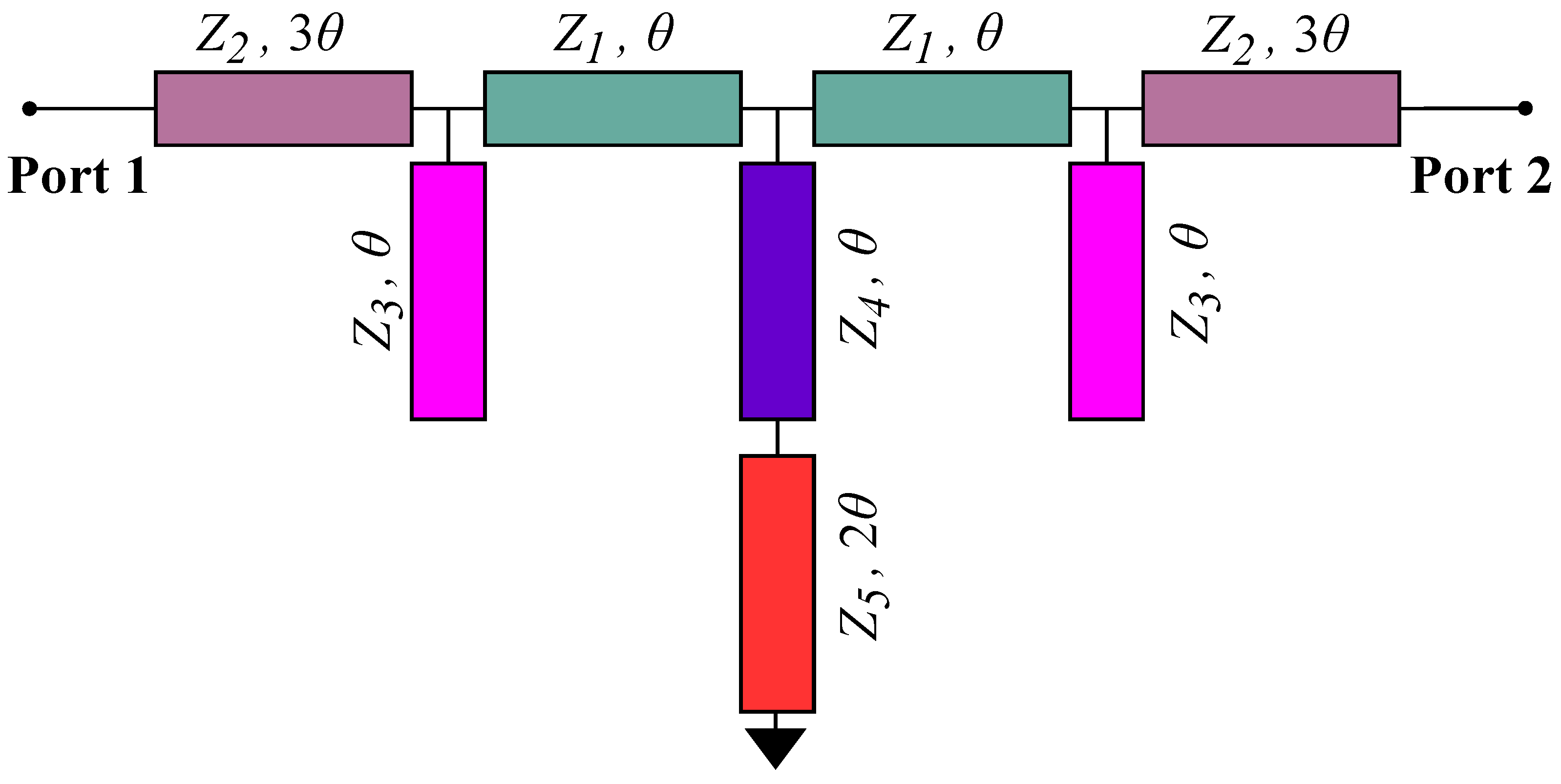
Figure 1. The proposed multi-mode resonator-based ultra-wideband bandpass filter transmission line model.
Electronics 14 03992 g001
Figure 2. The equivalent (a) even-mode and (b) odd-mode circuit topologies of the proposed filter.
Electronics 14 03992 g002
Figure 3. The location of transmission zeros as a function of impedance ratio Z 5 / Z 4 .
Electronics 14 03992 g003
Figure 4. Proposed bandpass filter demonstrating multiple (a) even–odd mode resonances and (b) magnitude of the insertion loss ( | S 21 | dB) under a weak coupling.
Electronics 14 03992 g004
Figure 5. The variation of even/odd-mode frequencies and 3 dB fractional bandwidth as a function of Z 1 , Z 2 , and Z 3 ( Z 4 = 57.6 Ω and Z 5 = 137.28 Ω are considered).
Electronics 14 03992 g005
Figure 6. The ideal S parameters of the proposed ultra-wideband bandpass filter.
Electronics 14 03992 g006
Figure 7. The proposed bandpass filter (a) layout with dimensions and (b) fabricated prototype.
Electronics 14 03992 g007
Figure 8. An illustration of (a) a measurement setup, (b) a comparison between the measured and full-wave simulated results, and (c) a group delay response.
Electronics 14 03992 g008
Figure 9. The figure of merit (FoM) comparison between the proposed ultra-wideband bandpass filter (this work, right last bar) and state-of-the-art designs [5,7,13,18,19,21,22,23,30,31,32,33,34,35,37,38], presented in the same order as in Table 2.
Electronics 14 03992 g009
Table 1. Final design parameters of the proposed MMR-based bandpass filter.
Parameter Z 1 Z 2 Z 3 Z 4 Z 5 θ | f 0
Value47.09 Ω 42.20 Ω 71.88 Ω 57.60 Ω 137.28 Ω 33°
Table 2. Comprehensive comparison between the proposed ultra-wideband bandpass filter and the state-of-the-art literature.
 Ref.   f o
(GHz) 
 FBW
(%) 
IL
(dB)
RL
(dB)
SF
 
Group Delay
(ns)
HSSize
( λ g × λ g )
MLFilt. Conf./Fabr. Pro.
[5]2.10140.40.8>15.0N/A0.4 e–0.814.3 f o (22.5 dB)0.23 × 0.37NoBPF + LPF/Conv. PCB
[7]6.85114.00.60>14.0N/A0.30–0.609.70 f o (26 dB)  0.354 × 0.302  YesSIDGS Res./ML-PCB
[13]3.04110.30.79>12.9N/A0.60–2.002.53 f o (18.7 dB)0.70 × 0.30NoUWTCL/Conv. PCB
[18]2.40174.01.10>11.0N/A0.90–2.062.91 f o (20 dB)1.30 × 0.19YesSSPP/ML-PCB
[19]2.001133.70.65>13.6N/A1.23 m i v 2.09 f o (10 dB)0.8 × 0.51YesHISL Res./ML-PCB
[21]6.0073.00.18>17.80.840.5 e–0.902.0 f o (22 dB)0.07 × 0.23No High-Q CRLH-TL/HTS-PCB
[22]6.85125.30.42>15.20.870.16–1.062.33 f o (20 dB)1.57 × 1.18No Dual-Ring Res./HTS-PCB
[23]1.75108.00.29>14.0N/AN/A2.28 f o (40 dB)0.73 × 0.47No LPF-Derived BPF/HTS-PCB
[30]6.82115.00.50>11.00.860.10–0.502.34 f o (18 dB)0.56 × 0.16NoCRLH-TL/Conv. PCB
[31]4.04122.30.75>10.70.910.19–1.782.22 f o (20 dB)1.53 × 0.45No Ring-MMR/HTS-PCB
[32]6.9597.00.42>19.0N/A0.025–0.37 +4.31 * f o (24 dB)0.128 × 0.378NoTwo 5-Stage SIRs/Conv. PCB
[33]2.49103.20.87>15.00.930.99–2.202.20 f o (25 dB)0.165NoSIOS & ST/Con. PCB
[34]4.50155.60.72>13.5N/A0.60 e–1.408.9 f o (30 dB)0.60 × 0.44NoMSCLP/Conv. PCB
[35]6.80132.81.60>10.0N/A0.68–0.902.72 f o (12 dB)0.80 × 0.42NoOSSLR-SSSLR/Conv. PCB
[37]6.85110.90.9>13.0N/A0.2–0.404.38 f o (18 dB)0.22 × 0.20NoCRLH-TL/Conv. PCB
[38]6.85110.11.6>12.00.92N/A3.50 * f o (15 dB)0.60 × 0.54NoHM-SIW + EBG/SIW-PCB
T.W.6.85176.60.33>19.30.870.20–0.453.44 f o (14 dB)0.79 × 0.28NoSSSIS & SOS/Conv. PCB
T.W.: This work; FBW: 3 dB fractional bandwidth; IL: insertion loss; RL: return loss; selectivity factor (SF) = Δ 3 dB / Δ 30 dB ; HS: harmonic suppression; ML: multilayer; λ g : guided wavelength at f o ; *: measured; +: simulated; m i v : maximum in-band variation; e: estimation; HTS: high-temperature superconducting; : dielectric with HTS films, higher cost and complex fabrication process; PCB: printed circuit board; LPF: low-pass filter; BPF: bandpass filter; SIDGS: substrate-integrated defected ground structure; Res.: resonators; UWTCL: unequal-width three-coupled line; SSPP: spoof surface plasmonic polariton; HISL: high-impedance slotline; Q: quality factor; CRLH: composite right-/left-handed; TL: transmission line; MMR: multi-mode resonator; SIR: stepped impedance resonators; SIOS & ST: stepped impedance open stub and series transformers; MSCLP: modified short-circuited coupled-line pairs; OSSLR-SSSLR: open stepped impedance stub-loaded resonator–shorted stepped impedance stub-loaded resonator; HM-SIW: half-mode substrate-integrated waveguide; SSSIS & SOS (Proposed): short shunt-stepped impedance stubs, and shunt-open stubs.
Disclaimer/Publisher’s Note: The statements, opinions and data contained in all publications are solely those of the individual author(s) and contributor(s) and not of MDPI and/or the editor(s). MDPI and/or the editor(s) disclaim responsibility for any injury to people or property resulting from any ideas, methods, instructions or products referred to in the content.