Article

Spatial Monitoring of I/O Interconnection Nets in Flip-Chip Packages

Department of Electrical and Electronic Engineering, Ariel University, Ariel 40700, Israel
*
Author to whom correspondence should be addressed.
Electronics 2025, 14(17), 3549; https://doi.org/10.3390/electronics14173549 (registering DOI)
Submission received: 18 July 2025 / Revised: 1 September 2025 / Accepted: 3 September 2025 / Published: 6 September 2025
(This article belongs to the Special Issue Advances in Hardware Security Research)

Abstract

Here, we introduce a novel method for the real-time spatial monitoring of I/O interconnection nets in flip-flop packages. Resistance changes in 39 I/O nets are observed simultaneously to produce a spatial profile of the relative degradations of the solder ball joints, interconnection lines, and transistor gates. Location-specific TTF profiles are generated from the degradation data to show the impact of the I/O nets in the context of their placement on the chip. The system succeeds in formulating a clear trend of resistance increase even in relatively mild constant temperature stress conditions. Test results of four temperatures from 80 °C to 120 °C show a dominant degradation pattern strongly influenced by BTI aging demonstrating an acute vulnerability in the pass gates to voltage and temperature stress. The proposed compact spatial monitor solution can be integrated into virtually all chip orientations. The outcome of this study can assist in foreseeing system vulnerabilities in a large spectrum of packaging and advanced packaging orientations in field applications.

1. Introduction

1.1. Spatial Monitoring in Microchips

The demand for microchip prognostics is escalating with new trends in complex integrated circuit (IC) development. The advancement of artificial intelligent (AI)-based solutions is increasing the thirst for augmented compute-power. These applications are driving devices to levels of dynamic power consumption beyond anything known to date. Society is becoming more dependent on AI solutions, and, therefore, they must be failsafe.
The topic of prognostics in all forms of electronics systems originated in critical mission systems including automotive, aviation, and space systems [1,2,3]. As with virtually all services in our society today, microchip prognostics occupy a large portion of semiconductor planning and development. Many solutions have been proposed. Among them are periodic built in self-tests (BIST) to verify functionality of systems over time and remaining useful life [RUL] detectors to assess field product lifetimes [4,5,6].
One form of prognostic systems relatively underrepresented is spatial monitoring in the chip. Spatial sensory is challenging because it expends resources and is hard to implement. Structural sensors have been proposed in several forms including piezoelectric sensors tuned to detect Lamb wave propagation in the plates [7,8,9,10]. Although this approach is effective at finding cracks and structural vulnerabilities, the functionality of the chip may be impaired preceding this damage.
Our study proposes a method for monitoring performance degradation in microchips with location-specific monitors. The approach includes a novel measuring procedure finding the resistance shift of I/O nets over a large area of the chip. The I/O nets follow through the ball grid array (BGA) into interconnects and enter the FPGA through pass gates. Resistance shift is the summation of degradation causes in the net. Monitoring the I/O nets is an effective way to find the location specific RUL of the device and reveal vulnerable areas due to design deficiencies and stress pockets in the chip.

1.2. Common Vulnerabilities and Failures in BGAs, Interconnects, and Pass Gate Transistors

Some major issues are mentioned in this section. A comprehensive review is beyond the scope of the work. Since electronics devices consist of a large range of materials including metals, composites, polymers, and ceramics, the thermal expansion of the materials is prone to cause various damages. In BGA structures, shear strain will stress the solder joints. Solder joints are subjected to mechanical stresses and strains due to the mismatch of coefficients of thermal expansion (CTE) between the different materials [11]. When devices are subjected to extreme thermal conditions, the consequence is acute shear stress. Solder joint fractures are manifested in three major modes: pad matrix failure, bulk solder failure, and intermetallic compounds (IMC) failures. Changes in resistance can attest to solder joint fatigue at the level of single milliohms [12,13]. The results of this work show much larger resistance shifts that suggest dominant degradation from a different source.
Electromigration is also a critical failure mechanism in solder joints and interconnects [14]. Extensive studies have been performed on EM in solder joints and solder lines. The studies reveal MTTF of electromigration on two structures: a flip-chip solder/under-bump metallization (UBM) structure and a 3D multilevel aluminum or copper via/wiring structure [15,16]. Further studies show the deprivation of EM in interconnects [17].
Possibly the most influential degradation mechanism is sourced in the pass gate transistors. The I/O nets enter the chip through pass gates. High temperatures cause bias temperature instability (BTI) which affects the voltage threshold due to offsets of dangling bonds in the Si to SiO2 interface [18,19]. Results in this work suggest a very strong influence of BTI in the I/O nets. The existence of this result is somewhat surprising because the stress on the pass gates is relatively moderate. In any case, it seems that the constant temperature and voltage stress contribute to the increase in dangling bonds in the pass gates which would be the cause of the increase in resistance in the path. The FPGAs used in this study are developed with 45 nm technology. Degradation trends caused by BTI in 45 nm reveal an activation energy (EA) of 0.52 [20]. We will present from our results an EA of 0.62.
The next section of the paper discusses the details of the experiments including system layout and test scenarios. Section 3 presents the results of the high temperature tests and degradation trends that links all the data. In Section 4, the I/O results reveal spatial profiles showing location specific information about the chip package. The real-time spatial I/O interconnection monitor system is proposed in Section 5. Conclusions and deductions are supplied in Section 6.

2. I/O Net Testing System and Data Acquisition

2.1. Testing System

The key features of the testing system are detailed in Figure 1. The primary parts of the system are numbered. The breakdown of the part is detailed as follows:
  • The device under test (DUT). The Packaged device used for the testing is the board (Atlys) with a Spartan-6 FPGA. The FPGA is programmed with a MUX 1 × 39 in System Verilog. The MUX transitions via a fixed counter of 3 s per I/O net. This value is used to ensure stable measurements. The DUT is stressed with a controlled high temperature as detailed in each test scenario.
  • A complimentary board used to interface with the external instruments (power supply and DMMs). The board includes three ports:
    • Input port for the supplied DC voltage of 5 V.
    • Reference ground port.
    • Inspection point port.
    The board includes a resistor R250 of 250 Ω between the voltage input and inspection points.
  • Analog input and output instruments:
    • REGOL DP832 power supply to supply a 5 V voltage input.
    • REGOL M300 which serves as a multiple port DMM to measure the voltage, current, and temperature.
  • PC using Labview 2024 Q3 to control and synchronize between the DUT and the instruments and to gather output data.

2.2. Testing Sequence

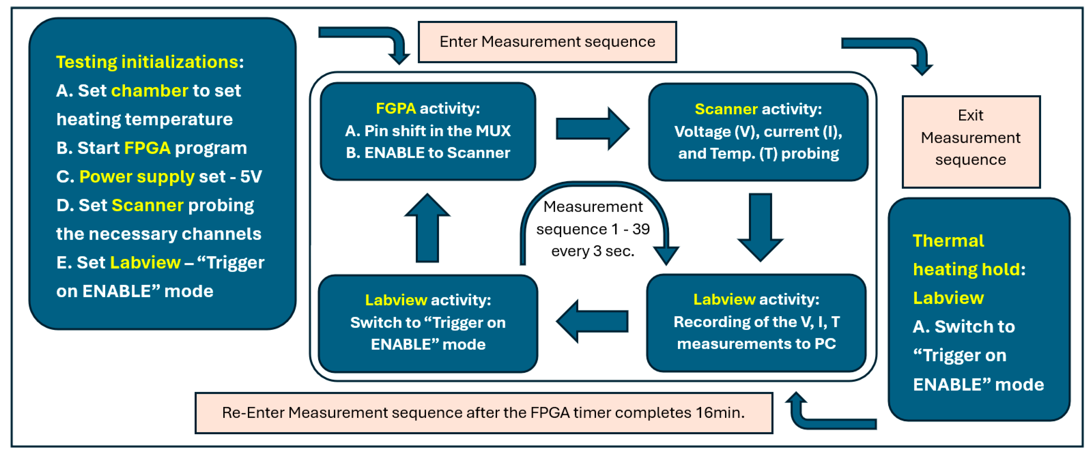
The timing sequence of the whole system is detailed in Figure 2. The sequence can be divided into three distinct phases:
  • Steps to initialize the system.
  • The measurement sequence.
  • System operation between sequences.
At the start of the test, several initial steps are performed. Manual tasks include preparing the thermal chamber by setting the temperature to the ambient testing point. The M300 Scanner DMM channels at configured to probe the voltage current and temperature. The power supply is initialized with DC output voltage of 5 V. The FPGA program must be manually programmed at the start of the test.
Following the initialization process, the automated testing procedure begins with the Labview program polling for an ENABLE signal from the FPGA. The FPGA raises an ENABLE flag which causes the system to transition into the pin measurement sequence mode. The Labview program is considered the “conductor” of the measurements. Labview receives a trigger signal from the FPGA indicating that the MUX in the FPGA is incrementing through one of the 39 pins to the next pin in the sequence. Simultaneously, the FPGA send an ENABLE signal to the Scanner. The program senses that the flag is raised and records data from the M300 for temperature, voltage, and current. It then returns to trigger on ENABLE mode. Each pin remains open for 3 s. This allows ample time for the Scanner to perform accurate measurements. In total, the sequence duration is 3 × 39 = 117 s.
After the sequence is completed, the system exits the measurement sequence and enters the thermal hold mode. It will stay in this mode until the FPGA clock completes a total of 16 min. Ultimately, the FPGA clock is the timing reference for the whole system.
The stress used for the testing suite of this study was fixed high temperatures. The logic behind this choice is that the object of the inspection is to portray stress conditions that are commonly seen in the field. This serves to set the foundation for a real-time monitor of the system’s I/O nets. The duration of the tests ranged from 200 to 300 h. The test cases and results are details in the next section.

3. Experimental

3.1. High Temperature Testing Results

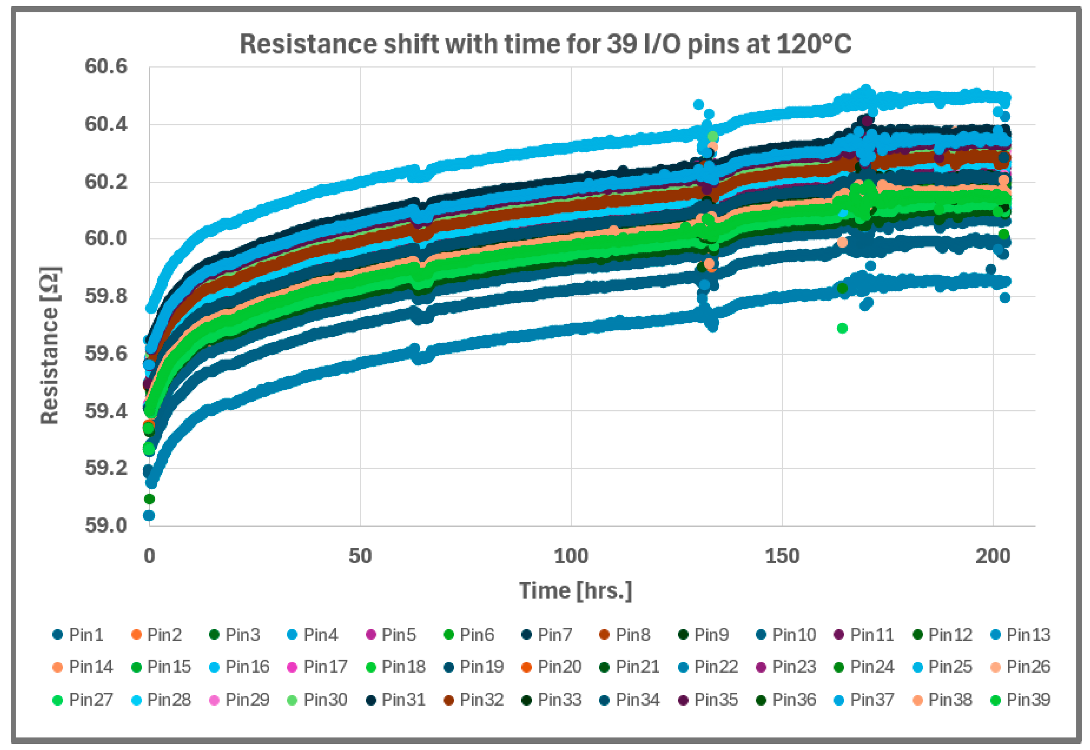
Four high temperature experiments were performed to formulate a degradation trend for different temperatures. The outcome of the testing generates a base for development of a real-time I/O net monitor because it demonstrates the sensitivity of the monitor to follow changes in the devices based solely on increased temperature. The temperatures chosen were as follows: 120 °C, 110 °C, 100 °C, and 80 °C. These temperatures are all within operation conditions possible for on-field devices, which have temperature limits of 125 °C. Although many studies chose to base degradation trends for packaging assemblies on thermal cycling stress, the stress performed in this study was deliberately chosen to be fixed high temperatures to follow degradation trends in the pass gate transistors. Thermal cycle can cause a recovery effect while fixed high temperature will show in situ testing results. The testing of the system showed notable results. Figure 3 is a plot of the resistance to time for 39 I/O nets which ran for the duration of about 200 h at an ambient temperature of 120 °C. Initial resistance is about 60 Ω for all nets. The resistance is calculated from the voltage difference in the inspection board and the voltage reading on the resistor as represented in Equation (1):
R I / O = V V i / R 250
The plot attests to the increase in resistance that follows a distinct power law.

3.2. Estimating the N-Root Power Law to Calculate the TTF

To formulate an I/O net monitor, it is critical to obtain an expected lifetime database. This is used to gauge resistance changes in the monitor to assess the health of the I/O nets. The lab-tested data is evaluated to create a profile of expected failure times that will serve as the control data set. As mentioned in the previous section, the data trend in each degradation plot shows an increase in resistance that follows a time law. The task at hand is to find the law that best fits the data set to show the aging with time. The data is transformed into a plot with the x-axis as the time to the n-root power. Figure 4 is a summation of the four temperatures tested showing a single I/O net per temperature and plotting the curves to the n-root transformed axis which is explained later in this section. The result is a plot that resembles a linear increase in resistance. It is clearly visible in the plots in Figure 4 that slope increases with the temperature increase. Also, the sensitivity of the resistance readings to temperature difference is shown by the offset of the plots by the different temperatures. A failure criterion of 10% increase is chosen for system. Figure 5 portrays the extrapolation of the data to a resistance value of 110%, which is the TTF. Equations (2) and (3) give the expression for TTF in hours:
ϑ = s l o p e R f : R 0 / t f 1 n : t 0 1 n
where R f : R 0 is the range of resistance values and t f 1 n : t 0 1 n is the range of time values converted to a n-root axis.
T T F 0.1 = 0.1 ϑ n
It should be noted that the expression is raised to the power of n to convert the time of the TTF to hours.
There are numerous approaches for realizing the n-root power of data, both analytically and empirically. One common method for measuring the n-root law is by plotting the data with the log of time in the x-axis and degradation variable (in our case resistance) also in the log scale over the initial point. This method was not chosen for this work because of two major problems. Firstly, it is virtually impossible to measure an initial point. Even small deviations in the initial point will cause major changes to the n-root value. The procedure used in this work was to start by plotting the data to a log–log scale. In the case the data does not degrade with the log of time, the plot will have an upwards curvature. The curvature is canceled by solving with a second order polynomial fit. Further details including an expanded explanation about this methodology will be revealed in an additional study. The fit calculation was conducted on all the I/O net data curves separately.
Figure 6 shows a histogram of the n-root values found for the resistance shift data of the 120 °C test. Similar results were received for the other tests. The results show a tight distribution of values centered at an n-value with a mean of 2.64. Additionally, the following statistical qualities are as follows:
  • Standard deviation (SD): ≈0.1019
  • 95% Confidence Interval (CI) for the mean: (2.6050, 2.6710)
  • t-test (H0: mean = 0):
    t-statistic: ≈ 161.72
    p-value: ≈ 0
Considering the figures above, the data is very tightly clustered. The variation in the results is justified due to noise in the data of the different pin plots. The value was chosen to find the TTF estimations of all the data curves.
As mentioned above, the plots are transformed into TTF estimations using a time law fit and extrapolating to 10% increase in I/O net resistance. This failure criterion is chosen because the 10% resistance increase has significant ramifications on the I/O performance. The procedure for estimating TTF values mentioned above was used to calculate the failure times for all the plots in the four test scenarios. Weibull distribution plots were figured for the data set. The procedure for plotting the Weibull distributions was conducted using ExcelTM formulas. Equation (4) is used to plot the Weibull distribution:
l n ln 1 I / O   p a t h #   = β l n ( T T F )
where I / O   p a t h # is the number of I/O nets in each test. The 39 I/O nets in our case. β is the shape parameter of the Weibull distribution. This value provides information about the level of determinability of the results.
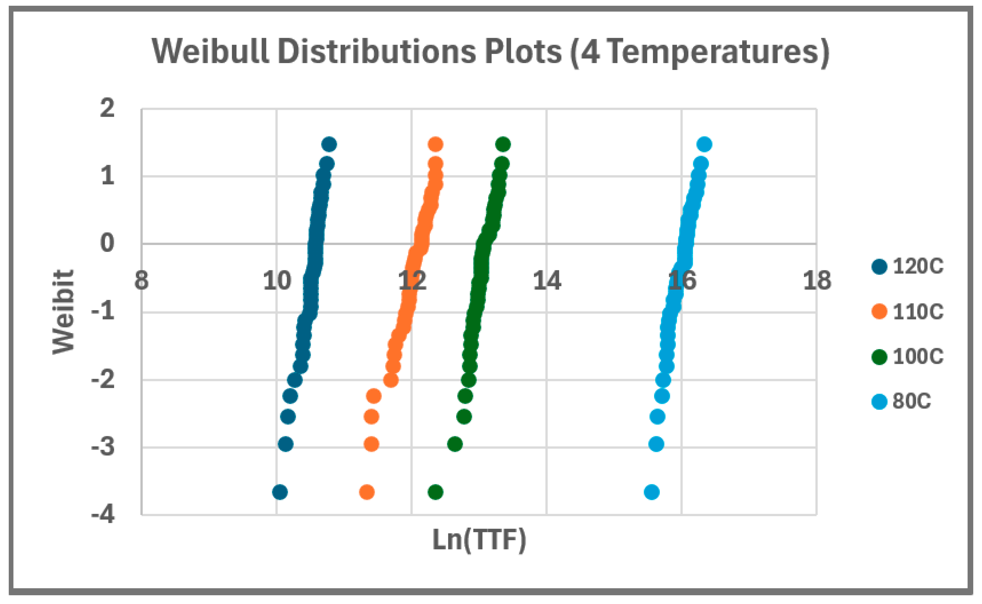
Figure 7 shows the Weibull distributions of all the tests. The β values range from about 4 to 7. The statistical significance of the results is a topic of investigation. In any case, these numbers are consistent with packaging tests. Table 1 lists the n-root values, the average TTF values per test, and the β parameter for the tests in all the temperatures.
The data shows a degradation trend with a decrease in TTF with the increase in ambient temperature. The next step is to find a fitting model to explain the data. Thermal stress is causing the change in degradation. Therefore, a simple Arrhenius model is used as is displayed in Equation (5):
T T F T S   = A 0 e x p E A , T S k T
Figure 8 displays the analysis of the mean TTF (MTTF) values using the model in Equation (4). The analysis shows an activation energy of 0.62 eV. This sheds light on revealing the dominant mechanism that causes degradation to the I/O net. This strengthens the theory that the prominent shift in the net is due to VTH shift in the transistor pass gate. It seems that the high temperature and voltage stress on the pass gate is causing bias temperature instability in the pass gate. The activation energy of 0.62 eV is close to characteristic activation energy of BTI, which is within the range of 0.5–0.56 eV. In summary, there are three strong proofs that BTI is the chief cause for resistance degradation in the set of tests. The first is that the stress conditions of constant high temperatures are effective at causing a substantial shift in resistance while solder pins and interconnects are less prone to large changes in constant high temperatures. Secondly, the EA is consistent with BTI degradation. Finally, the resistance changes greatly exceed what can be tolerated for tracking crack growth in bonds or electromigration in interconnects. In any case, further investigations must be made to verify the relative impact of all degradation causes. This study is underway.

4. Packaging Spatial Profiles

We have demonstrated how the test system successfully detects a degradation trend at high temperatures. An added dimension to the inspection is received by profiling the degradation trends according to the location of the I/O nets on the package. Figure 9 displays the relative degradation of each I/O net in the form of heat maps. The relative degradation is defined as the local TTF value normalized by the highest TTF value of the test. A major advantage received by implementing spatial monitoring is the ability to reveal local “hot spots” on the package where there are consistent short TTF times. In these results the bottom-right side of the monitored pins has consistently low TTF times. This can be due to the location of the I/O pins located close to the corner for the chip. The pins may be more vulnerable to concentrated heat stress and therefore lead to bond crack growth [21]. Beyond the region, the spatial inspection shows a comparatively high level of unpredictability. Although the current orientation is limited to less than 25% of the area of the chip, the location of the pins in a similar monitoring system can be optimized to cover a larger area in the chip.

5. Real-Time I/O Interconnection Net Monitor

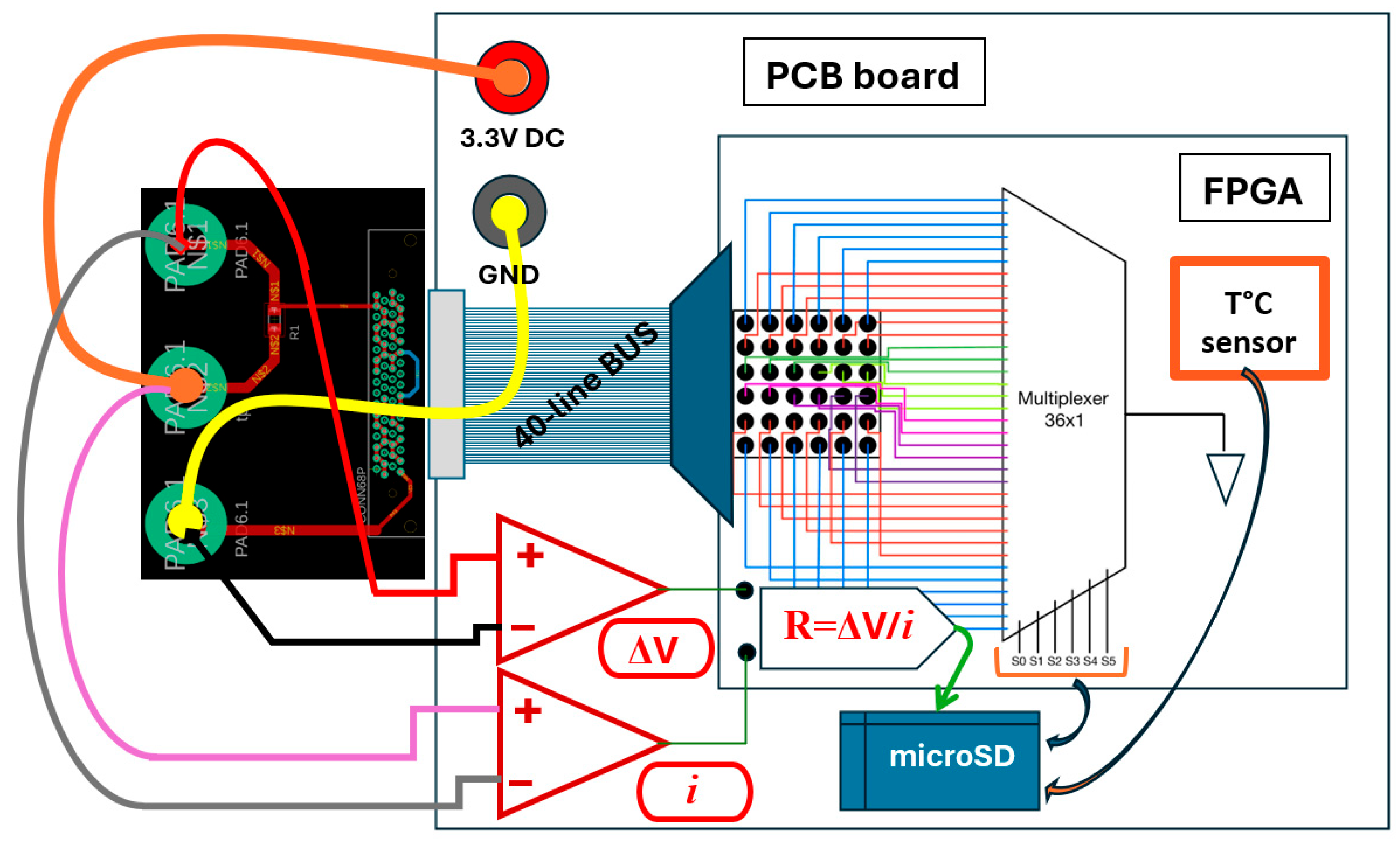
The previous sections of this work demonstrated the abilities of the I/O net testing procedure to follow degradation trends that provide rich diagnostic information about single package elements. Section 4 showed how the system can sense TTF vulnerabilities that are location-specific in the I/O nets. The results of the degradation tests establish a trend of resistance shift that is dependent on the ambient temperature. The remaining task is to modify the monitoring system to be applicable to devices in the field. Figure 10 shows a diagram of a proposed real-time monitor of I/O nets that can be implemented into an FPGA board with minimal resource expenses and additional space. The FPGA is programed with the 39-input MUX (in a DMUX orientation). The board will have an additional two ADC chips to calculate the current and voltage. There is also a thermal sensor to monitor the ambient temperature. Ambient temperature is the stressor to compare the real-time TTF reading to a bank of expected TTF estimates. The alarm criterion is 10% TTF readings compared to the TTF database values.
In Figure 9, we demonstrated the application of a spatial monitor of the system tested. The same concept can be applied similarly for the implementation of spatial monitors in most common packages. The procedure for automating location-based early fault warnings is conducted using a translation of the mapped pins (stored in the pin-out file of the FPGA) to their location on the chip. This information can be translated to indicate the placement of each pin relative to the center of the chip and stored in the chip’s memory.
Figure 11 shows the diagram of the pin package of the tested FPGA (Spartan-6). The 39 monitored pins are marked with numbers showing their place in the sequence of the monitoring procedure. In this study, the suggested reference point is the center of the chip. This reduces calculations to indicate hotspots. The explanation for this is that outer pins have more vulnerabilities due to their distance from the center of the chip making them more prone to CTE stresses. This is also demonstrated in the heat maps in Figure 9. Therefore, a pin closer to the center of the chip that shows a short TTF would point to an unexpected design defect. In Table 2, the first few rows of the translation markers are listed. The pins are first categorized by their quadrant. Then, they are categorized by their x and y coordinates in respect to the chips center. The numbering is given for the pins by their placement in the sequence. The TTF values are calculated using Equations (1)–(3) in Section 3. Since data in the system is minimal, the FPGA memory bank is sufficient. Long-term data collection is accomplished using a microSD extension.
Figure 9 includes the use of the commentary inspection board with feedback connections to the ADCs on the board. This element can be easily minimized to a miniature card that will serve the same function. The outstanding advantage of the monitor proposed is that it is adaptable to a wide range of FPGA and ASIC devices with similar packaging technology. In turn, many of the concepts proposed in this study can be used to develop monitoring systems in more advanced orientations including through silicon vias (TSVs), CU pillars, etc.

6. Conclusions and Deductions

This work demonstrates spatial monitoring of numerous I/O nets in a flip-chip + FPGA package. The results from controlled-environment testing show a clear trend for a resistance increase due to high temperatures even in relatively mild stress conditions. Test results on 39 I/O nets in four temperatures show a dominant degradation pattern that is strongly influenced by BTI aging. This can be explained due to the voltage and temperature stress contribution on the large PMOS pass gate for each I/O net. BGA inputs also contribute to the degradation, but the effect is small compared to resistance shift due to the interconnects and pass gates.
Results of spatial TTF predictions of the four temperatures are presented. All temperatures reveal degradation behavior non-location specific in majority of the monitored space. This removes concern of local vulnerabilities due to the design apart from the outer edge of the chip. The findings of this study will be complemented with failure analysis (FA) investigations such as scanning electron microscopes (SEM) and cross section images to fortify the conclusions in an additional study.
The experimental findings facilitate the erection of a novel spatial monitoring system capable of monitoring I/O nets over the area of the chip. The design and implementation of the monitor is proposed to allow I/O net self-monitoring using only the resources of a standard FPGA and a simple pin monitor circuit. The concept requires no external power or monitoring equipment.

Author Contributions

Conceptualization, E.B.; methodology, E.B.; validation, M.S.; formal analysis, M.G.; investigation, E.B.; resources, T.A.; data curation, T.A.; writing—original draft preparation, E.B.; writing—review and editing, E.B.; visualization, E.B.; supervision, M.G.; project administration, M.S.; funding acquisition, M.G. All authors have read and agreed to the published version of the manuscript.

Funding

This research received no external funding.

Institutional Review Board Statement

Not applicable.

Informed Consent Statement

Not applicable.

Data Availability Statement

Data are contained within the article.

Acknowledgments

Many thanks for the ongoing support from Ariel University Advanced Studies Research Group, Ariel, Israel.

Conflicts of Interest

The authors declare no conflict of interest.

References

  1. Alghassi, A.; Perinpanayagam, S.; Samie, M.; Sreenuch, T. Computationally Efficient, Real-Time, and Embeddable Prognostic Techniques for Power Electronics. IEEE Trans. Power Electron. 2015, 30, 2623–2634. [Google Scholar] [CrossRef]
  2. Ahsan, M.; Stoyanov, S.; Bailey, C. Prognostics of Automotive Electronics with Data Driven Approach: A Review. In Proceedings of the 39th International Spring Seminar on Electronics Technology (ISSE), Pilsen, Czech Republic, 18–22 May 2016; pp. 279–284. [Google Scholar] [CrossRef]
  3. Johnson, D.M. Review of fault management techniques used in safety-critical avionic systems. Prog. Aerosp. Sci. 1996, 32, 415–431. [Google Scholar] [CrossRef]
  4. Vichare, N.; Pecht, M. Prognostics and Health Management of Electronics. IEEE Trans. Compon. Packag. Technol. 2006, 29, 222–229. [Google Scholar] [CrossRef]
  5. Louen, C.; Ding, S.X.; Kandler, C. A new framework for remaining useful life estimation using support vector machine classifier. In Proceedings of the Control Fault-Tolerant Systems Conference, Nice, France, 9–11 October 2013; pp. 228–233. [Google Scholar] [CrossRef]
  6. Bender, E.; Bernstein, J.B. Microchip Health Monitoring System Using the FLL Circuit. Sensors 2021, 21, 2285. [Google Scholar] [CrossRef]
  7. Ghoshal, A.; Prosser, W.H.; Kim, H.S.; Chattopadhyay, A.; Copeland, B. Development of embedded piezoelectric acoustic sensor array architecture. Microelectron. Reliab. 2010, 50, 857–863. [Google Scholar] [CrossRef]
  8. Habib, F.; Martinez, M.; Artemev, A.; Brothers, M. Structural health monitoring of bonded composite repairs—A critical comparison between ultrasonic Lamb wave approach and surface mounted crack sensor approach. Compos. Part B Eng. 2013, 47, 26–34. [Google Scholar] [CrossRef]
  9. Lall, P.; Islam, N.; Suhling, J. Prognostication and health monitoring of leaded and lead free electronic and MEMS packages in harsh environments. In Proceedings of the 55th IEEE Electronic Components and Technology Conference (ECTC), Orlando, FL, USA, 1–3 June 2005; pp. 1305–1313. [Google Scholar] [CrossRef]
  10. Byttner, S.; Rögnvaldsson, T.; Svensson, M. Consensus Self-organized Models for Fault Detection (COSMO). Eng. Appl. Artif. Intell. 2011, 24, 833–839. [Google Scholar] [CrossRef]
  11. Bender, E.; Bernstein, J.B.; Boning, D.S. Modern Trends in Microelectronics Packaging Reliability Testing. Micromachines 2024, 15, 398. [Google Scholar] [CrossRef] [PubMed]
  12. Bhate, D.; Chan, D.; Subbarayan, G.; Chiu, T.C.; Gupta, V.; Edwards, D.R. Constitutive Behavior of Sn3.8Ag0.7Cu and Sn1.0Ag0.5Cu Alloys at Creep and Low Strain Rate Regimes. IEEE Trans. Compon. Packag. Technol. 2008, 31, 622–633. [Google Scholar] [CrossRef]
  13. Kumar, P.; Huang, Z.; Chavali, S.C.; Chan, D.K.; Dutta, I.; Subbarayan, G.; Gupta, V. Microstructurally Adaptive Model for Primary and Secondary Creep of Sn-Ag-Based Solders. IEEE Trans. Compon. Packag. Manuf. Technol. 2012, 2, 256–265. [Google Scholar] [CrossRef]
  14. Bernstein, J.B.; Bensoussan, A.; Bender, E. Reliability Prediction for Microelectronics, 1st ed.; Wiley Series in Quality & Reliability Engineering: Hoboken, NJ, USA, 2024; ISBN 978-1394210930. [Google Scholar]
  15. Ouyang, F.-Y.; Tu, K.; Lai, Y.-S. Effect of electromigration induced joule heating and strain on microstructural recrystallization in eutectic SnPb flip chip solder joints. Mater. Chem. Phys. 2012, 136, 210–218. [Google Scholar] [CrossRef]
  16. Dandu, P.; Fan, X.; Liu, Y.; Diao, C. Finite element modeling on electromigration of solder joints in wafer level packages. Microelectron. Reliab. 2010, 50, 547–555. [Google Scholar] [CrossRef]
  17. Clement, J.J.; Thompson, C.V. Modeling electromigration-induced stress evolution in confined metal lines. J. Appl. Phys. 1995, 78, 900–904. [Google Scholar] [CrossRef]
  18. Peng, J.; Huang, D.M.; Jiao, G.F.; Li, M.F. A Reliability Model for CMOS Circuit Based on Device Degradation. In Proceedings of the IEEE 11th International Conference on Solid-State and Integrated Circuit Technology, Xi’an, China, 29 October–1 November 2012; pp. 1–3. [Google Scholar] [CrossRef]
  19. Velamala, J.B.; Sutaria, K.B.; Ravi, V.S.; Cao, Y. Failure Analysis of Asymmetric Aging Under NBTI. IEEE Trans. Device Mater. Reliab. 2012, 13, 340–349. [Google Scholar] [CrossRef]
  20. Bernstein, J.B.; Bensoussan, A.; Bender, E. Reliability prediction with MTOL. Microelectron. Reliab. 2017, 68, 91–97. [Google Scholar] [CrossRef]
  21. Wu, X.; Yang, X.; Ye, J.; Liu, G. Novel Prognostics for IGBTs Using Wire-Bond Contact Degradation Model Considering On-Chip Temperature Distribution. IEEE Trans. Power Electron. 2025, 40, 4411–4424. [Google Scholar] [CrossRef]
Figure 1. The testing system of the device including stressing and monitoring instruments. The numbers label the different sections of the testing system. The numbers on the figure are detailed in the text.
Electronics 14 03549 g001
Figure 2. A sequence diagram of the testing system. Yellow font indicates test phases and instruments.
Electronics 14 03549 g002
Figure 3. Plot of 39 I/O nets showing the increase in resistance to time in an ambient temperature of 120 °C.
Electronics 14 03549 g003
Figure 4. Set of plots comparing the resistance shifts in the four different temperatures and showing the data on the converted n-root time law.
Electronics 14 03549 g004
Figure 5. The extrapolation of data to the I/O net failure criterion which is defined as a 10% increase in resistance. The broken red line represents the section of a data trend. The broken yellow line is the extrapolation beyond the data until reaching the point defined by the failure criterion.
Electronics 14 03549 g005
Figure 6. A histogram showing the statistical distribution of n-values using a binomial fit of all 39 I/O nets.
Electronics 14 03549 g006
Figure 7. Weibull distribution plots of the TTF values in all four temperatures.
Electronics 14 03549 g007
Figure 8. Average TTF values plotted to find the activation energy of the degradation mechanism.
Electronics 14 03549 g008
Figure 9. Heat maps (ad) giving a spatial perspective of the relative impact of resistance degradation on the I/O nets displayed in 80 °C, 100 °C, 110 °C, and 120 °C tests. Green represents relatively long TTF values and red represents relatively short failure times.
Electronics 14 03549 g009
Figure 10. Diagram of the proposed I/O path health solution ready to be implemented on a FPGA development board. The system utilizes all elements managed in the test system without the need of external instruments.
Electronics 14 03549 g010
Figure 11. Diagram of the package of the test FPGA. The numbered pins (in the non-shaded area are the monitored pins according to their sequence in the monitoring cycle. The package is sectioned into four quadrants marked with the broken orange lines and marked with numbers.
Electronics 14 03549 g011
Table 1. N-root values for the high temperature tests.
Test CaseN-RootTTF (Averaged) β Parameter
80 °C2.6938,626,033 h.5.933
100 °C2.748455,674 h.5.665
110 °C2.634162,387 h.4.196
120 °C2.63836,566 h.6.984
Table 2. I/O pins to package-pin quadrants transfer for spatial sensing.
Input#Quadrant#x-Distancey-Distance
0478
1468
2448
3423
Disclaimer/Publisher’s Note: The statements, opinions and data contained in all publications are solely those of the individual author(s) and contributor(s) and not of MDPI and/or the editor(s). MDPI and/or the editor(s) disclaim responsibility for any injury to people or property resulting from any ideas, methods, instructions or products referred to in the content.