Article

Bit Synchronization-Assisted Frequency Correction in Low-SNR Wireless Systems

1
School of Electronic Information and Electrical Engineering, Chengdu University, Chengdu 610106, China
2
Chengdu Zhongdian Jinjiang Information Industry Co., Ltd., Chengdu 610051, China
3
Chengdu Kinyea Technologies Co., Ltd., Chengdu 610097, China
*
Authors to whom correspondence should be addressed.
Electronics 2025, 14(12), 2319; https://doi.org/10.3390/electronics14122319
Submission received: 4 May 2025 / Revised: 1 June 2025 / Accepted: 4 June 2025 / Published: 6 June 2025
(This article belongs to the Section Microwave and Wireless Communications)

Abstract

In wireless communication systems, traditional frequency synchronization methods struggle to effectively track carrier frequency in low signal-to-noise ratio (SNR) environments, leading to degraded demodulation performance and severely impacting the stability and reliability of communication systems. To address this challenge, an innovative frequency synchronization framework is introduced, enhancing frequency synchronization accuracy and robustness in low-SNR environments through bit synchronization techniques. Specifically, the approach constructs a “bit synchronization-frequency synchronization” joint correction mechanism, where clock offset information extracted during the bit synchronization process is utilized to estimate frequency offset. This method enables an indirect measurement and compensation of carrier frequency offset, forming a hierarchical error compensation system. Furthermore, to overcome the limited convergence speed of the classical Gardner algorithm under significant phase offset conditions, an improved error feedback structure is proposed, accelerating bit synchronization convergence and reducing timing synchronization errors, thereby enhancing overall system performance. The effectiveness of the proposed method is validated through theoretical analysis and simulation experiments. Simulation results demonstrate that, compared to conventional frequency synchronization schemes, the proposed method achieves higher frequency correction accuracy in low-SNR scenarios, thereby improving the robustness and anti-interference capability of wireless communication systems in complex environments.

1. Introduction

In wireless communication systems, frequency synchronization is a critical process to ensure accurate signal demodulation and reliable data recovery. Particularly in low signal-to-noise ratio (SNR) environments, traditional frequency synchronization methods often suffer from insufficient precision, slow convergence, or even synchronization failure, severely affecting the stability of the communication link. Carrier frequency offset (CFO), a key factor that influences communication system performance, is typically caused by Doppler effects, hardware mismatches, or clock drift, leading to an increased bit error rate (BER) and degraded signal quality. Therefore, developing a frequency synchronization method suitable for low-SNR environments is of paramount importance.
Existing frequency synchronization methods can be broadly categorized into data-aided and non-data-aided algorithms. Data-aided synchronization algorithms, such as the Kay algorithm [1], L&W algorithm [2], and L&R algorithm [3], exhibit superior synchronization accuracy and acquisition speed under high-SNR conditions. However, these methods rely on pilot signals, which reduce transmission efficiency and make adaptation to complex channel environments challenging. In contrast, non-data-aided synchronization algorithms, such as frequency offset estimation using FFT [4,5], Costas loops [6,7], and decision-directed loops [8], do not require pilot signals and perform stably in high-SNR scenarios. However, in low-SNR environments, these methods are highly susceptible to noise interference, leading to increased frequency estimation errors and potential synchronization failures. To address these challenges, this paper proposes an improved bit synchronization-assisted frequency correction method that enhances synchronization accuracy and robustness in low-SNR conditions.
Furthermore, bit synchronization is a crucial technology in wireless communication systems [9,10,11,12] and faces its own set of challenges. For instance, frame synchronization algorithms relying on data-aided methods can introduce phase offsets under significant frequency deviations, exposing the limitations of error feedback mechanisms in bit synchronization, such as the Gardner algorithm. The slow feedback convergence of bit synchronization further restricts its direct application in frequency synchronization. Several optimization strategies have been proposed to address these issues, including improved interpolation filters [13], pre-filtering methods [14,15], and compensation techniques [16,17]. In [18], a hardware-based improved loop filter was designed to enhance transmission efficiency. However, these methods often suffer from high computational complexity or offer limited performance improvements. To fully exploit the potential of bit synchronization in frequency synchronization, this paper proposes a bit synchronization-assisted frequency correction method and introduces an enhanced Gardner algorithm to improve its convergence performance, ensuring synchronization accuracy and stability in low-SNR environments.
Specifically, this study extracts clock offset information between the transmitter and receiver during the bit synchronization process to indirectly estimate frequency offset. The estimated value is then used for frequency compensation before entering the conventional frequency synchronization stage, thereby alleviating the burden on Costas loops or phase-locked loops (PLLs). Additionally, to address the slow convergence of the Gardner algorithm under large frequency offsets, an improved algorithm is proposed, optimizing the error feedback mechanism to enhance convergence speed and stability.
The primary contributions of this paper are as follows. First, a bit synchronization-assisted frequency synchronization method is proposed, demonstrating superior noise resilience in low-SNR environments and significantly improving frequency synchronization accuracy. Second, the Gardner algorithm is enhanced to improve its convergence performance under large frequency offsets. Finally, a comprehensive theoretical analysis and algorithmic framework is established, thoroughly investigating the robustness and convergence properties of the proposed method.
This research not only presents a novel solution for frequency synchronization in low-SNR environments but also provides theoretical support and practical engineering value for the efficient synchronization design of future wireless communication systems. The remainder of this paper is structured as follows. Section 2 reviews the system model for bit synchronization, Section 3 and Section 4 describe the proposed frequency synchronization method and the improvements to the Gardner algorithm, respectively. Section 5 evaluates the proposed method through simulations and experimental results. Section 6 presents further discussion. Finally, conclusions are drawn in Section 7.

2. System Modeling

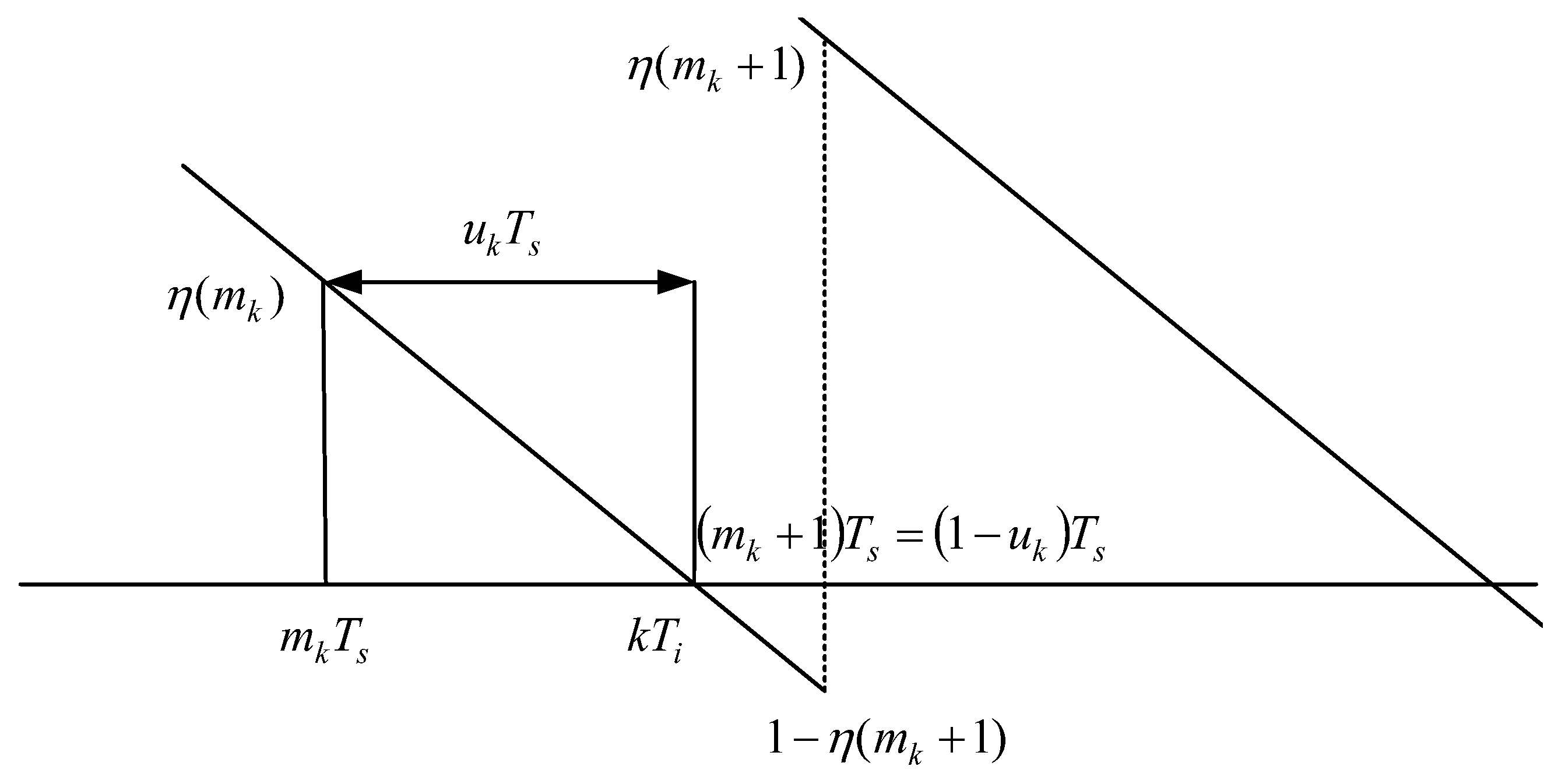
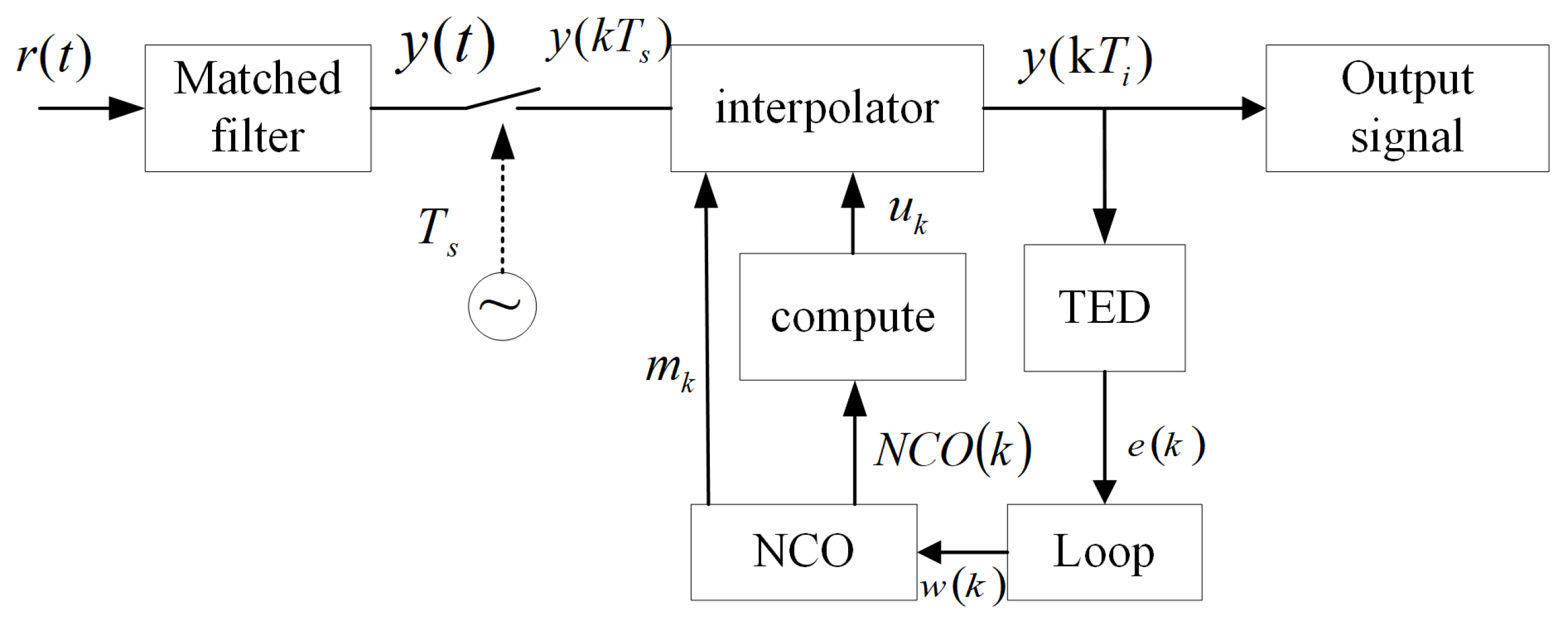
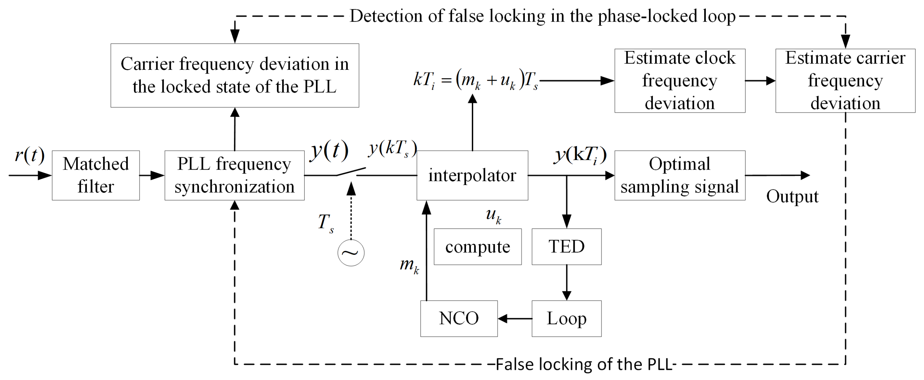
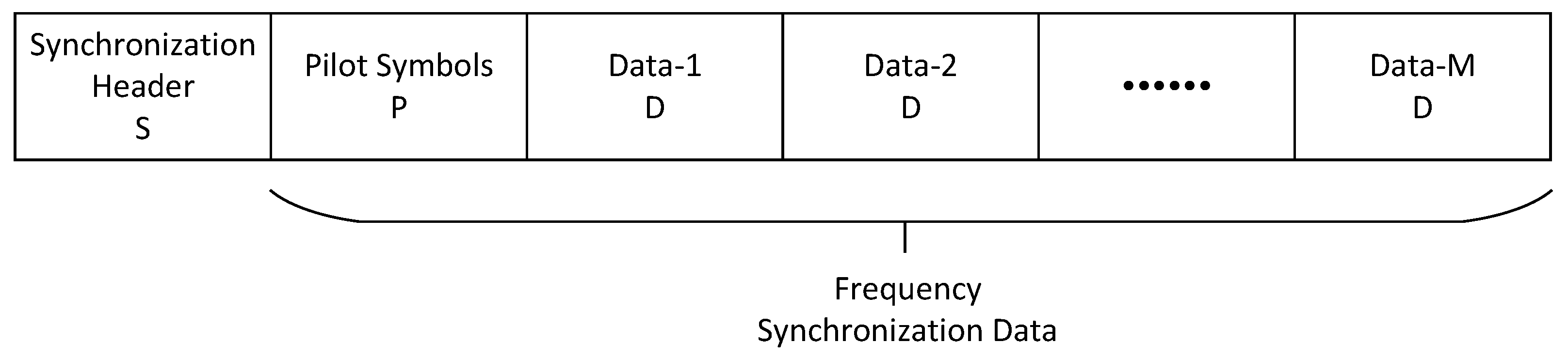
2.1. Timing Synchronization Feedback Model

Whether using a phase-locked loop (PLL)-based frequency synchronization method or a data-aided (DA) approach that employs training sequences for frequency estimation, the performance of these methods deteriorates significantly as the signal-to-noise ratio (SNR) decreases. In low-SNR environments, frequency estimation based on training sequences is highly susceptible to noise interference, leading to substantial estimation bias. Meanwhile, PLL-based frequency synchronization methods may suffer from false locking or an inability to track carrier frequency offset. Furthermore, under the same SNR and loop noise bandwidth conditions, timing synchronization loops generally exhibit stronger noise resistance than frequency synchronization loops and can effectively correct bit synchronization deviations.
On the other hand, in wireless communication systems, carrier frequency offset is influenced not only by channel conditions and Doppler effects but also by the inherent oscillator inaccuracies of the transmitter and receiver devices [19]. Based on this observation, this paper extends the existing timing synchronization module to extract timing offset information and further compute the frequency offset, thereby achieving more accurate frequency synchronization. This method effectively improves frequency synchronization accuracy in low-SNR environments and improves system robustness.
After downconversion, the received BPSK/QPSK signal is first passed through a matched filter and then sampled according to the local sampling frequency f s = 1 / T s . The sampled signal is then fed into the timing recovery loop. The output signal of the matched filter can be expressed as follows:
y ( t ) = n y ( n T ) h ( t n T τ n ) + n ( t )
where y ( n T ) represents the received symbol sequence, h ( t ) is the impulse response of the matched filter, and n ( t ) denotes additive noise. T is the symbol period, and n is the index of the transmitted symbols. τ n represents the timing offset caused by the mismatch between the receiver and transmitter sampling periods. By sampling the matched filter output signal y ( t ) at intervals of m T s (where m = 0, 1, 2, …), the second sampling value at t = m T s can be expressed as
y ( t ) = m y ( m T s ) h ( t m T s τ s ) + n ( m T s )
where T s is the clock period of the receiver’s fixed sampling rate, T is the symbol period, and τ s represents the timing delay caused by the discrepancy between the receiver’s local sampling clock period and the transmitter’s sampling period.
To compensate for synchronization deviations caused by timing delays, time synchronization is required for signals sampled at the local sampling clock frequency f s . This process is achieved through a time synchronization module.
The time synchronization module is a closed-loop system comprising an interpolation filter, a timing error detector, a loop filter, and a numerically controlled oscillator (NCO). Specifically, the interpolation filter employs a polyphase decomposition interpolation algorithm based on the Farrow structure. It generates interpolation coefficients through polynomial fitting and performs fractional interval resampling on the input signal.
In the timing synchronization and bit synchronization module, the interpolation filter is used to perform fractional interval resampling on the signal y ( k T s ) , thereby recovering the signal values at the optimal sampling instants.
To generate the desired optimal interpolated signal, y ( t ) can be represented as a resampled signal at intervals of k T i (where k = 0, 1, 2, …). The interpolation at the kth instance, occurring at t = k T i , can be expressed as
y ( k T i ) = m y ( m T s ) h ( k T i m T s ) + n ( k T i )
After passing through the interpolation filter, the interpolation timing t k of the kth symbol can be expressed as t k = k T s τ s , where τ s represents the timing offset estimation of the kth symbol.
The timing error detector employs the Gardner algorithm. The classical Gardner algorithm calculates the timing error signal based on the error characteristics of adjacent I/Q symbol samples, with the error function expressed as
e ( k ) = e I ( k ) + e Q ( k ) = y I ( k 1 / 2 ) [ y I ( k ) y I ( k 1 ) ] + y Q ( k 1 / 2 ) [ y Q ( k ) y Q ( k 1 ) ]
where y I ( k ) and y Q ( k ) denote the resampled in-phase (I) and quadrature (Q) components of the k-th symbol, respectively. The terms e I ( k ) and e Q ( k ) represent the timing errors in the I and Q branches. y I ( k ) and y I ( k 1 ) correspond to the optimal sampling points of the I branch, while y I ( k 1 / 2 ) represents the intermediate sample between two optimal sampling points. The value of y I ( k 1 / 2 ) is proportional to the timing error in the I branch, while y I ( k ) y I ( k 1 ) determines the timing error adjustment direction. The same principles apply to the Q branch.
The loop filter is responsible for smoothing e ( k ) and filtering out noise, which determines the loop stability and the time required to establish synchronization. In this work, an ideal integrating loop filter is utilized to effectively track the phase and frequency offset between the local clock and the transmitted symbol clock. The output of the loop filter controls the numerically controlled oscillator (NCO) through the control word w ( m ) , which can be expressed as
f p = C 1 e ( k )
w ( m + 1 ) = w ( m ) + C 2 e ( k ) + f p
In the bit synchronization module, the NCO is responsible for generating clock overflow events, which determine the interpolation reference point m k and simultaneously compute the fractional interval u k for interpolation.
η ( m + 1 ) = [ η ( m ) w ( m ) ] m o d 1
where η ( m ) represents the content of the NCO register at the m-th clock cycle, and w ( m ) is the NCO control word, both of which are positive fractional values. Since the NCO operates at a cycle of T s , while the interpolator operates at a cycle of T i , the loop filter adjusts w ( m ) to ensure that the NCO overflows precisely at the optimal sampling instants. When the loop reaches equilibrium, w ( m ) approximately stabilizes to a constant value. At this point, the NCO register overflows once every 1 / w ( m ) cycles of T s , on average. Therefore, the interpolation period is given by
T i = T s / w ( m )
which leads to
w ( m ) = T s / T i
The variation of the NCO register content over time is illustrated in the following figure.
In Figure 1, m k T s represents the sampling clock pulse point, which precedes the k-th interpolation instant k T i , This interpolation instant corresponds to the zero-crossing point of the curve, marking the overflow moment of the numerically controlled oscillator (NCO). The recursive relationship governing interpolation control can be derived by expressing two consecutive interpolation instants as follows:
k T i = ( m k + u k ) T s
( k + 1 ) T i = ( m k + 1 + u k + 1 ) T s
where m k and m k + 1 are integers. Subtracting these two equations yields the recursive formula
m k + 1 = m k + T i / T s + u k u k + 1
From Figure 1, by applying the principle of similar triangles, the following relationship is obtained:
u k η ( m k ) = 1 u k T s 1 η ( m k + 1 )
Thus, the fractional interval can be expressed as
u k = η ( m k ) w ( m k )
Once the interpolation basepoint m k and the fractional interval u k are determined, the bit synchronization feedback system utilizes these values to compute the correct interpolation point. The corresponding clock timing error is then calculated based on the interpolation point. This error is processed by the loop filter to update the step size w ( m ) , which is subsequently fed into the controller to compute m k and u k . The entire system continuously adjusts through feedback to determine the optimal interpolation point, thereby outputting the best sampling data.The feedback system is illustrated in Figure 2.

2.2. Common Source Characteristics of Sampling and Carrier Clocks

In wireless communication systems, the sampling clock f s t x _ c l k and carrier clock f c t x _ c l k are derived from a common reference clock f r e f through phase-locked loop (PLL) frequency multiplication, ensuring signal synchronization and coherence. Their mathematical relationship is expressed as
f s t x _ c l k = N s f r e f f c t x _ c l k = N c f r e f
where N s and N c represent the frequency multiplication factors for the sampling and carrier clocks, respectively. Ideally, both f s t x _ c l k and f c t x _ c l k are determined solely by f r e f and their respective multiplication factors. However, in practical systems, non-ideal PLL characteristics introduce frequency deviations, primarily due to the following factors.

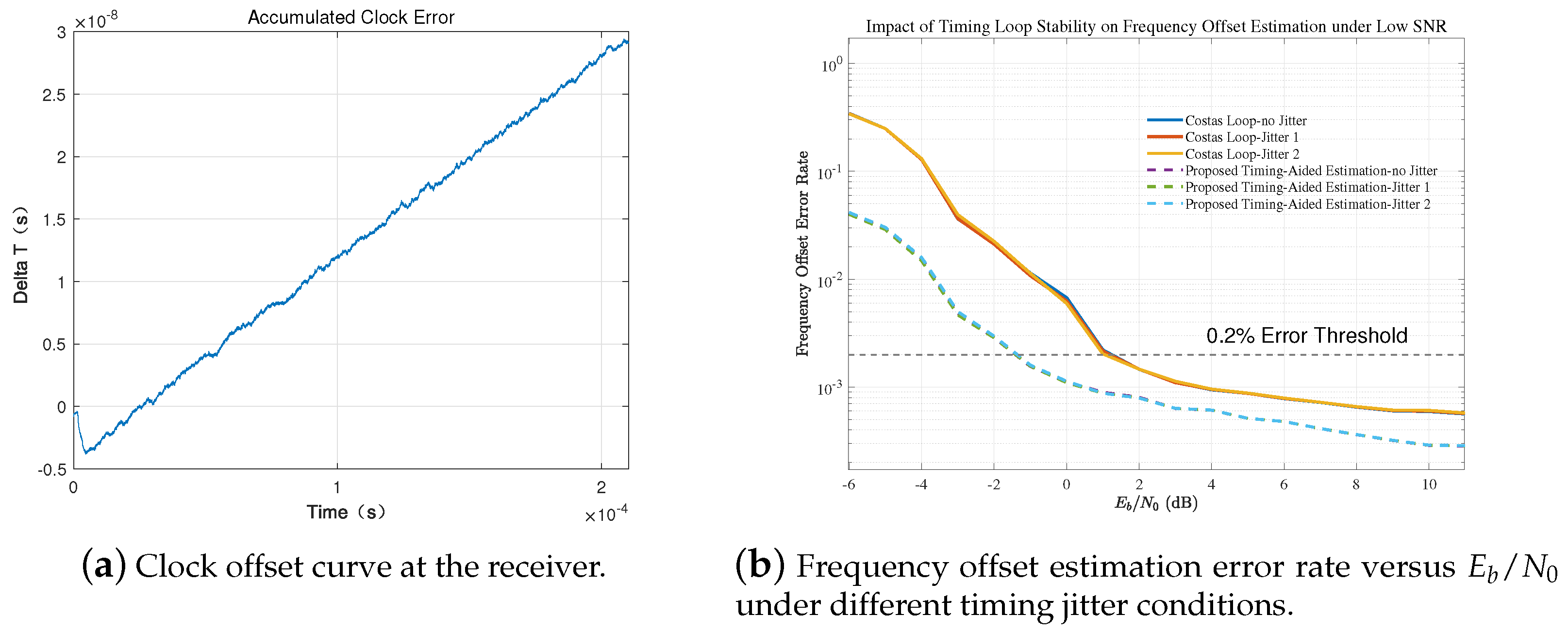
2.2.1. Reference Clock Drift

Due to temperature variations, component aging, and other environmental factors, the actual reference clock frequency deviates by Δ f r e f , leading to shifts in the multiplied clock frequencies:
f s t x _ c l k = N s ( f r e f + Δ f r e f ) = f s t x _ c l k + N s Δ f r e f f c t x _ c l k = N c ( f r e f + Δ f r e f ) = f c t x _ c l k + N c Δ f r e f
When N s N c , the minor deviation Δ f r e f is amplified by the multiplication factors, resulting in an accumulated frequency error between the sampling and carrier clocks, which adversely affects synchronization performance.

2.2.2. Relative Offset Between Sampling and Carrier Clocks

In practical implementations, the PLLs at the transmitter and receiver may have different loop parameters, such as loop bandwidth B L and gain K, leading to inconsistencies in their output clock signals. If the transmitter and receiver PLLs introduce additional frequency Δ f P L L , the estimated carrier frequency offset Δ f c and sampling clock offset Δ f c l k at the receiver can be expressed as
Δ f c l k = f s t x _ c l k f s t x _ c l k = N s Δ f r e f + Δ f P L L
Δ f c = f c t x _ c l k f c t x _ c l k = N c Δ f r e f + Δ f P L L
Since both clocks originate from the same reference frequency, their offsets are related by
Δ f c = N c N s Δ f c l k
Thus, when the PLL multiplication factors differ ( N s N c ), the sampling clock frequency deviation is proportionally mapped to the carrier frequency deviation by a factor of N c N s , affecting subsequent carrier synchronization and demodulation accuracy.
In summary, the sampling and carrier clocks are both derived from the reference clock f r e f via PLL frequency multiplication, with their deviations primarily influenced by reference clock drift, PLL errors, and noise accumulation effects. When the multiplication factors differ, minor reference clock deviations are magnified, leading to increased frequency errors at the receiver, necessitating compensation via synchronization modules.

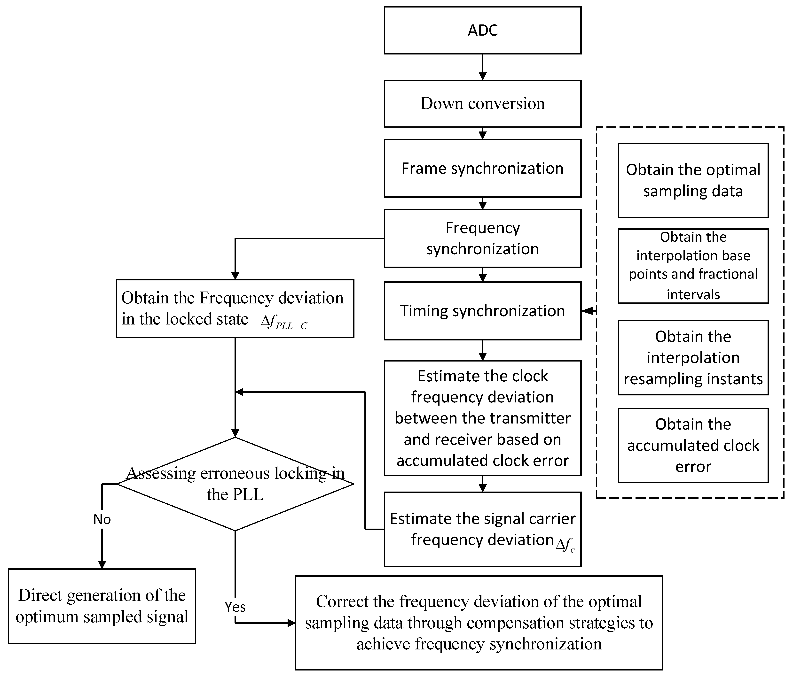
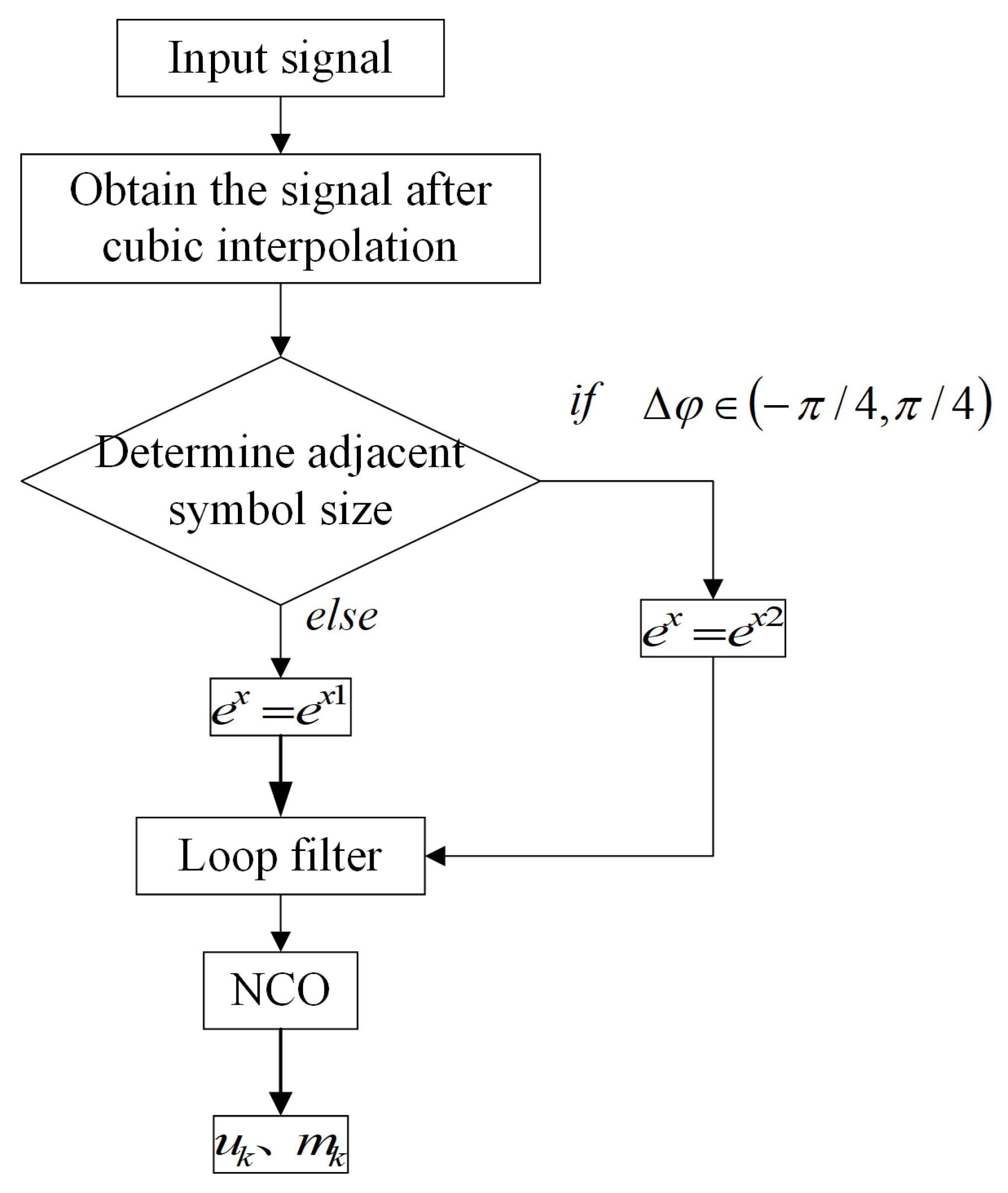
3. Carrier Frequency Offset Estimation

To track the frequency offset caused by clock drift, the receiver utilizes a Gardner-based timing recovery loop to estimate symbol timing offset. The key system parameters are defined as follows:
  • sample : Receiver upsampling factor;
  • N c : Ratio of carrier frequency to sampling clock frequency ( N c = f c tx _ clk / f s tx _ clk );
  • N s : Ratio of symbol rate to sampling rate ( N s = f s tx _ clk / R s where R s is symbol rate).
As the accumulated timing error over multiple frames reflects the underlying clock offset between the transmitter and receiver, the linear trend (slope) of this timing drift is extracted. This estimated drift slope is then mapped to a coarse frequency offset, which is used for pre-compensation prior to fine carrier synchronization using a phase-locked loop (PLL). A loop filter is employed to smooth the clock offset estimation, ensuring robustness to noise while maintaining sensitivity to time-varying drift.
During the bit synchronization process, the optimal sampling point data is obtained, along with key interpolation parameters. The interpolation parameters are defined as
  • m k : Interpolation basepoint index (integer part of timing offset);
  • u k : Fractional interval ( 0 u k < 1 );
  • k T i : Ideal symbol-spaced sampling instant where k is the symbol index.
In the clock synchronization process based on the Gardner algorithm, the timing error detector (TED) requires two samples per symbol. Therefore, during the bit synchronization stage, the original signal y m T s is downsampled using a stride index m e = (0, 2, 4, …) that selects every second sample, corresponding to sampling instants:
t = m e T s
In practical scenarios, sampling clock offsets exist between the transmitter and receiver, causing the receiver’s sampling instants to gradually drift away from the optimal sampling points. To quantify this deviation, the accumulated clock error Δ T a c c u ( k ) between receiver samples and ideal symbol instants is defined as
Δ T a c c u ( k ) = m e T s k T i
k T i = ( m k + u k ) T s
where m e T s represents the sampling instant of the received signal when two samples per symbol are taken based on the receiver’s clock, while k T i denotes the interpolation instant generated by the bit synchronization module. The accumulated clock error Δ T a c c u ( k ) captures the cumulative effect of clock drift between the transmitter and receiver.
To analyze the temporal evolution of this accumulated error, two reference indices ( N 1 and N 2 , where N 2 > N 1 ) and a time window N w i n d o w . At these two reference indices, the mean accumulated clock error is computed as follows:
Δ T l o c k = m e a n ( Δ T a c c u ( N 2 : N 2 + N w i n d o w ) ) m e a n ( Δ T a c c u ( N 1 : N 1 + N w i n d o w ) )
where m e a n ( ) represents the averaging operation over multiple measurements to mitigate noise and enhance estimation accuracy. The actual time interval between the two reference indices is given by
Δ t l o c k = ( N 2 N 1 ) T s
From the accumulated clock error difference Δ T l o c k and the actual time interval t l o c k , the clock drift rate can be estimated as
R d r i f t = Δ T l o c k / Δ t l o c k
This parameter quantifies the rate of clock offset between the transmitter and receiver. Given the receiver’s upsampling factor s a m p l e and the sampling clock period T s , the clock frequency offset between the transmitter and receiver can be calculated as
Δ f c l k = R d r i f t / ( T s s a m p l e )
where Δ f c l k denotes the relative clock frequency offset between the transmitter and receiver.
In wireless communication systems, the carrier frequency f c t x _ c l k is derived from the transmitter’s clock f s t x _ c l k . Thus, clock frequency offset induces a corresponding carrier frequency offset:
Δ f c = f c t x _ c l k Δ f c l k f s t x _ c l k N c N s Δ f c l k
where Δ f c represents the carrier frequency offset caused specifically by the clock frequency offset. This equation highlights that even small discrepancies in the transmitter and receiver clocks can be significantly amplified at high carrier frequencies, thereby increasing carrier frequency error.
To ensure robust carrier synchronization, the lock state of the phase-locked loop (PLL) is evaluated based on the relative motion between the transmitter and receiver. Let Δ f PLL _ c denote the PLL’s estimated frequency offset after convergence. In typical terrestrial mobile communication scenarios, Doppler-induced frequency shifts generally range from 0 Hz to approximately 1000 Hz. If the absolute difference between these two values, | Δ f PLL _ c Δ f c | , exceeds 1000 Hz, the system declares a carrier synchronization failure, as this deviation is unlikely to result from normal Doppler variation and more likely indicates tracking loss or acquisition error.
Upon detecting carrier synchronization failure, a secondary frequency compensation process is performed to achieve frequency alignment. The compensation strategy involves the following:
  • Coarse Frequency Correction—The optimal sampled data undergoes frequency offset compensation using a digital down-conversion approach to obtain a coarsely corrected signal;
  • Fine Frequency Correction via PLL—The coarse frequency-compensated signal is further refined using a PLL, which tracks and adjusts the residual frequency error;
  • Phase Ambiguity Resolution—The fine frequency-compensated signal is further processed to resolve phase ambiguity, thereby completing the frequency synchronization process.
This approach ensures accurate carrier synchronization, mitigating the impact of clock-induced frequency errors in wireless communication systems.The flowchart of the proposed frequency synchronization method is shown in Figure 3, and the detailed framework is illustrated in Figure 4.

4. Modified Timing Synchronization Loop

In the classical Gardner algorithm (denoted as the GA algorithm), if the adjacent sampled symbols y ( k ) and y ( k 1 ) exhibit the same polarity, the intermediate sampling value y ( k 1 2 ) may deviate from zero, even when the timing error has been corrected. This deviation introduces system self-noise, adversely affecting the accuracy of timing error estimation and thereby degrading synchronization performance.
To enhance clock error detection and timing recovery, countermeasures must be implemented when adjacent symbol polarities are identical to mitigate the impact of system self-noise.
Compared to the GA algorithm, an improved method proposed in [17], referred to as the mGA1 algorithm, inverts e I ( k ) and e Q ( k ) when adjacent symbol polarities in the I or Q channels are identical. However, its bit error rate (BER) performance in a high-bandwidth wireless communication link model remains comparable to that of the GA algorithm.
Building on this, an extended non-data-aided detector, denoted as the mGA2 algorithm, was introduced in [20]. This method demonstrates superior timing jitter performance over the mGA1 detector under ideal phase recovery conditions. Nevertheless, when carrier frequency offset is present, the mGA2 algorithm can introduce greater timing noise errors, increasing the risk of bit synchronization failure.
Additionally, an enhanced Gardner algorithm with self-noise suppression capabilities, referred to as the mGA3 algorithm, was proposed in [21]. This method significantly outperforms other improved Gardner algorithms in terms of timing noise error reduction. However, its synchronization speed is relatively slow.
Addressing these challenges, this study integrates the strengths of various improved Gardner algorithms and proposes an optimized detection method based on phase compensation and complex signal joint decision-making. This approach aims to reduce timing jitter, accelerate synchronization convergence, and minimize timing noise errors.

4.1. Self-Noise Suppression in Error Detection

Based on the mGA3 algorithm, self-noise in the error detection mechanism is reduced. The error function is expressed as
e m G A 3 k = e I m G A 3 k + e Q m G A 3 k
Expanding this yields
e m G A 3 ( k ) = y I k 1 2 h ( T 2 ) h ( 0 ) y I ( k ) + y I ( k 1 ) × y I ( k ) y I ( k 1 ) + y Q k 1 2 h ( T 2 ) h ( 0 ) y Q ( k ) + y Q ( k 1 ) × y Q ( k ) y Q ( k 1 )
The term h T 2 h 0 = 2 cos ( α π / 2 ) π ( 1 α 2 ) , where α represents the roll-off factor of the pulse shaping filter h ( t ) .

4.2. Optimization of the Error Function

Building upon the error function, a new optimized error function is defined as
e x 1 ( k ) = e I ( m G A 3 ) ( k ) + e Q ( m G A 3 ) ( k )
e I ( m G A 3 ) ( k ) = e I x ( k ) , if sign y I ( k ) sign y I ( k 1 ) e x ( k ) , else e Q ( m G A 3 ) ( k ) = e Q x ( k ) , if sign y Q ( k ) sign y Q ( k 1 ) e Q x ( k ) , else
where s i g n ( ) extracts the sign of the signal.
Further considering the phase difference between adjacent symbols Δ φ , when Δ φ [ π / 4 , π / 4 ) , a new error term is defined as
e x 2 ( k ) = α R e ( | e j a r g ( y ( k ) ) e j a r g ( y ( k 1 ) ) | c o n j y k 1 2 )
where α is the roll-off factor, R e ( ) denotes the real part, and c o n j ( ) represents complex conjugation.

4.3. Final Expression of the mGA4 Algorithm

The final error detection mechanism of the mGA4 algorithm is formulated as
e x ( k ) = e x 1 ( k ) , if Δ φ π 4 , π 4 e x 2 ( k ) , if Δ φ π 4 , π 4
This method integrates the convergence speed of the mGA2 algorithm with the self-noise suppression capability of the mGA3 algorithm. By incorporating phase compensation and complex signal joint decision-making, the approach effectively enhances timing jitter performance, accelerates synchronization convergence, and reduces timing noise errors. As a result, it significantly improves synchronization performance in wireless communication systems.The flowchart of the proposed mGA4 algorithm is illustrated in Figure 5.

5. Simulation Results

To evaluate the proposed algorithm, a wireless communication link model was established for simulation analysis. The transmitted signal frame structure consists of a preamble, pilot symbols, and data symbols. The preamble, comprising 139 symbols, is constructed using a Zadoff–Chu (ZC) sequence to achieve frame synchronization. The pilot segment, consisting of 460 symbols, is modulated using binary phase-shift keying (BPSK) and serves to resolve phase ambiguities introduced by the carrier synchronization phase-locked loop. The data section spans 100,000 symbols and is modulated using quadrature phase-shift keying (QPSK). The baseband signal at the transmitter has a symbol rate of 30.72 MHz, with an upsampling factor of 8, resulting in a sampling clock frequency of 245.76 MHz. A root-raised cosine (RRC) filter is employed for pulse shaping, with a roll-off factor of α = 0.5 . The system incorporates a clock frequency offset of 20 ppm. Considering the trade-off between computational complexity and interpolation accuracy, a cubic Lagrange interpolation filter is adopted for signal resampling.The overall baseband frame structure used in the simulation is illustrated in Figure 6.

5.1. Carrier Phase Noise and Jitter Modeling

To evaluate the robustness of the proposed synchronization algorithm under practical hardware impairments, we introduce phase jitter modeled from realistic local oscillator (LO) phase noise spectra. The phase noise is generated in the frequency domain according to a specified single-sideband (SSB) phase noise mask in dBc/Hz and converted into time-domain phase fluctuations through inverse Fourier transformation. The resulting complex-valued jitter signal is applied as a multiplicative term to the transmitted carrier as follows:
s jitter [ n ] = e j ϕ [ n ] ,
where ϕ [ n ] denotes the random phase sequence determined by the oscillator’s phase noise power spectral density.
The phase noise profiles used for jitter modeling were derived from a combination of ADIsimPLL simulations and empirical measurements of representative oscillator hardware, ensuring that the simulated jitter scenarios realistically capture practical operating conditions.
Two distinct jitter scenarios are simulated:
  • Jitter1: Represents a typical high-performance oscillator (e.g., HMC830 PLL with 875 MHz output), with phase noise values:
    L ( f ) = { 0 , 115 , 115 , 110 , 120 , 147 , 162 , 165 , 165 } dBc / Hz ,
    at frequency offsets f = { 0 , 10 2 , 10 3 , 10 4 , 10 5 , 10 6 , 10 7 , 10 8 , f s / 2 } Hz;
  • Jitter2: Models a degraded oscillator, increasing the phase noise at all frequency offsets by approximately 10 dB compared to Jitter1, thus representing a more severe jitter condition.
The root-mean-square (RMS) phase jitter in radians is calculated by integrating the phase noise power spectrum:
σ ϕ = 2 i = 2 k Δ f i · 10 L ( f i ) / 10 ,
where L ( f i ) is the phase noise power at offset f i , and Δ f i denotes the bin width in the discrete frequency domain.
The resulting RMS jitter values and normalized phase jitter percentage (relative to 2 π ) are summarized in Table 1.

5.2. Verification of Carrier Synchronization Performance

As shown in Figure 7a, the accumulated clock offset Δ T a c c u ( k ) results from sampling clock deviations between the transmitter and receiver. This offset is measured after applying the bit synchronization feedback algorithm combined with a Farrow-structure interpolation filter. The interpolation filter, controlled by the timing error feedback, iteratively compensates for timing deviations, enabling rapid convergence and thus ensuring precise sampling alignment, which is critical for bit synchronization.

Statistical Analysis

All error metrics were computed from N = 100 independent Monte Carlo trials. The 95% confidence intervals (CIs) were calculated using Student’s t-distribution with a significance level of α = 0.05 . Significant performance differences between methods were inferred from non-overlapping CIs.
Figure 7b illustrates the impact of timing loop stability on frequency offset estimation accuracy under various SNR and jitter conditions. When E b / N 0 falls below approximately −2 dB, the timing synchronization loop continues to converge; however, the accuracy of the timing estimates degrades due to increased noise, leading to bias and instability in the frequency offset estimation. In this regime, both the Costas-based and the proposed timing-aided methods exhibit estimation errors exceeding the 0.2% threshold. Nevertheless, the proposed method maintains significantly lower error rates and more stable performance compared to the Costas loop, which suffers from sharp degradation and pronounced sensitivity to jitter. These results indicate that the proposed approach remains more robust and reliable under extremely low-SNR conditions, demonstrating strong resilience to both noise and timing jitter.
Table 2 provides a comparative analysis of frequency offset estimation errors under various E b / N 0 conditions for the conventional Costas loop and the proposed algorithm. To emulate practical wireless impairments, multiplicative jitter is introduced in the carrier signal generated by the transmitter’s PLL, with two distinct jitter scenarios (Jitter1 and Jitter2) evaluated to assess algorithm robustness and stability.
Results demonstrate that the proposed algorithm consistently outperforms the Costas loop, particularly in low-SNR regimes, achieving significantly lower estimation errors. Furthermore, both methods maintain stable estimation performance across the jitter conditions, indicating that phase jitter exerts only a minor influence on their accuracy.
Overall, these findings confirm the superior accuracy and robustness of the proposed approach under challenging SNR conditions. While jitter has a limited impact on both algorithms, the proposed method delivers clear performance advantages, making it well-suited for deployment in complex wireless communication systems requiring high-precision frequency synchronization.

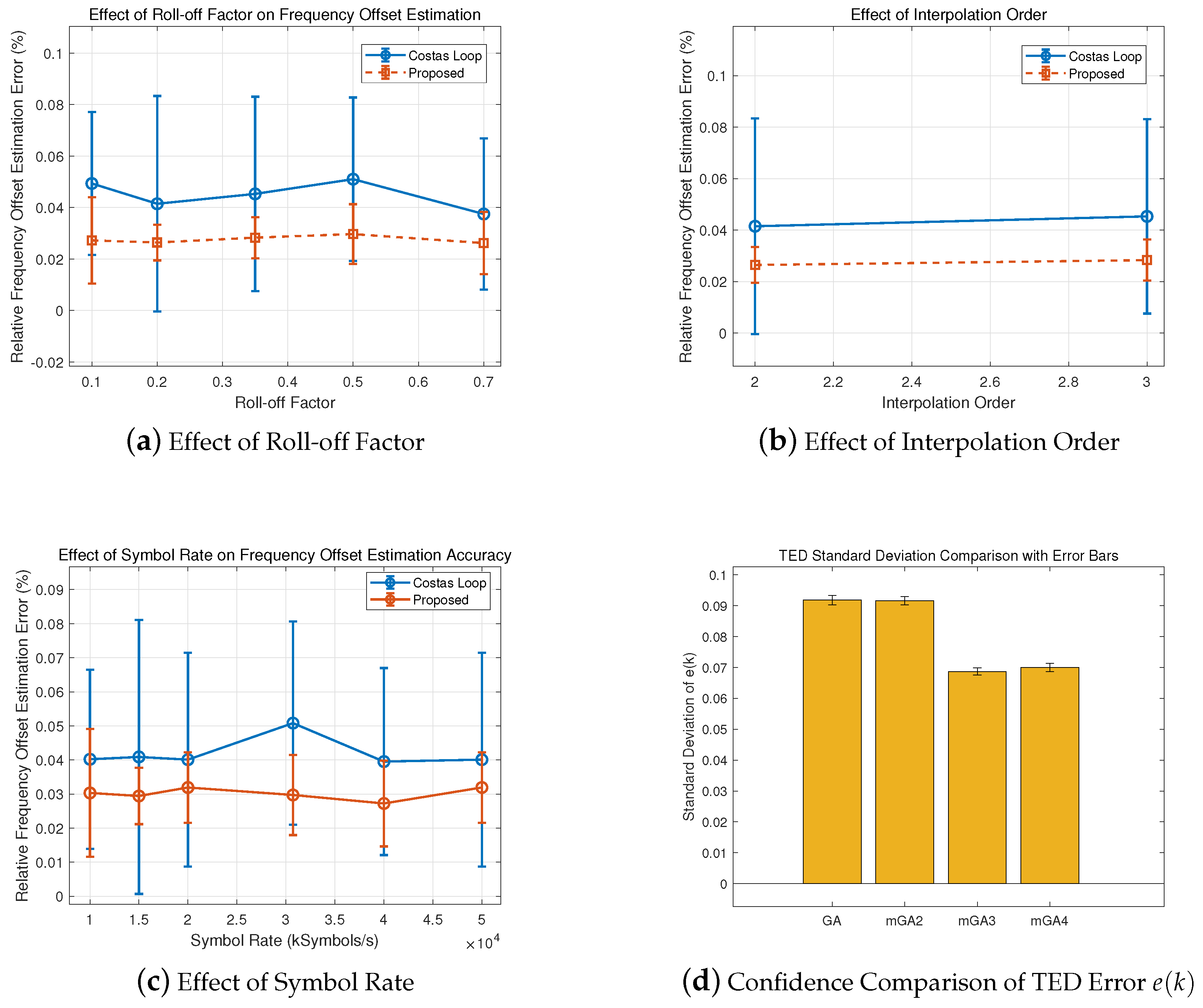
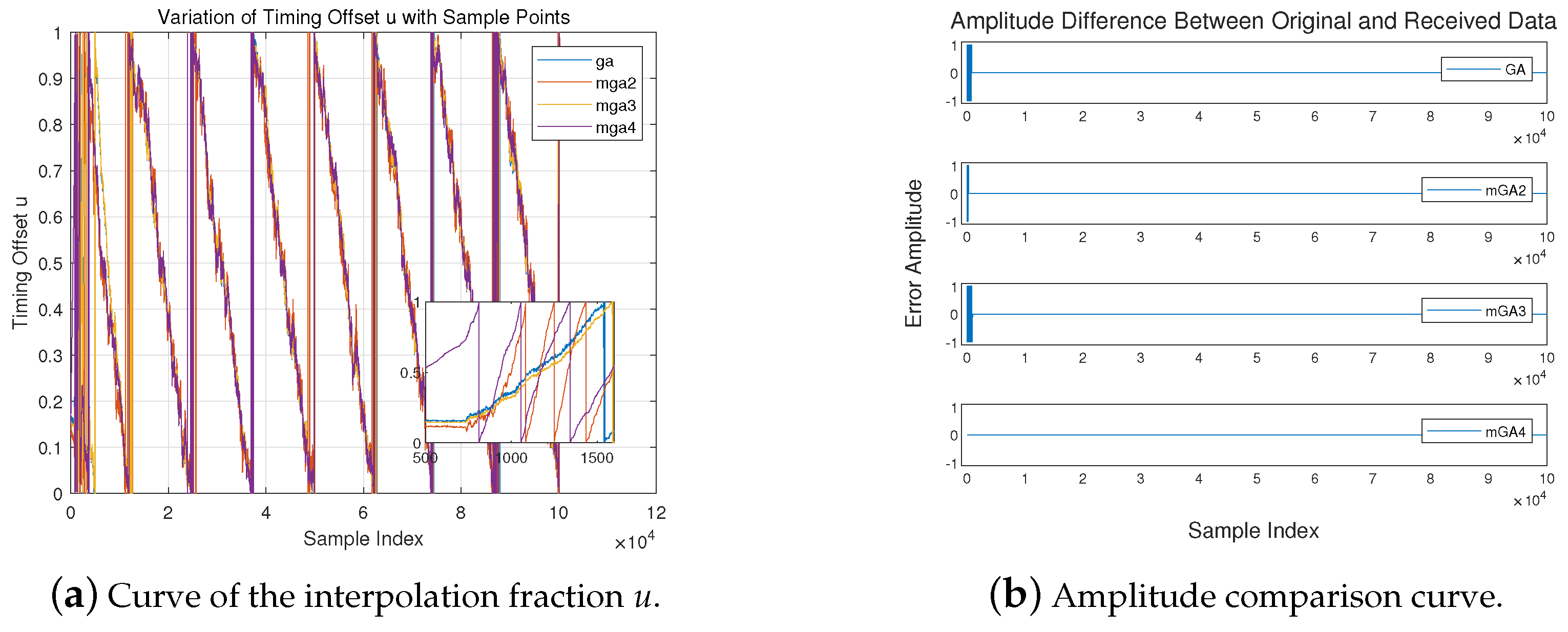
5.3. Validation of the Improved Timing Recovery Algorithm Performance

Under specific simulation settings, the convergence behavior of the fractional interval u k and timing error e ( k ) was analyzed to evaluate synchronization performance. Each algorithm was assessed over 100 independent runs, and Table 3 reports the standard deviation of the TED outputs.
At E b / N 0 = 12 dB, the proposed method ( e m G A 4 ( k ) ) achieved a standard deviation of 0.0700 ± 0.0013 , notably lower than that of the conventional Gardner algorithm ( 0.0918 ± 0.0015 ). For comparison, e m G A 2 ( k ) and e m G A 3 ( k ) yielded 0.0916 ± 0.0014 and 0.0687 ± 0.0012 , respectively.
Figure 8 further illustrates the influence of roll-off factor, interpolation filter order, and symbol rate on frequency offset estimation (subfigures a−c), and compares TED performance (subfigure d). All results are averaged over 100 trials, with error bars denoting standard deviations and 95% confidence intervals.
Figure 9 illustrates two key performance aspects of the proposed timing recovery algorithm. Subfigure (a) shows the evolution of the NCO output u k , where the mGA4 algorithm achieves significantly faster convergence compared to baseline methods, requiring fewer symbols to reach synchronization. This accelerated convergence shortens the acquisition period and improves overall timing stability. Subfigure (b) further validates the practical impact by comparing the received signal amplitude after bit synchronization correction under conditions of frame synchronization offsets and insufficient pilot symbols due to large frequency deviations. While GA, mGA2, and mGA3 exhibit initial bit errors—even under high SNR—mGA4 rapidly converges and maintains a zero bit error rate, demonstrating superior robustness and synchronization reliability under challenging conditions.

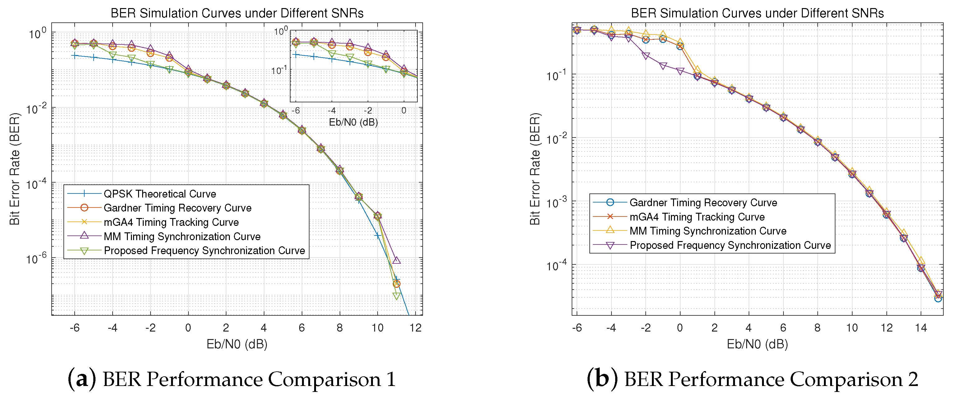
5.4. Evaluation of System Reliability and Efficiency

To ensure a fair and accurate performance evaluation of the communication system, the bit error rate (BER) and packet error rate (PER) were calculated exclusively over the data symbol segment, explicitly excluding both the preamble and pilot sections. Since the pilot symbols are used for synchronization and phase ambiguity resolution rather than conveying actual payload data, including them in BER/PER statistics would bias the results and overestimate system performance. Specifically, the BER (high SNR, initial 10 k) metric reflects the error rate over the first 10,000 data symbols, while BER (high SNR, full 500 k) represents the error rate over the entire 500,000-symbol data section.
To provide a more comprehensive system-level evaluation beyond synchronization performance, we further analyzed three key metrics: bit error rate (BER), packet error rate (PER), and data throughput. These system-level metrics provide insight into the actual reliability and efficiency of the communication link under each timing recovery scheme, beyond the synchronization layer.
As summarized in Table 4, the proposed mGA4 algorithm achieves the lowest BER and PER values across both short-term and long-term transmissions. Specifically, mGA4 attains a BER below 10 6 over 500k payload bits and a PER of only 0.6%, outperforming all baseline algorithms. Furthermore, due to its faster convergence (within 102 symbols), mGA4 enables earlier data recovery and achieves the highest effective throughput of 61.44 Mbps. These results demonstrate that improving synchronization accuracy not only stabilizes symbol timing but also significantly enhances overall system robustness and spectral efficiency.
In addition, the “Timing Convergence Symbols” metric quantifies the number of symbols required for the timing recovery loop to reach steady-state convergence after frame detection. A smaller value indicates faster synchronization and reduced vulnerability during the symbol acquisition phase. For instance, the proposed mGA4 algorithm achieves convergence within 102 symbols, significantly improving the timing recovery responsiveness and enhancing the overall robustness of the communication system.
To further validate system robustness under practical conditions, the BER performance was quantitatively evaluated across various SNR levels and synchronization scenarios. As illustrated in Figure 10, the proposed mGA4 algorithm consistently outperforms GA, mGA2, and mGA3 in terms of BER, particularly in the presence of frame synchronization offsets and limited pilot symbols. These improvements are attributed to faster timing convergence, which effectively reduces the vulnerability window during the initial phase of symbol recovery.

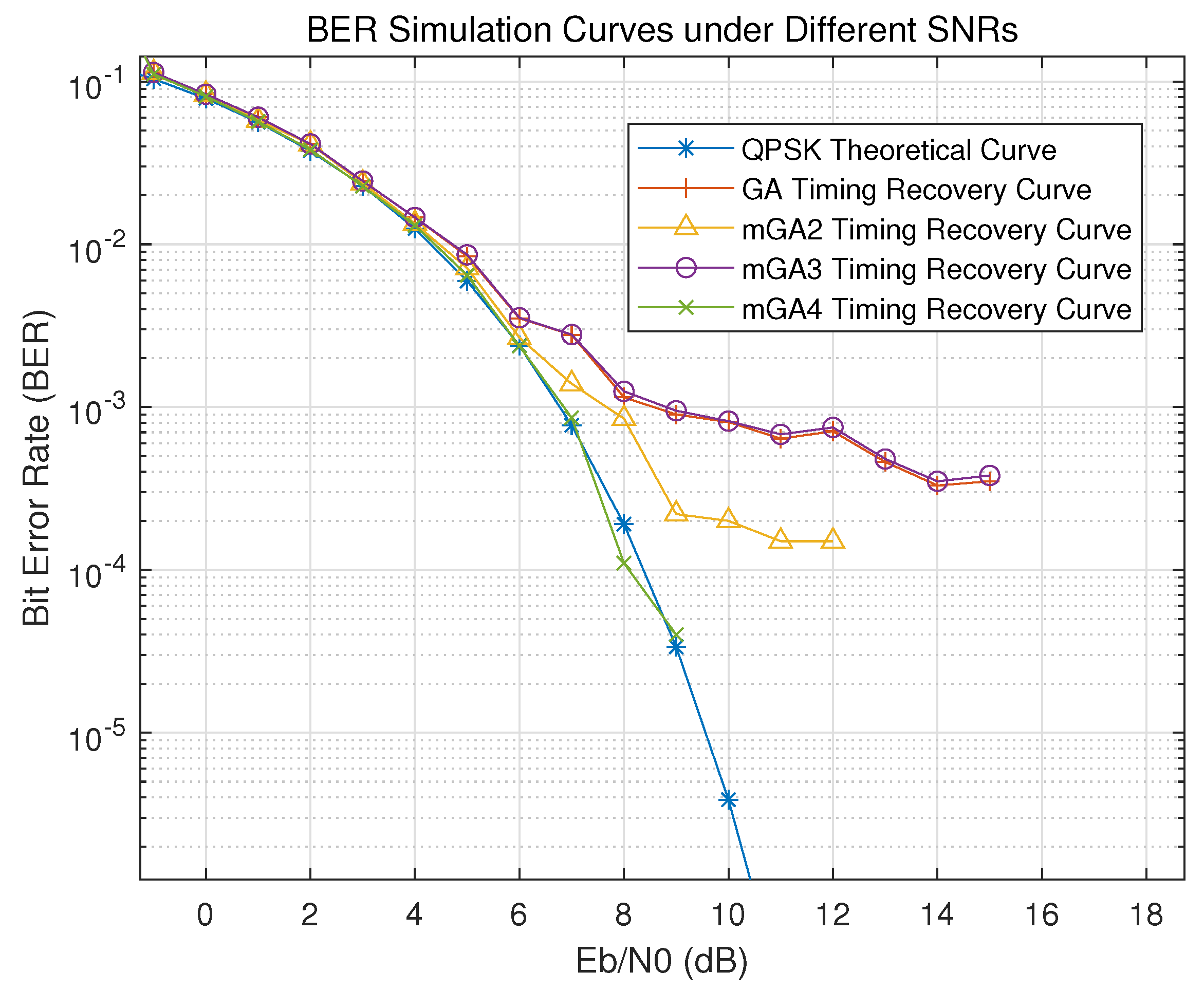
5.5. Bit Error Rate Optimization

By integrating the proposed optimization algorithm, the system achieves a bit error rate (BER) that closely aligns with the optimal theoretical error curve, even under low signal-to-noise ratio (SNR) conditions. Compared to the non-optimized system, the BER performance improves by approximately 2 to 3 orders of magnitude, as illustrated in Figure 11a.
To further evaluate the effectiveness of the proposed mGA4 algorithm in realistic mobile communication scenarios, additional simulations incorporated multipath fading and Doppler effects, which are representative impairments in outdoor wireless environments involving user mobility, such as urban or suburban mobile terminals.
The multipath fading channel was modeled with four distinct propagation paths, having relative delays of [0, 110, 190, 410] ns and corresponding power levels of [0, −9.7, −19.2, −22.8] dB, simulating signal reflections from nearby buildings and terrain. To emulate user movement at moderate speeds (e.g., 30–60 km/h), Doppler shifts were applied to the multipath components, resulting in time-varying frequency offsets at the receiver. This setup realistically reflects the dynamic channel behavior experienced in typical mobile wireless environments, such as vehicular communications or handheld devices in motion.
The results, presented in Figure 11b, demonstrate that the mGA4 algorithm maintains reliable performance under these challenging conditions. Despite inter-symbol interference (ISI) and time-selective fading, the proposed method achieves stable timing error convergence and yields a significantly lower BER compared to the classical Gardner algorithm. These findings confirm the robustness and suitability of mGA4 for mobile communication systems operating in dynamic, multipath-rich environments.

5.6. Computational Complexity Analysis

To evaluate the implementation feasibility of the proposed modified Gardner algorithm with polarity-based gating (mGA4) and two-layer drift correction, we analyze the computational complexity per received symbol and per frame.
The mGA4 algorithm extends the classical Gardner detector by introducing a gating mechanism based on polarity checks. This includes the computation of sign functions and XOR logic to suppress ineffective timing updates. The operations per symbol are constant and summarized as follows:
  • 4 sign evaluations (2 for in-phase and 2 for quadrature components);
  • 2 XOR logical operations;
  • 1 conditional timing error update.
A phase-based decision strategy is employed to improve timing accuracy. For each of the M candidate interpolated symbols (typically M = 4 ), the phase difference is computed and an error energy metric is evaluated. This involves the following:
  • 2 subtractions (real and imaginary);
  • 2 multiplications (for squaring);
  • 1 addition (error accumulation);
  • 1 comparison (minimum error selection).
The interpolation module uses cubic Lagrange interpolation with fixed coefficients, leading to the following:
  • 6 multiplications;
  • 6 additions.
These values are per interpolated point, regardless of the actual signal values.
The second-layer drift correction is performed via a linear regression over a sliding window of fixed length N (e.g., N = 32 ). The complexity includes the following:
  • N multiplications;
  • 2 N additions;
  • 1 division.
All operations in the algorithm are fixed and do not grow with the length of the input sequence. The summary of operation counts and complexity is shown in Table 5.
As all modules perform a fixed number of operations per symbol or per frame, and no recursive or variable-size operations are involved, we conclude that the proposed enhancements introduce a small, constant overhead, making them feasible for real-time implementation on DSP and FPGA platforms, as are common in wireless receivers. Sign comparisons, conditional logic, phase computations, and slope estimations are well-suited for efficient digital logic mapping. Moreover, the fixed number of operations in cubic interpolation can be pipelined using MAC units on modern FPGA or SoC devices.
Given the consistent O ( 1 ) complexity per symbol and frame, real-time processing at high sampling rates is achievable. Therefore, the proposed scheme is both computationally efficient and practical for deployment in SDR-based receivers such as those using ADRV9009 or USRP platforms.
To bridge the gap between simulation and deployment, preliminary hardware resource estimations have also been conducted, suggesting that the proposed synchronization logic can fit within mid-scale FPGAs. Furthermore, future work will proceed in two phases: (1) HDL-level prototyping and timing simulation, and (2) over-the-air testing on ADRV9009/USRP SDR platforms under realistic low-SNR and fading conditions.

6. Discussion

While the Costas loop is adopted as the baseline for performance evaluation in this study, we acknowledge the existence of more advanced frequency synchronization methods, including the Moose estimator, Schmidl & Cox (S&C) algorithm, Kim’s frequency offset estimator, Kalman filter-based approaches, and maximum likelihood (ML)-based synchronization techniques.
Among these, the Moose, S&C, Kim, and ML-based estimators typically rely on long, known training sequences and often require extensive correlation or search operations. This reliance can significantly increase computational complexity and bandwidth overhead, limiting their practicality in continuous transmission scenarios or resource-constrained environments such as IoT or deep-space systems.
In contrast, the proposed bit synchronization-assisted frequency correction method does not require any additional training sequences, as it derives frequency offset information directly from the clock offset obtained during the timing recovery process. This makes our method lightweight and well-suited for low-SNR and real-time systems.
Moreover, our method is not mutually exclusive with model-based approaches such as Kalman filtering. On the contrary, it can serve as a coarse initial estimator that provides a reliable frequency offset estimate, which can be recursively refined by Kalman-based filters. This layered combination is expected to improve convergence speed and robustness, particularly in dynamically varying channels. This will be investigated in our future work.
The classical Gardner timing recovery algorithm, although originally designed for QPSK modulation, has been demonstrated to be extendable to higher-order modulation formats like 16QAM and 64QAM. Our improved Gardner algorithm similarly maintains this extensibility, enabling accurate timing offset estimation for a range of modulation schemes.
In addition to the timing synchronization, the proposed two-layer synchronization framework employs clock offset information derived from the improved Gardner algorithm to estimate frequency offset. This frequency offset estimation mechanism is inherently modulation-agnostic and thus can also be extended to higher-order modulation formats.
Nonetheless, higher-order constellations feature closer symbol spacing, making them more vulnerable to residual synchronization errors, particularly timing inaccuracies. Such vulnerabilities can cause performance degradation, especially under low-SNR conditions or multipath fading channels.
To overcome these challenges, future work will focus on further optimizing both the improved Gardner timing recovery and the frequency offset estimation mechanism. Potential enhancements include decision-directed synchronization schemes, adaptive loop filters, and error-correction-assisted synchronization strategies, aiming to maintain robust synchronization performance across a broad range of modulation formats.

7. Conclusions

This work proposes a bit synchronization-assisted frequency correction method tailored for low-SNR wireless communication scenarios. By estimating the frequency offset through clock drift information and applying coarse correction before PLL tracking, the approach enhances frequency synchronization accuracy while maintaining low complexity. Experimental results demonstrate reduced convergence time and improved BER performance compared to the traditional Costas loop.
The proposed scheme is well-suited for real-time deployment in software-defined radios and embedded platforms due to its constant per-symbol complexity and hardware-friendly operations. Future efforts will focus on extending this method to more complex modulation schemes and benchmarking against state-of-the-art synchronization algorithms to validate its broader applicability and performance advantages.

Author Contributions

Conceptualization, J.G. and P.Y.; methodology, J.G. and P.Y.; software, Y.Z.; validation, J.G., P.Y. and T.L.; formal analysis, S.C.; investigation, P.Y.; resources, Y.Z.; data curation, J.G.; writing—original draft preparation, J.G. and P.Y.; writing—review and editing, P.Y. and T.L.; visualization, S.C.; supervision, P.Y. and T.L.; project administration, T.L. and Z.L. All authors have read and agreed to the published version of the manuscript.

Funding

This work was financially supported by the Sichuan Time Frequency Synchronization System and Application Engineering Technology Research Center Open Project for 2024 (grant no. 2024SPKT04).

Institutional Review Board Statement

Not applicable.

Data Availability Statement

The data that support the findings of this study are available from the corresponding author upon reasonable request.

Conflicts of Interest

Author Yilin Zhang was employed by the company Chengdu Zhongdian Jinjiang Information Industry Co., Ltd. Author Tao Liu was employed by the company Chengdu Kinyea Technologies Co., Ltd. The remaining authors declare that the research was conducted in the absence of any commercial or financial relationships that could be construed as a potential conflict of interest.

References

  1. Kay, S. A fast and accurate single frequency estimator. IEEE Trans. Acoust. Speech Signal Process. 1989, 37, 1987–1990. [Google Scholar] [CrossRef]
  2. Lovell, B.C.; Williamson, R.C. The Statistical Performance of Some Instantaneous Frequency Estimators. IEEE Trans. Signal Process. 1992, 40, 1708–1723. [Google Scholar] [CrossRef]
  3. Luise, M.; Reggiannini, R. Carrier frequency recovery in all-digital modems for burst-mode transmissions. IEEE Trans. Commun. 1995, 43, 1169–1178. [Google Scholar] [CrossRef]
  4. Liu, W.T.; Yang, T.; Chen, X.; You, J. Low-Complexity Frequency Offset Estimation for Probabilistically Shaped MQAM Coherent Optical Systems. IEEE Photonics J. 2022, 14, 7841911. [Google Scholar] [CrossRef]
  5. Tan, Q.; Yang, A.; Guo, P.; Zhao, Z. Blind frequency offset estimation based on phase rotation for coherent transceiver. IEEE Photonics J. 2020, 12, 7902212. [Google Scholar] [CrossRef]
  6. Roshna, T.R.; Nivin, R.; Joy, S.; Apren, T.J.; Alex, V. Design and implementation of digital Costas loop and Bit synchronizer in FPGA for BPSK demodulation. In Proceedings of the International Conference on Control Communication & Computing, Thiruvananthapuram, India, 13–15 December 2013; IEEE: Piscataway, NJ, USA, 2014; pp. 39–41. [Google Scholar]
  7. Guo, S.Y.; Qiao, D.H.; Zhao, H.M. Implementation of Costas Loop for BPSK Receivers Using FPGA. Appl. Mech. Mater. 2013, 263–266, 990–993. [Google Scholar] [CrossRef]
  8. Wu, L.L.; Wang, B.; Huang, Y.; Wang, H.; Tang, Q. A Blind Demodulation Algorithm for Underwater Acoustic MPSK Signal. IEEE Access 2021, 9, 147458–147470. [Google Scholar] [CrossRef]
  9. Kumar, S.; Majhi, S. Blind symbol timing offset estimation for offset-QPSK modulated signals. ETRI J. 2019, 42, 324–332. [Google Scholar] [CrossRef]
  10. Mueller, K.; Muller, M. Timing Recovery in Digital Synchronous Data Receivers. IEEE Trans. Commun. 1976, 24, 516–531. [Google Scholar] [CrossRef]
  11. Cerato, B.; Colazzo, L.; Martina, M.; Molino, A.; Vacca, F. Parametric FPGA early-late DLL implementation for a UMTS receiver. In Proceedings of the Conference Record of the Thirty-Sixth Asilomar Conference on Signals, Systems and Computers, Pacific Grove, CA, USA, 3–6 November 2002; IEEE: Piscataway, NJ, USA, 2002; pp. 1069–1072. [Google Scholar]
  12. Gardner, F. A BPSK/QPSK timing-error detector for sampled receivers. IEEE Trans. Commun. 1986, 34, 423–429. [Google Scholar] [CrossRef]
  13. Wang, Q.; Li, H.; Lu, C.Y. Design of interpolation filter in all-digital clock recovery scheme. J. Univ. Sci. Technol. Beijing 2008, 5, 576–580. [Google Scholar]
  14. Spalvieri, A.; Magarini, M. Minimum timing jitter in timing recovery based on pre-filtered square-law timing detection. In Proceedings of the 2009 Second International Conference on Communication Theory, Reliability, and Quality of Service, Colmar, France, 19–24 July 2009; IEEE: Piscataway, NJ, USA, 2009; pp. 46–51. [Google Scholar]
  15. D’Andrea, N.A.; Luise, M. Design and analysis of a jitter-free clock recovery scheme for QAM systems. IEEE Trans. Commun. 1993, 41, 1296–1299. [Google Scholar] [CrossRef]
  16. Lankl, B.; Sebald, G. Jitter-reduced digital timing recovery for multilevel PAM and QAM systems. In Proceedings of the ICC’93—IEEE International Conference on Communications, Geneva, Switzerland, 23–26 May 1993; IEEE: Piscataway, NJ, USA, 1993; pp. 804–810. [Google Scholar]
  17. Lim, D. A modified Gardner detector for symbol timing recovery of M-PSK signals. IEEE Trans. Commun. 2004, 52, 1643–1647. [Google Scholar] [CrossRef]
  18. Sciagura, E.; Zicari, P.; Perri, S.; Corsonello, P. An efficient and optimized FPGA feedback M-PSK symbol timing recovery architecture based on the gardner timing error detector. In Proceedings of the 10th Euromicro Conference on Digital System Design Architectures, Methods and Tools (DSD 2007), Lubeck, Germany, 29–31 August 2007; IEEE: Piscataway, NJ, USA, 2007; pp. 102–108. [Google Scholar]
  19. Cardenas, D.; Arevalo, G. Flag based all digital timing recovery. In Proceedings of the 2019 IEEE CHILEAN Conference on Electrical, Electronics Engineering, Information and Communication Technologies (CHILECON), Valparaiso, Chile, 13–27 November 2019; IEEE: Piscataway, NJ, USA, 2019; pp. 1–5. [Google Scholar]
  20. Yang, D.; Yan, C.; Wang, H.; Kuang, J.; Wu, N. Extension to Gardner timing error detector for QPSK signals. In Proceedings of the 2010 International Conference on Wireless Communications & Signal Processing (WCSP), Suzhou, China, 21–23 October 2010; IEEE: Piscataway, NJ, USA, 2010; pp. 1–5. [Google Scholar]
  21. Leng, W.; Zhang, Y.; Yang, Z. A modified gardner detector for multilevel PAM/QAM system. In Proceedings of the 2008 International Conference on Communications, Circuits and Systems, Xiamen, China, 25–27 May 2008; pp. 891–895. [Google Scholar]
Figure 1. Register variation relationship.
Electronics 14 02319 g001
Figure 2. Gardner timing synchronization loop.
Electronics 14 02319 g002
Figure 3. Flowchart of the frequency synchronization method based on time synchronization and phase-locked loop integration.
Electronics 14 02319 g003
Figure 4. Framework of the frequency synchronization method based on time synchronization and phase-locked loop integration.
Electronics 14 02319 g004
Figure 5. Flowchart of the mGA4 algorithm for improved timing recovery.
Electronics 14 02319 g005
Figure 6. Framework of the baseband frame structure.
Electronics 14 02319 g006
Figure 7. (a) Clock offset and (b) frequency estimation error.
Electronics 14 02319 g007
Figure 8. Confidence interval comparisons under varying parameter settings. (ac): Frequency offset estimation under different roll-off factors, interpolation orders, and symbol rates. (d): Timing error e ( k ) for different TED algorithms.
Electronics 14 02319 g008
Figure 9. Comparison of (a) interpolation fraction and (b) amplitude curves.
Electronics 14 02319 g009
Figure 10. BER performance comparison of different Gardner algorithms.
Electronics 14 02319 g010
Figure 11. BER performance comparison of communication links under different conditions.
Electronics 14 02319 g011
Table 1. Phase jitter parameters for simulation.
ScenarioRMS Phase Jitter (rad)Jitter Percentage
Jitter1∼0.0225∼0.36%
Jitter2∼0.0450∼0.72%
Table 2. Frequency offset estimation errors (Mean ± 95% CI) of the Costas loop and the proposed method under various Eb/N0 and jitter conditions (in %).
Eb/N0 (dB)Conventional Costas LoopProposed Method
No JitterJitter1Jitter2No JitterJitter1Jitter2
−639.25 ± 0.1239.35 ± 0.1539.01 ± 0.184.77 ± 0.034.71 ± 0.044.81 ± 0.05
−549.61 ± 0.2149.19 ± 0.1949.17 ± 0.225.41 ± 0.075.28 ± 0.065.50 ± 0.08
−45.73 ± 0.095.94 ± 0.116.46 ± 0.130.72 ± 0.020.67 ± 0.020.75 ± 0.03
−33.52 ± 0.073.42 ± 0.063.61 ± 0.080.49 ± 0.010.49 ± 0.010.51 ± 0.01
−21.60 ± 0.051.55 ± 0.061.81 ± 0.070.23 ± 0.010.24 ± 0.010.24 ± 0.01
−11.49 ± 0.041.36 ± 0.051.31 ± 0.050.13 ± 0.010.13 ± 0.010.14 ± 0.01
00.33 ± 0.030.32 ± 0.030.28 ± 0.030.10 ± 0.0050.10 ± 0.0050.10 ± 0.005
10.21 ± 0.020.21 ± 0.020.20 ± 0.020.10 ± 0.0040.10 ± 0.0040.10 ± 0.004
20.12 ± 0.020.12 ± 0.020.13 ± 0.020.06 ± 0.0030.06 ± 0.0030.06 ± 0.003
30.11 ± 0.020.11 ± 0.020.11 ± 0.020.07 ± 0.0030.07 ± 0.0030.07 ± 0.003
40.10 ± 0.010.10 ± 0.010.10 ± 0.010.05 ± 0.0020.05 ± 0.0020.05 ± 0.002
50.08 ± 0.010.08 ± 0.010.08 ± 0.010.06 ± 0.0020.06 ± 0.0020.06 ± 0.002
60.09 ± 0.010.09 ± 0.010.09 ± 0.010.04 ± 0.0020.04 ± 0.0020.04 ± 0.002
70.07 ± 0.010.07 ± 0.010.07 ± 0.010.04 ± 0.0010.04 ± 0.0010.04 ± 0.001
80.06 ± 0.010.06 ± 0.010.06 ± 0.010.04 ± 0.0010.04 ± 0.0010.04 ± 0.001
90.07 ± 0.010.07 ± 0.010.07 ± 0.010.03 ± 0.0010.03 ± 0.0010.03 ± 0.001
100.06 ± 0.010.06 ± 0.010.06 ± 0.010.03 ± 0.0010.03 ± 0.0010.03 ± 0.001
110.05 ± 0.010.06 ± 0.010.06 ± 0.010.03 ± 0.0010.03 ± 0.0010.03 ± 0.001
Table 3. Comparison of timing error standard deviations (Mean ± Std) across 100 trials.
e GA ( k ) e mGA 2 ( k ) e mGA 3 ( k ) e mGA 4 ( k )
0.0918 ± 0.0015 0.0916 ± 0.0014 0.0687 ± 0.0012 0.0700 ± 0.0013
Table 4. Performance comparison of genetic algorithms in communication systems (BER/PER exclude preamble and pilot symbols).
AlgorithmTiming
Convergence
Symbols
BER
(Initial 10 k)
BER
(Full 500 k)
PER (%)Throughput
(Mbps)
GA198 7 × 10 4 2 × 10 4 260.21
mGA2135 2 × 10 5 < 10 6 160.85
mGA3193 7 × 10 4 2 × 10 4 260.21
mGA4 (proposed)102< 10 6 < 10 6 0.661.44
Note: QPSK modulation with a symbol rate of 30.72 Msps.
Table 5. Operation count and complexity of mGA4 algorithm.
ModuleOperation TypeCountComplexity
Polarity-Based GatingSign, XOR, gating4 sign + 2 XOR O ( 1 )
Phase-Based DecisionSub, Mul, Add, Min8 mult + 8 add + 4 cmp O ( 1 )
Lagrange InterpolationMult, Add6 mult + 6 add O ( 1 )
Drift Estimation (per frame)Mult, Add, DivN mult + 2 N add + 1 div O ( 1 )
Disclaimer/Publisher’s Note: The statements, opinions and data contained in all publications are solely those of the individual author(s) and contributor(s) and not of MDPI and/or the editor(s). MDPI and/or the editor(s) disclaim responsibility for any injury to people or property resulting from any ideas, methods, instructions or products referred to in the content.

