Article

Design of Dual-Mode Multi-Band Doherty Power Amplifier Employing Impedance-and-Phase Constrained Optimization

by
Meiyu Tao
,
Yunqin Chen
,
Wa Kong
*,
Shaohua Ni
,
Zhaowen Zheng
and
Jing Xia
School of Computer Science and Communication Engineering, Jiangsu University, Zhenjiang 212013, China
*
Author to whom correspondence should be addressed.
Electronics 2025, 14(10), 2078; https://doi.org/10.3390/electronics14102078
Submission received: 15 April 2025 / Revised: 6 May 2025 / Accepted: 15 May 2025 / Published: 21 May 2025
(This article belongs to the Section Microwave and Wireless Communications)

Abstract

:
To expand the operating frequency bands of the Doherty power amplifier (DPA), this paper proposes a dual-mode multi-band DPA design method employing impedance-and-phase constrained optimization based on reciprocal gate bias. By introducing the concept of reciprocal gate bias, the operating mode is switched by swapping the gate biases of the carrier and peaking amplifiers of the DPA, which effectively extend the operating frequency band without modifying the load modulation network. Furthermore, multiple impedance constraint circles are used to cover the optimum load impedance region obtained from the load-pull simulation. And, the phases required for impedance transformation network (ITN) across the multi-band are determined based on the impedance transformation requirements when the DPA operates in power back-off (PBO) state and saturation state. Then, the ITNs that satisfy the impedance and phase constraints can be optimized and designed. For verification, a dual-mode multi-band DPA, operating in Mode I at 1.96–2.10 GHz and 2.75–2.86 GHz, and in Mode II at 2.49–2.61 GHz and 3.20–3.36 GHz, is designed and fabricated. Measured results show that the output power of the DPA exceeds 43 dBm with corresponding saturated drain efficiencies (DEs) higher than 50% in both modes. For 6 dB PBO, the DEs are 49.4–55.7% and 49.8–51.7% in Mode I, whereas in Mode II, they range from 51.2% to 52.4% and from 50.4% to 53.5%. Moreover, good linearity can be achieved after linearization for 20 MHz modulated signals.

1. Introduction

In modern wireless communication systems, the diversity of business requirements is driving the rapid evolution of technologies [1,2]. On one hand, to meet the complex demands of different services, a series of advanced modulation techniques have been widely adopted, resulting in an increase in the peak-to-average power ratio (PAPR) of signals [3,4,5,6,7]. This poses high requirements for the efficiency of power amplifiers (PAs) in the power back-off (PBO) state [8,9,10]. On the other hand, multiple communication standards coexist in the field of wireless communication [11], including LTE Band (0.7–2.6 GHz) [12,13], 5G NR N77 (3.3–4.2 GHz) [14,15], and N78 (3.3–3.8 GHz) [16,17], which are becoming more distributed. This presents a huge challenge for conventional PA architectures to achieve efficient operation across such wide and scattered frequency bands.
Doherty power amplifiers (DPAs) have been one of the widely used PA architectures in wireless communication base stations due to the simplicity in structure and their ability to achieve high efficiency at saturation and in the PBO state [18,19]. Many studies focus on broadband DPA [20,21]. Nevertheless, because of restrictions in their load modulation network (LMN) designs, an impedance mismatch still exists in the low-power region, resulting in decreased efficiency [22]. A novel topology of the matching network, like single-loop LMN [23] and coupled transmission line-based LMN [24], has also been used to expand bandwidth. Due to the inherent bandwidth limitations of DPA, such as a λ /4 wavelength transmission line, the extent of bandwidth expansion remains limited, failing to meet the demands of emerging communication standards separated by more than one octave [25,26,27].
In response to the requirements of modern wireless systems where multiple communication standards coexist, multi-band DPAs have emerged as a promising solution. Conventional T- or π -network-based multi-band impedance transformers, limited by their fixed network structures, usually have narrow operating bandwidths and cannot meet the growing needs of modern communication systems [28,29,30]. Recently, new circuit architectures have been explored to realize multi-band DPAs, such as coupler-based LMNs [31], stub-loaded stepped-impedance transformers [32], and three-way architectures [25]. Tri-band DPAs have also been developed to extend the operational frequency range [33]. Nevertheless, most multi-band DPA implementations have largely concentrated on dual-band or tri-band configurations, which may constrain their applicability in broader spectrum-sharing scenarios. To enhance the flexibility of the load modulation network, the reciprocal gate bias has been proposed for DPA designs to extend the bandwidth and the operating mode without altering the circuit structure [34,35,36]. However, how to simply and effectively utilize this method to expand the operating frequency band remains to be further investigated.
Moreover, to improve the performance of PAs, optimization design methods can be applied to assist in the circuit designs. For example, Bayesian optimization, consisting of a probabilistic surrogate model and an acquisition function as its core components [37], has been employed for broadband DPA design [38] and digitally controlled dual-input DPA design [39]. However, the design process is complex due to the determination of initial parameters needed to employ real-frequency techniques [40]. When compared to these optimization design methods, particle swarm optimization (PSO) streamlines the optimization process while providing robust global search capability, fast convergence, and straightforward extensibility [41]. These characteristics have enabled PSO-based designs of broadband PA [42], and LMBA [43]. Thus, an adaptive PSO will be applied to the optimization design of dual-mode multi-band DPA in this work.
In this paper, a novel multi-band DPA design approach is proposed, which incorporates impedance and phase constrained optimization under reciprocal gate bias, reducing design complexity while effectively expanding the operating frequency bands and bandwidth of the DPA. This paper is structured as follows. Section 2 describes the dual-mode multi-band DPA design theory based on reciprocal gate bias and the impedance-and-phase constrained method. Section 3 details the DPA design and simulation. Section 4 presents fabrication and measurement results. Section 5 is the conclusion.

2. Dual-Mode Multi-Band DPA Optimization Design Theory

The architecture of a conventional DPA is illustrated in Figure 1, which comprises a Class-AB carrier amplifier and a Class-C peaking amplifier. R L is the load impedance at the combining point. To enhance the performance of a DPA, it is essential to select the optimal load impedance. Post-matching network (PMN) is employed to convert 50 Ω to R L across the operating band. Transistors are divided into their package and current generator (CG). The impedance transformation network (ITN) is formed by an output matching network (OMN) and package. The output architecture of a conventional DPA exhibits limited flexibility, as it can only achieve impedance transformation in one single mode. Specifically, at saturation, both of the carrier and peaking ITN need to transform Z C 1 , S a t = Z P 1 , S a t = 2 R L to Z C , S a t = Z R , S a t = R o p t , where R L and R o p t are the load impedance at the combining point and the optimal load impedance at the CG plane, respectively. In the PBO state, the carrier ITN needs to transform Z C 1 , P B O = R L to Z C , P B O = 2 R o p t , while the peaking branch remains inactive, requiring its output impedance Z P 1 , O u t to be infinite. By satisfying the aforementioned impedance transformations, the desired Doherty characteristics can be achieved.

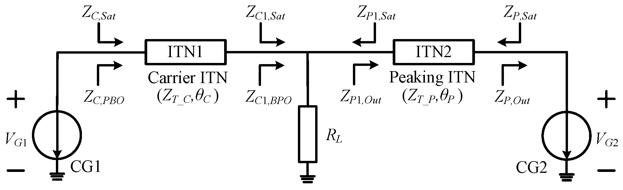
2.1. Dual-Mode DPA Architecture Based on Reciprocal Gate Bias

In this paper, a dual-mode DPA output architecture based on reciprocal bias [44,45] is employed, as illustrated in Figure 2, which enables the DPA to operate effectively in different modes without altering the circuit structure. Table 1 illustrates functions of CG1, CG2, ITN1, and ITN2 in dual-mode operation.
By swapping the gate bias of the two transistors, V G 1 and V G 2 , the roles of the carrier and peaking amplifiers interchange accordingly. In Mode I, the CG1 biased with V G 1 at Class-AB works as the carrier PA, while the CG2 biased with V G 2 at Class-C works as the peaking PA. ITN1 functions as the carrier ITN, facilitating the impedance transformation from Z C 1 , S a t = 2 R L to Z C , S a t = R o p t at saturation and from Z C 1 , P B O = R L to Z C , P B O = 2 R o p t in PBO. Simultaneously, ITN2 functions as the peaking ITN, achieving impedance transformation at saturation from Z P 1 , S a t = 2 R L to Z P , S a t = R o p t , and guaranteeing the output impedance Z P 1 , O u t of the peaking branch in PBO to be infinite.
After the gate biases are swapped, the DPA switches into Mode II, where the CG1 becomes the peaking PA and the CG2 becomes the carrier PA. It should be noted that, although ITN1 and ITN2 in the DPA circuit structure remain unchanged, their functions have been swapped. Specifically, ITN1 now functions as the peaking ITN, while ITN2 functions as the carrier ITN. Due to the different frequency responses of the ITNs in different operating modes, through appropriate design, the DPA can achieve dual-band operation in the same mode, as shown in Figure 2. As a result, the combined operating band of the DPA will be expanded.
During the process of designing the ITNs for the reciprocal gate bias dual-mode DPA, it is necessary to consider the impedance and phase delay requirements in both modes, so as to achieve Doherty operation.

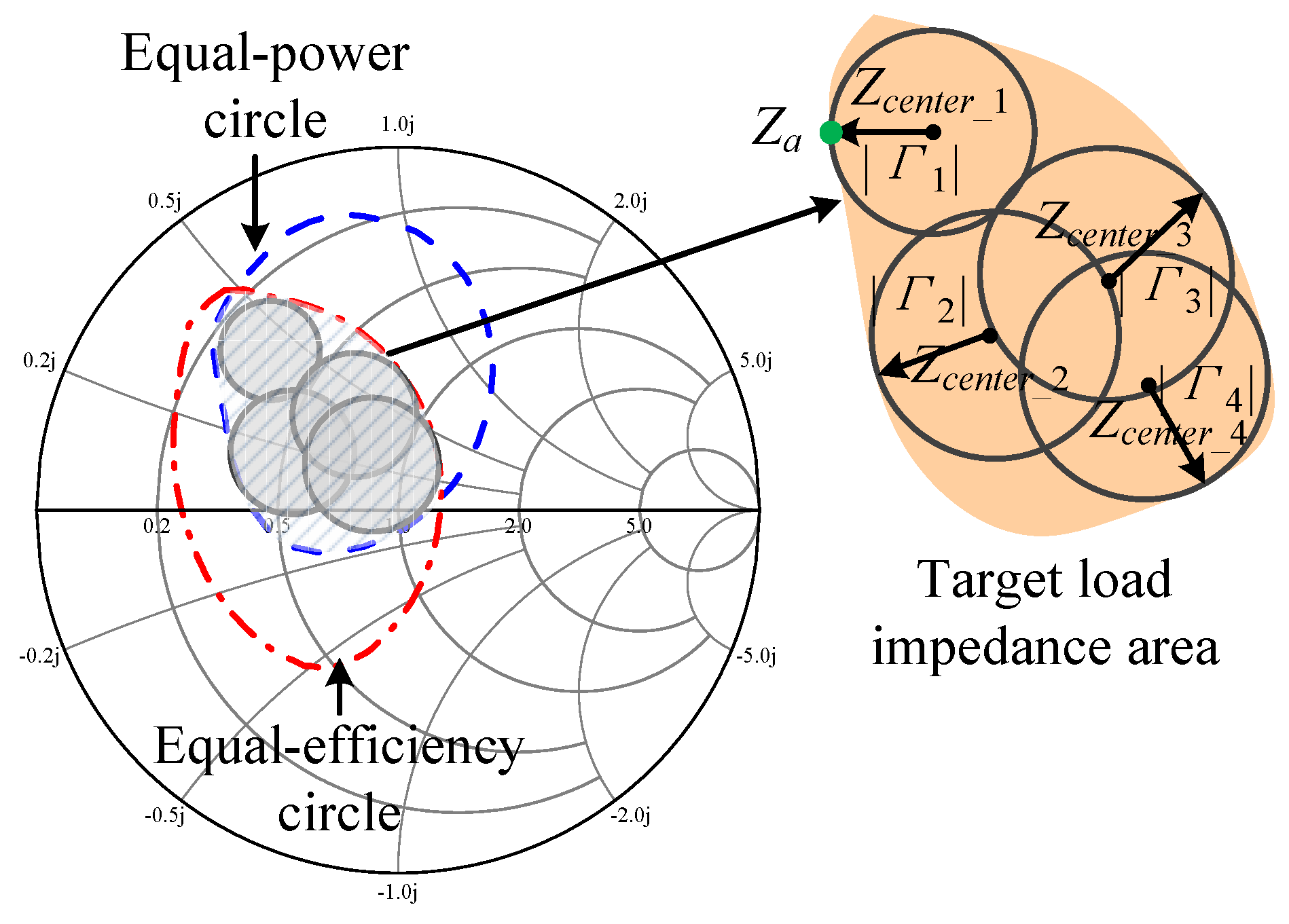
2.2. Load Impedance Region Determination Methods

Load-pull simulation is a commonly used method for obtaining the optimum impedance region. As shown in Figure 3, the overlapping part of the equal-power circles and equal-efficiency circles is the optimum load impedance region. Since the obtained region has an irregular shape, an appropriate method is required to describe it. Conventional impedance constraints are typically calculated using the absolute value of impedance error between the achieved impedance and the target one. To enhance the feasibility of the optimization design, Kong et al. [18] proposed a method based on an inner-tangent circle, which is selected as the optimized target load impedance area. In order to further improve the utilization of the optimum load impedance region, this paper employs multiple impedance constraint circles to describe the region, as shown in Figure 3, where the target load impedance area is expanded compared to previous methods.
To improve the utilization of the optimum load impedance region, this paper employs multiple impedance constraint circles to describe the region, as shown in Figure 3. For each impedance constraint circle, | Γ | represents its radius, which can be calculated by (1):
| Γ | = | Z a Z c e n t e r Z a + Z c e n t e r * |
where Z a represents a point on the impedance constraint circle that is tangent to the optimum impedance region, and Z c e n t e r represents the center of the circle.

2.3. Determination of ITN Phase Delay

The bandwidth of the DPA is significantly influenced by the phase delays of the carrier and peaking ITNs. The schematic of the ideal load modulation network of the DPA is shown in Figure 4. Table A1 in Appendix A summarizes the variable symbols and their definitions in the process of phase delay determination. To achieve the desired impedance transformation, the phase delay θ C of the carrier ITN and the phase delay θ P of the peaking ITN can be expressed by (2) and (3), respectively:
θ C = 90 m × 180
θ P = 180 n × 180
where m and n represent the required phase delay parameters for the carrier ITN and peaking ITN, respectively.
f L and f H are assumed as the design frequencies for the low and high target bands, respectively. According to [33], the phase delay parameters of the ITN are derived as a function of the design frequencies, based on the principle of phase periodicity. Let θ C _ L and θ C _ H represent the phase delay target of the carrier ITN at f L and f H , respectively. Given that the carrier ITN’s phase delay is frequency-dependent, substituting this relationship into (2) yields (4):
θ C _ L : θ C _ H = f L : f H = ( 90 m 1 × 180 ) : ( 90 m 2 × 180 )
where m 1 and m 2 denote the phase delay parameters of the carrier ITN, and they are non-negative integers that satisfy m 2 > m 1 . Similarly, let θ P _ L and θ P _ H represent the phase delay target of the peaking ITN at f L and f H , respectively. Substituting the relationship according to [33] into (3) yields (5):
θ P _ L : θ P _ H = f L : f H = ( 180 n 1 × 180 ) : ( 180 n 2 × 180 )
where n 1 and n 2 denote the phase delay parameters of the peaking ITN, and they are non-negative integers, satisfying n 2 > n 1 .
A realizable ITN has different frequency responses at different design frequencies. The phase delay parameters for the carrier and peaking ITNs are expressed as (6) and (7):
m 2 = f H f L m 1 + 1 2 1 2
n 2 = f H f L ( n 1 + 1 ) 1
Once the phase delay parameters for the low and high target bands are determined, the phase delays of the carrier and peaking ITNs can be calculated using (6) and (7). These phase delays will serve as optimization objectives in the design of carrier and peaking ITNs.

2.4. Impedance-and-Phase Constrained Optimization

A schematic for impedance and phase simulation is illustrated in Figure 5, where the phase delay at the CG plane and the impedance at the package plane can be obtained simultaneously. Through the aforementioned analysis of the required impedance and phase delay for the dual-mode multi-band DPA, this paper proposes a design approach based on impedance-and-phase constrained optimization. This approach can effectively reduce the complexity associated with the design of dual-mode multi-band DPA. Table A1 summarizes the variable symbols and their definitions for impedance-and-phase constrained optimization.
Assuming that the frequencies f I _ L , f I _ H , f I I _ L , and f I I _ H are the design frequencies for lower and upper bands in two modes, respectively, the ITN in Mode I serves as the carrier ITN, with phase delay targets θ I _ L and θ I _ H , according to (2), while it serves as the peaking ITN in Mode II, with phase delay targets θ I I _ L and θ I I _ H according to (3). Consequently, the phase delay optimization objective function for the ITN is formulated as shown in (8):
F θ ( θ I L , θ I H , θ I I L , θ I I H ) = max θ I L θ I _ L 40 , θ I H θ I _ H 40 , θ I I L θ I I _ L 40 , θ I I H θ I I _ H 40
where θ I L , θ I H , θ I I L and θ I I H represent the ITN phase delays to be optimized at the corresponding design frequencies in Mode I and Mode II, respectively. When the maximum value of F θ is less than 1, the deviations between the phase delay of the designed ITN and targets meet specific requirements. To obtain the optimal load impedance for the design frequencies f I _ L , f I _ H , f I I _ L , and f I I _ H , appropriate impedance constraint circles are selected to characterize the target impedance regions at different frequencies as illustrated in Figure 3. The impedance optimization objective function for ITN1 at each design frequency is expressed in (9):
F Γ _ b ( Z b ) = min 1 | Γ | Z b Z c e n t e r _ 1 Z b + Z c e n t e r _ 1 * , , 1 | Γ | Z b Z c e n t e r _ n Z b + Z c e n t e r _ n * ( b = I _ L , I _ H , I I _ L , I I _ H )
where Z c e n t e r _ 1 to Z c e n t e r _ n represent the centers of reflection coefficient constraint circles, and | Γ 1 | to | Γ n | denote the radii of these circles. Z b represents the load impedance of the ITN, where the subscript k can take values I _ L , I _ H , I I _ L , and I I _ H , corresponding to the four design frequencies. When the minimum value of F Γ _ b is less than 1, it indicates that Z b falls within at least one selected impedance constraint circle, achieving optimization. Notably, the impedance optimization objective has been achieved. To ensure that the ITN simultaneously satisfies the impedance constraint requirements at each design frequency, the impedance optimization objective function is designed as shown in (10):
F Γ = max F Γ _ I _ L ( Z I _ L ) , F Γ _ I _ H ( Z I _ H ) , F Γ _ I I _ L ( Z I I _ L ) , F Γ _ I I _ H ( Z I I _ H )
where Z I _ L , Z I _ H , Z I I _ L , and Z I I _ H represent the impedances of ITNs that need to be optimized in dual-mode multi-band operation. When the maximum value of F Γ is less than 1, it indicates that the impedance values of the OMN at each operating frequency have been optimized to fall within the target impedance region.
By combining (8) and (10), the impedance-and-phase constrained optimization objective function is formulated as shown in (11):
F = max ( F θ , F Γ )
When the impedance-and-phase constrained optimization objective function F converges to a value less than 1, it signifies that the ITN has successfully achieved the design objectives.
In order to achieve better performance, various optimization methods have been widely applied to numerous engineering problems [46,47,48,49,50,51,52,53,54]. Therefore, to further enhance both the global optimization efficiency of complex systems and the dynamic adaptability of algorithms, the adaptive particle swarm optimization (APSO) is proposed. The flow chart of the above optimization design process is illustrated in Figure 6. Initially, the ITN topology is determined, and then, the APSO parameters, such as population size, number of iterations, and initial population, are initialized, in which each particle in the population corresponds to the design variables of the ITN (i.e., the width and length of microstrip lines). Subsequently, each particle is transferred to an Advanced Design System (ADS) through an interface program to generate the ITN topology, and S-parameter simulation is performed to obtain the impedance and phase corresponding to the generated ITN. Following this, the simulated results are transferred to MATLAB 2022 through the interface program, after which they are evaluated using the proposed impedance-and-phase optimization objective function. The iteration of APSO continues until the optimization objective is satisfied.
In summary, the proposed dual-mode multi-band DPA utilizes reciprocal gate bias to switch between operating modes, thereby extending the operational frequency bands. Based on load-pull simulations, multiple impedance constraint circles are introduced to encompass optimal load impedance regions. Phase delay targets are derived from the principle of phase periodicity. Subsequently, the optimization design of ITNs is processed with impedance and phase constraints using APSO. This approach enables high-efficiency operation across all designated frequency bands in both modes.

3. Design and Simulation of Dual-Mode Multi-Band DPA

To verify the proposed design method, a dual-mode multi-band DPA is designed and simulated using Wolfspeed CGH40010F GaN transistors. The center frequencies are selected as 2.0 and 2.8 GHz in Mode I, and 2.5 and 3.3 GHz in Mode II, due to the presence of a large number of commonly used communication frequency bands in their vicinity. The relevant details are elaborated in the Introduction section. Rogers 4350, a dielectric substrate material with a relative dielectric constant of 3.66 and a thickness of 30 mils, is chosen for this design.

3.1. Determination of the Impedance Constraint Region

Considering that the dual-mode multi-band DPA operates at center frequencies of 2.0, 2.8, 2.5, and 3.3 GHz, load-pull simulations are performed for these four frequencies, as illustrated in Figure 7. For each optimum impedance region, four impedance constraint circles are introduced to maximize utilization. The centers Z c e n t e r _ 1 to Z c e n t e r _ 4 and radii | Γ 1 | to | Γ 4 | of these circles are detailed in Table 2. This approach effectively describes the impedance target region in the impedance-and-phase constrained optimization. Since the transistors used in both branches of the dual-mode multi-band DPA are identical, the target impedance regions for the ITNs of both circuits at saturation can be accurately characterized using this method.

3.2. Determination of Phase Delays of Carrier and Peaking ITNs
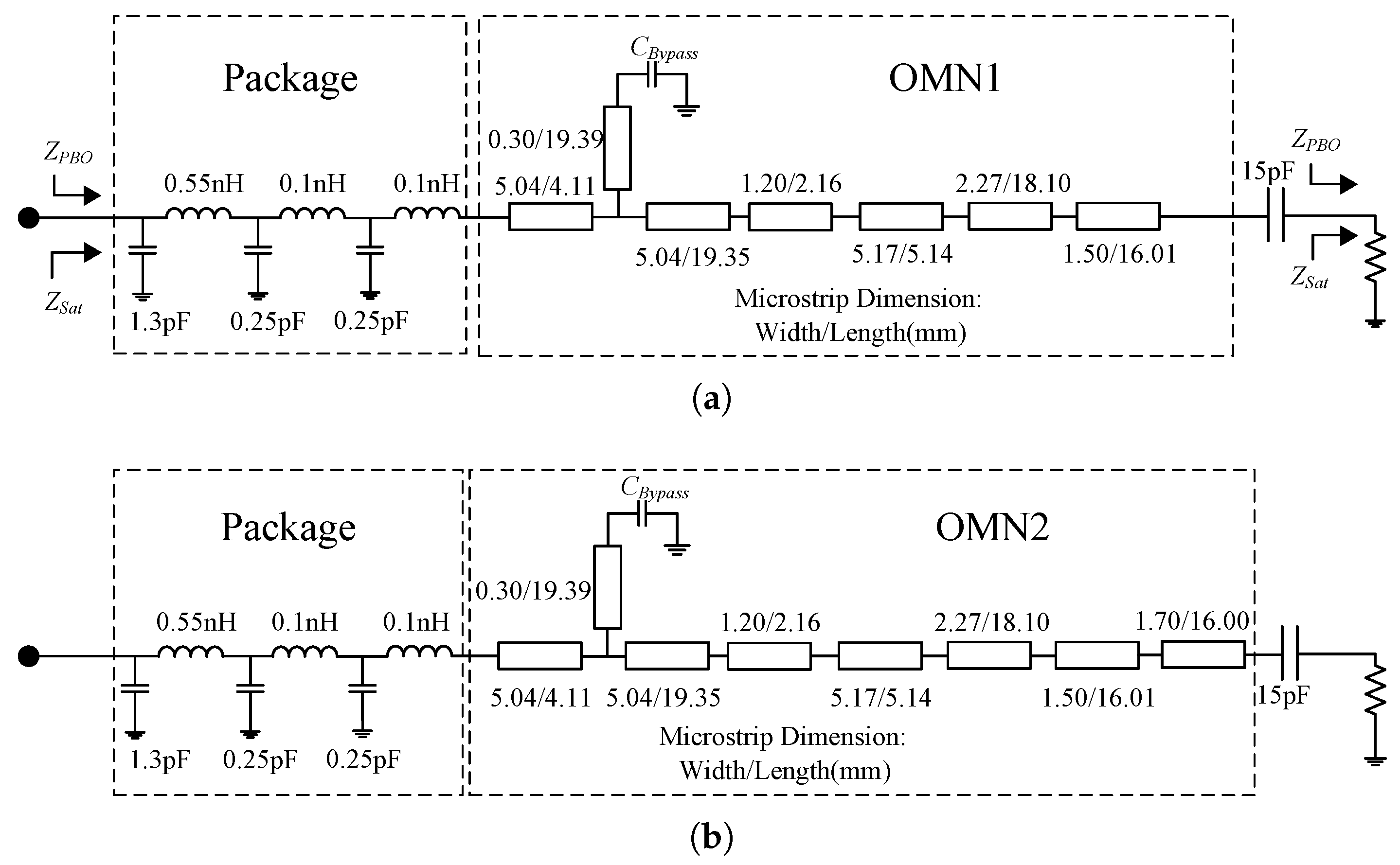
Once the design frequencies have been determined, the phase delay parameters of the carrier and peaking ITNs can be calculated using (4) and (5). Given that m and n are integers, the values of n 2 and m 2 , calculated using (6) and (7), must be rounded after selecting n 1 and m 1 . The required phase delay targets for ITN1 and ITN2 are summarized in Table 3 for the dual-mode multi-band DPA operating at 2.0, 2.8, 2.5, and 3.3 GHz. By applying this method, the phase delay targets for the carrier and peaking ITNs within the target frequency bands can be accurately determined.

3.3. Design of ITNs

Considering the phase delay requirements for the carrier and peaking ITNs of the dual-mode multi-band DPA across the two operating modes, the design process initially focuses on the carrier ITN for Mode I.
Using the impedance-and-phase constrained optimization design described in Section 2.4, multiple optimization iterations are carried out to guarantee that ITN1 satisfies the desired impedance and phase delay requirements at saturation and in the PBO state. The ITN1 topology to be optimized is shown in Figure 8, together with the objective function values of the best individual at each iteration to illustrate the optimization process. As the iterations proceed, the objective function value converges and stabilizes after approximately 20 iterations, indicating that these design variables successfully meet the design target. Additionally, the ITN topology generated by the set of variables in the best individual which satisfies the requirements for impedance matching and phase delay has been obtained, and the values of these variables are presented in Table 4. The phase delay variation curves of the 10th, 30th, and 50th individuals at the four operating frequencies (2.0, 2.5, 2.8, and 3.3 GHz) are shown in Figure 9, indicating that the phase delays of the selected individuals at the four target frequencies fulfill the phase delay requirements for ITN1 in the dual-mode multi-band DPA, which confirms the consistency and validity of the optimization across the population.
The designed ITN1 structure is presented in Figure 10a. Since ITN2 and ITN1 in the reciprocal-bias dual-mode multi-band DPA have a similar structure, ITN2 is designed by adding a phase compensation line after ITN1. The corresponding schematic is shown in Figure 10b.
After the impedance-and-phase constrained optimization design is completed, Figure 11 depicts the resulting phase delays of ITN1 and ITN2 at their respective design operating frequencies. When the reciprocal-bias dual-mode multi-band DPA operates in Mode I, ITN1 functions as the carrier ITN. At 2.0 and 2.8 GHz, its phase delays are 301 and 449 , respectively. Meanwhile, ITN2 acts as the peaking ITN, with phase delays of 355 and 525 at 2.0 and 2.8 GHz, correspondingly. Upon swapping the gate bias, the DPA switches to Mode II. In this mode, ITN2 serves as the carrier ITN, presenting phase delays of 464 and 630 at 2.5 and 3.3 GHz, respectively. ITN1 functions as the peaking ITN, with phase delays of 397 and 540 at 2.5 and 3.3 GHz, respectively. These results are consistent with the theoretical analysis.
The optimized trajectory achieved by the optimized OMN and the optimal impedance regions at four frequencies are shown in Figure 12. The impedance at 2.0 and 2.8 GHz in Mode I, as well as at 2.5 and 3.3 GHz in Mode II, is all located within the optimum load impedance region. This confirms that the design meets the expected objectives.

3.4. Simulation Results of Dual-Mode Multi-Band DPA

The performance of the dual-mode multi-band DPA is simulated under different operating modes, and the results are presented in Figure 13. In Mode I, the designed DPA functions within the frequency bands of 1.96–2.10 and 2.75–2.86 GHz. At saturation, its drain efficiencies (DEs) are 57.0–62.5% and 52.4–57.4%, respectively. The 6 dB PBO DEs span from 51.4 to 55.9% and 52.4 to 54.0%.
In Mode II, the DPA operates within the frequency bands of 2.49–2.61 and 3.20–3.36 GHz. At saturation, the DEs reach 59.2–69.6% and 64.3–67.5%, respectively. The 6 dB PBO DEs range from 51.6 to 55.7% and 51.8 to 58.6%, respectively.
Figure 14 illustrates the simulated gain and efficiency versus output power at the center operating frequencies for both Mode I and Mode II. At saturation, the output power at the four design frequencies exceeds 43 dBm, while the 6 dB PBO efficiency is over 50%, demonstrating a satisfactory performance. In addition, the simulated load modulation trajectories at the CG plane of the devices are plotted in Figure 15. The results show that the designed DPA can achieve appropriate Doherty load modulation for both carrier and peaking amplifiers.

4. Fabrication and Measurement of Dual-Mode Multi-Band DPA

To further validate the design, the dual-mode multi-band DPA was fabricated. A photograph of the DPA is shown in Figure 16a. To evaluate its performance, the fabricated DPA was measured with continuous wave and modulated signals. The measurement was carried out across the frequency bands of 1.96–2.10 GHz and 2.75–2.86 GHz for Mode I, and 2.49–2.61 GHz and 3.20–3.36 GHz for Mode II, with the setup presented in Figure 16b. The drain bias voltages of the carrier and peaking PAs are both 28 V. The gate bias voltage of the carrier PA is −3 V, and that of the peaking PA is −6 V. For the selected transistor, the DC quiescent current ( I d q ) of the carrier PA is 0.1 A.

4.1. Continuous Wave Measurement

The measured efficiency and gain versus output power of the dual-mode multi-band DPA are presented in Figure 17. The DPA maintains high efficiency in both saturation and PBO state. Figure 18 illustrates measured and simulated DE and output power versus frequency in Mode I and Mode II.
In Mode I, for the bands of 1.96–2.10 and 2.75–2.86 GHz, in the 6 dB PBO state, the DPA attains DEs of 49.4–55.7% and 49.8–51.7%, respectively. At saturation, the DEs are in the range of 55.2–62.5% and 53.7–60.0%.
In Mode II, for the bands of 2.49–2.61 and 3.20–3.36 GHz, for the 6 dB PBO state, the DPA attains DEs of 51.2% to 52.4% and 50.4% to 53.5%. At saturation, the DEs are in the range of 60.0–68.6% and 60.2–63.5%, respectively.
The experimental results are appropriately consistent with the simulation results, validating the effectiveness of the proposed design methodology.

4.2. Modulated Signal Measurement

To evaluate the performance of the DPA, an LTE signal with a PAPR of 6.5 dB and a bandwidth of 20 MHz was used for measurement. To meet the linearity requirements for wireless communication systems, digital predistortion (DPD) was applied to the DPA. The piecewise second-order dynamic deviation reduction model was used in the DPD modeling [55]. The magnitude threshold was set as 0.4 0.7 for the normalized data, while the nonlinearity order was selected as {7, 7, 7} and the memory length was set to {3, 3, 3}. Figure 19 presents the measured results of the adjacent channel leakage ratio (ACLR) before and after DPD implementation at the designed operating frequencies. As shown in the figure, the ACLR values are consistently around −50 dBc after DPD. The average output power ranges from 36 to 37 dBm, with DEs exceeding 50%.
Figure 20 illustrates the output spectra of the four design operating frequencies before and after DPD. After DPD, ACLR performance reaches approximately −50 dBc, indicating a significant improvement in the nonlinear effects of the DPA.
Table 5 compares the proposed DPA with the published multi-band or multi-mode DPAs measured under a continuous wave signal. The results demonstrate that the proposed DPA exhibits satisfactory performance.

5. Conclusions

This paper proposes a dual-mode multi-band DPA design method employing impedance-and-phase constrained optimization based on reciprocal gate bias. By swapping the gate bias of the two transistors, the roles of the carrier and peaking amplifiers interchange accordingly. A dual-mode multi-band DPA operating in Mode I at 1.96–2.10 GHz and 2.75–2.86 GHz, and in Mode II at 2.49–2.61 GHz and 3.20–3.36 GHz, is designed and fabricated. The measured results show that this DPA can achieve high DEs at saturation and PBO states within all the operating frequency bands, making it suitable for future wireless communication systems. Experimental results confirm that the DPA achieves high drain efficiency at both saturation and PBO levels across all bands, demonstrating strong potential for deployment in next-generation wireless communication systems.

Author Contributions

Methodology, M.T. and Y.C.; software, S.N.; validation, Z.Z. and S.N.; resources, J.X.; writing—original draft preparation, M.T.; writing—review and editing, W.K.; supervision, W.K.; project administration, W.K. All authors have read and agreed to the published version of the manuscript.

Funding

This work was supported by the National Natural Science Foundation of China (Grant No. 62171204 and 62001192).

Data Availability Statement

Data are available on request from the authors.

Conflicts of Interest

The authors declare no conflicts of interest.

Abbreviations

The following abbreviations are used in this manuscript:
APSOAdaptive particle swarm optimization
ADSAdvanced design system
CGCurrent generator
DEDrain efficiency
DPADoherty power amplifier
DPDDigital predistortion
ITNImpedance transformation network
LMNLoad modulation network
OMNOutput matching network
PAPower amplifier
PAPRPeak-to-average power ratio
PBOPower back-off
PMNPost-matching network

Appendix A

To facilitate the analysis of the dual-mode multi-band DPA optimization design theory discussed in Section 2, all relevant variables are compiled in Table A1 of Appendix A for easy reference.
Table A1. Variable symbols and definitions.
Variable SymbolDefinition
θ C Target phase delay for the carrier ITN.
θ P Target phase delay for the peaking ITN.
mPhase delay parameter for the carrier ITN.
nPhase delay parameter for the peaking ITN.
f L Design frequency of the low target band.
f H Design frequency of the high target band.
θ C _ L Target phase delay of the carrier ITN at f L .
θ C _ H Target phase delay of the carrier ITN at f H .
θ P _ L Target phase delay of the peaking ITN at f L .
θ P _ H Target phase delay of the peaking ITN at f H .
m 1 Phase delay parameter of the carrier ITN at f L .
m 2 Phase delay parameter of the carrier ITN at f H .
n 1 Phase delay parameter of the peaking ITN at f L .
n 2 Phase delay parameter of the peaking ITN at f H .
F θ Phase delay optimization objective function.
θ I L ITN phase delay at f I _ L in Mode I.
θ I H ITN phase delay at f I _ H in Mode I.
θ I I L ITN phase delay at f I I _ L in Mode II.
θ I I H ITN phase delay at f I I _ H in Mode II.
θ I _ L Target phase delay for the ITN at f I _ L in Mode I.
θ I _ H Target phase delay for the ITN at f I _ H in Mode I.
θ I I _ L Target phase delay for the ITN at f I I _ L in Mode II.
θ I I _ H Target phase delay for the ITN at f I I _ H in Mode II.
Z b Load impedance of the ITN at a specific design frequency.
Z c e n t e r _ 1 Center impedance of the first impedance constraint circle.
| Γ 1 | Radius of the first impedance constraint circle.
Z c e n t e r _ n Center impedance of the n-th impedance constraint circle.
| Γ n | Radius of the n-th impedance constraint circle.
F Γ Comprehensive impedance optimization objective function.
FTotal optimization objective function.

References

  1. Pitt, A.; Jindal, G.; Morris, K.; Cappello, T. A Broadband Asymmetrical Doherty Power Amplifier with Optimized Continuous Mode Harmonic Impedances. IEEE J. Microw. 2023, 3, 1120–1133. [Google Scholar] [CrossRef]
  2. Xia, J.; Yang, M.; Guo, Y.; Zhu, A. A Broadband High-Efficiency Doherty Power Amplifier with Integrated Compensating Reactance. IEEE Trans. Microw. Theory Tech. 2016, 64, 2014–2024. [Google Scholar] [CrossRef]
  3. Liu, T.; Wang, X.; Xin, Y.; Yang, X. PAPR Suppression for Angular-Domain-Based Massive Multiple-Input Multiple-Output Orthogonal Frequency Division Multiplexing System. Electronics 2023, 12, 4015. [Google Scholar] [CrossRef]
  4. Que, X.; Li, J.; Wang, Y. A Broadband Three-Way Series Doherty Power Amplifier with Deep Power Back-Off Efficiency Enhancement for 5G Application. Electronics 2024, 13, 1882. [Google Scholar] [CrossRef]
  5. Li, G.; Xu, W.; Nan, J.; Gao, M. Design of Efficient Concurrent Dual-Frequency Doherty Power Amplifier Based on Step Impedance Low-Pass Filter. Electronics 2023, 12, 4092. [Google Scholar] [CrossRef]
  6. Neveux, G.; Hallepee, C.; Passerieux, D.; Barataud, D. Non-Linear Simulation by Harmonic Balance Techniques of Load Modulated Power Amplifier Driven by Random Modulated Signals. Electronics 2024, 13, 947. [Google Scholar] [CrossRef]
  7. Kong, W.; Xia, J.; Zhou, X.; Zhang, T.; Zhang, W.; Bao, X. Bandwidth Extension of Three-Way Doherty Power Amplifier with Reactance Compensation Using Parallel Peaking Amplifiers. IEEE Access 2021, 9, 91661–91669. [Google Scholar] [CrossRef]
  8. Xia, J.; Xie, Z.; Kong, W.; Liu, R.; Zhao, Z.; Zhu, X.W. A 9 dB back-off dual-band asymmetric Doherty power amplifier using dual peaking amplifiers for reactance compensation. Microw. Opt. Technol. Lett. 2022, 64, 1145–1153. [Google Scholar] [CrossRef]
  9. Mehter, E.; Üçüncü, M. Radio Frequency (RF) Power Amplifier Design Providing High Power Efficiency in a Wide Dynamic Range. Electronics 2025, 14, 1435. [Google Scholar] [CrossRef]
  10. Moreno Rubio, J.J.; Noori, A. Doherty Power Amplifier Design via Differential Combining. Electronics 2024, 13, 3961. [Google Scholar] [CrossRef]
  11. Liu, H.Y.; Zhai, C.; Cheng, K.K.M. Novel Dual-Band Equal-Cell Doherty Amplifier Design with Extended Power Back-Off Range. IEEE Trans. Microw. Theory Tech. 2020, 68, 1012–1021. [Google Scholar] [CrossRef]
  12. Cui, H.; Leung, V.C.M.; Li, S.; Wang, X. LTE in the Unlicensed Band: Overview, Challenges, and Opportunities. IEEE Wirel. Commun. 2017, 24, 99–105. [Google Scholar] [CrossRef]
  13. Hussain, A.; Kildal, P.S.; Glazunov, A.A. Interpreting the Total Isotropic Sensitivity and Diversity Gain of LTE-Enabled Wireless Devices From Over-the-Air Throughput Measurements in Reverberation Chambers. IEEE Access 2015, 3, 131–145. [Google Scholar] [CrossRef]
  14. Shin, J.; Choi, W.; Chen, Y.; Jeon, H.; Bae, S.; Choi, Y.C.; Kang, H.; Koo, H.; Woo, Y.Y.; Lee, K.Y.; et al. Broadband Virtual-Stub Doherty Power Amplifier Using Asymmetric Structure. IEEE Access 2023, 11, 101425–101434. [Google Scholar] [CrossRef]
  15. Ahn, J.; Youn, Y.; Kim, B.; Lee, J.; Choi, N.; Lee, Y.; Kim, G.; Hong, W. Wideband 5G N77/N79 4 × 4 MIMO Antenna Featuring Open and Closed Stubs for Metal-Rimmed Smartphones with Four Slits. IEEE Antennas Wirel. Propag. Lett. 2023, 22, 2798–2802. [Google Scholar] [CrossRef]
  16. Sim, C.Y.D.; Liu, H.Y.; Huang, C.J. Wideband MIMO Antenna Array Design for Future Mobile Devices Operating in the 5G NR Frequency Bands n77/n78/n79 and LTE Band 46. IEEE Antennas Wirel. Propag. Lett. 2020, 19, 74–78. [Google Scholar] [CrossRef]
  17. Eid, M.A.E.; Abouelnaga, T.G.; Ibrahim, H.A.; Hamad, E.K.I.; Al-Gburi, A.J.A.; Alghamdi, T.A.H.; Alathbah, M. Highly Efficient GaN Doherty Power Amplifier for N78 Sub-6 GHz Band 5G Applications. Electronics 2023, 12, 4001. [Google Scholar] [CrossRef]
  18. Kong, W.; Zhong, Y.; Xia, J.; Zhou, X.Y.; Fu, H.; Dong, W.; Zhao, Z.M.; Zhu, X.W. Optimization Design of Broadband Doherty PA Using Fragment-Type Matching Network Based on Dual-State Impedance Objective Function. IEEE Trans. Circuits Syst. II Express Briefs 2024, 71, 1809–1813. [Google Scholar] [CrossRef]
  19. Nikandish, G.; Staszewski, R.B.; Zhu, A. Breaking the Bandwidth Limit: A Review of Broadband Doherty Power Amplifier Design for 5G. IEEE Microw. Mag. 2020, 21, 57–75. [Google Scholar] [CrossRef]
  20. Yang, Z.; Li, M.; Yao, Y.; Dai, Z.; Li, T.; Jin, Y. Design of Concurrent Dual-Band Continuous Class-J Mode Doherty Power Amplifier with Precise Impedance Terminations. IEEE Microw. Wirel. Compon. Lett. 2019, 29, 348–350. [Google Scholar] [CrossRef]
  21. Ren, M.; Gao, R.; Liu, S.; Li, M.; Shi, W.; Dai, Z.; Chen, S.; Pang, J. Design of Wideband Doherty Power Amplifier Using Inverse Continuous Class-F Mode. IEEE Trans. Circuits Syst. II Express Briefs 2024, 71, 4176–4180. [Google Scholar] [CrossRef]
  22. Abounemra, A.M.E.; Helaoui, M.; Ghannouchi, F.M. Design of an efficiency enhanced wideband Doherty power amplifier based on synthesising of a modified harmonic-control load modulation network. IET Microw. Antennas Propag. 2024, 18, 356–368. [Google Scholar] [CrossRef]
  23. Bai, G.; Dai, Z.; Wang, J.; Bi, C.; Shi, W.; Pang, J.; Li, M. Design of Broadband Doherty Power Amplifier Based on Single Loop Load Modulation Network. IEEE J. Emerg. Sel. Top. Circuits Syst. 2024, 14, 122–132. [Google Scholar] [CrossRef]
  24. Chen, Y.; Choi, W.; Shin, J.; Jeon, H.; Bae, S.; Bae, K.; Song, J.; Ju, Y.; Oh, H.; Kang, H.; et al. Comprehensive Analysis of Coupled Transmission Lines for Broadband High-Efficiency Doherty Power Amplifiers. IEEE Trans. Microw. Theory Tech. 2025; early access. [Google Scholar] [CrossRef]
  25. Alsulami, R.; Roblin, P.; Martinez-Lopez, J.I.; Hahn, Y.; Liang, C.; Popovic, Z.; Chen, V. A Novel 3-Way Dual-Band Doherty Power Amplifier for Enhanced Concurrent Operation. IEEE Trans. Microw. Theory Tech. 2021, 69, 4041–4058. [Google Scholar] [CrossRef]
  26. Guo, X.; Ye, J.; Wu, W. Dual-Band Class-X Doherty Power Amplifier with Large Frequency Ratio. IEEE Microw. Wirel. Technol. Lett. 2024, 34, 643–646. [Google Scholar] [CrossRef]
  27. Chen, X.; Chen, W.; Ghannouchi, F.M.; Feng, Z.; Liu, Y. A Broadband Doherty Power Amplifier Based on Continuous-Mode Technology. IEEE Trans. Microw. Theory Tech. 2016, 64, 4505–4517. [Google Scholar] [CrossRef]
  28. Chen, W.; Zhang, S.; Liu, Y.; Liu, Y.; Ghannouchi, F.M. A Concurrent Dual-Band Uneven Doherty Power Amplifier with Frequency-Dependent Input Power Division. IEEE Trans. Circuits Syst. I Regul. Pap. 2014, 61, 552–561. [Google Scholar] [CrossRef]
  29. Kalyan, R.; Rawat, K.; Koul, S.K. A Digitally Assisted Dual-Input Dual-Band Doherty Power Amplifier with Enhanced Efficiency and Linearity. IEEE Trans. Circuits Syst. II Express Briefs 2019, 66, 297–301. [Google Scholar] [CrossRef]
  30. Rawat, K.; Ghannouchi, F.M. Design Methodology for Dual-Band Doherty Power Amplifier with Performance Enhancement Using Dual-Band Offset Lines. IEEE Trans. Ind. Electron. 2012, 59, 4831–4842. [Google Scholar] [CrossRef]
  31. Jiang, S.; Liu, G.; You, M.; Wu, Y. A novel dual-band forward/inverse Doherty power amplifier. Int. J. Circuit Theory Appl. 2024, 52, 6073–6082. [Google Scholar] [CrossRef]
  32. Zhou, L.H.; Zhou, X.Y.; Chan, W.S. Compact Dual-Passband Doherty Power Amplifier Based on Stub-Loaded Stepped-Impedance Transformer. IEEE Trans. Circuits Syst. I Regul. Pap. 2024, 71, 99–109. [Google Scholar] [CrossRef]
  33. Kong, W.; Chen, Y.; Xia, J.; Ni, Z.; Ni, S.; Zhang, W.; Zhu, X.W. Design of Tri-Band Doherty Power Amplifier Using Phase and Impedance Constrained Optimization. Microw. Opt. Technol. Lett. 2025, 67, e70100. [Google Scholar] [CrossRef]
  34. Tang, Y.; Feng, W.; Zhou, X.; Wang, W.; Gu, L.; Xue, Q.; Che, W. Broadband High-Efficiency Dual-Mode Doherty Power Amplifier Using Hybrid F/F–1 Continuous-Mode Technology. IEEE Trans. Circuits Syst. I Regul. Pap. 2023, 70, 2651–2664. [Google Scholar] [CrossRef]
  35. Han, Y.; Gao, R.; Liu, S.; Li, M.; Shi, W.; Dai, Z.; Chen, S.; Pang, J. Enhanced Dual-Mode Reciprocal Doherty Power Amplifier Using Modified Combining Load and Parameter Sweeping Analysis. IEEE Trans. Circuits Syst. I Regul. Pap. 2024, 71, 3086–3097. [Google Scholar] [CrossRef]
  36. Liu, S.; Pang, J.; Gao, R.; Yao, T.; Cai, T.; Li, M.; Shi, W.; Dai, Z. Triple-Mode Reciprocal Doherty Power Amplifier with Multi-Band Operation and Extended High Efficiency Range. IEEE Trans. Circuits Syst. I Regul. Pap. 2023, 70, 1928–1939. [Google Scholar] [CrossRef]
  37. Qu, Y.; Crupi, G.; Cai, J. A Broadband PA Design Based on Bayesian Optimization Augmented by Dynamic Feasible Region Shrinkage. IEEE Microw. Wirel. Compon. Lett. 2022, 32, 1139–1142. [Google Scholar] [CrossRef]
  38. Chen, P.; Xia, J.; Merrick, B.M.; Brazil, T.J. Multiobjective Bayesian Optimization for Active Load Modulation in a Broadband 20-W GaN Doherty Power Amplifier Design. IEEE Trans. Microw. Theory Tech. 2017, 65, 860–871. [Google Scholar] [CrossRef]
  39. Mengozzi, M.; Gibiino, G.P.; Angelotti, A.M.; Santarelli, A.; Florian, C.; Colantonio, P. Automatic Optimization of Input Split and Bias Voltage in Digitally Controlled Dual-Input Doherty RF PAs. Energies 2022, 15, 4892. [Google Scholar] [CrossRef]
  40. Ni, Z.; Xia, J.; Zhou, X.; Kong, W.; Zhang, H.; Yu, C.; Zhu, X.W. Design and Analysis of Optimization Method for Ultra-Wideband PA Based on Improved MOEA/D Algorithm Using Mixed Objective Function. IEEE Trans. Comput.-Aided Des. Integr. Circuits Syst. 2024; early access. [Google Scholar] [CrossRef]
  41. Hao, Z.; Qu, Y.; Huang, J.; Crupi, G.; Cai, J. Automatic multi-objective particle swarm optimization method for effective Doherty power amplifier design. Int. J. Numer. Model. Electron. Netw. Devices Fields 2024, 37, e3204. [Google Scholar] [CrossRef]
  42. Li, C.; You, F.; Yao, T.; Wang, J.; Shi, W.; Peng, J.; He, S. Simulated Annealing Particle Swarm Optimization for High-Efficiency Power Amplifier Design. IEEE Trans. Microw. Theory Tech. 2021, 69, 2494–2505. [Google Scholar] [CrossRef]
  43. Fan, Z.; Hao, Z.; Huang, J.; Cai, J. Design of RF-Input Sequential LMBA Using PSO Algorithm with Improved Linear Self-Adaptive Hyper-Parameters. IEEE Trans. Microw. Theory Tech. 2024, 72, 6414–6425. [Google Scholar] [CrossRef]
  44. Li, M.; Pang, J.; Li, Y.; Zhu, A. Ultra-Wideband Dual-Mode Doherty Power Amplifier Using Reciprocal Gate Bias for 5G Applications. IEEE Trans. Microw. Theory Tech. 2019, 67, 4246–4259. [Google Scholar] [CrossRef]
  45. Pang, J.; Dai, Z.; Li, Y.; Li, M.; Zhu, A. Multiband Dual-Mode Doherty Power Amplifier Employing Phase Periodic Matching Network and Reciprocal Gate Bias for 5G Applications. IEEE Trans. Microw. Theory Tech. 2020, 68, 2382–2397. [Google Scholar] [CrossRef]
  46. Jiang, H.; Xu, W.; Chen, Q. Evaluating aroma quality of black tea by an olfactory visualization system: Selection of feature sensor using particle swarm optimization. Food Res. Int. 2019, 126, 108605. [Google Scholar] [CrossRef] [PubMed]
  47. Bai, S.; Yang, Q.; Niu, K.; Zhao, B.; Zhou, L.; Yuan, Y. Discrete element-based optimization parameters of an experimental corn silage crushing and throwing device. Trans. ASABE 2021, 64, 1019–1026. [Google Scholar] [CrossRef]
  48. Pang, Y.; Li, H.; Tang, P.; Chen, C. Synchronization optimization of pipe diameter and operation frequency in a pressurized irrigation network based on the genetic algorithm. Agriculture 2022, 12, 673. [Google Scholar] [CrossRef]
  49. Li, Y.; Xu, L.; Gao, Z.; Lu, E.; Li, Y. Effect of vibration on rapeseed header loss and optimization of header frame. Am. Soc. Agric. Biol. Eng. 2021, 64, 1247–1258. [Google Scholar] [CrossRef]
  50. Yang, Q.; Cai, J.; Zhou, X.; Ahamd, I.; Hu, J.; Gu, J. The optimization of topological mechanism and dimension design of parallel transplanting machine in greenhouse. AMA Agric. Mech. Asia Afr. Lat. Am. 2021, 52, 61–66. Available online: https://www.cabidigitallibrary.org/doi/full/10.5555/20220472230 (accessed on 2 November 2022).
  51. Ayim, I.; Ma, H.; Alenyorege, E.A. Optimizing and predicting degree of hydrolysis of ultrasound assisted sodium hydroxide extraction of protein from tea (Camellia sinensis L.) residue using response surface methodology. J. Food Sci. Technol.-Mysore 2018, 55, 5166–5174. [Google Scholar] [CrossRef]
  52. Xu, F.; Wang, B.; Hong, C.; Telebielaigen, S.; Nsor-Atindana, J.; Duan, Y.; Zhong, F. Optimization of spiral continuous flow-through pulse light sterilization for Escherichia coli in red grape juice by response surface methodology. Food Control 2019, 105, 8–12. [Google Scholar] [CrossRef]
  53. Bonah, E.; Huan, X.; Yi, R.; Aheto, J.H.; Osae, R.; Golly, M. Electronic nose classification and differentiation of bacterial foodborne pathogens based on support vector machine optimized with particle swarm optimization algorithm. J. Food Process Eng. 2019, 42, e13236. [Google Scholar] [CrossRef]
  54. Tang, N.; Sun, J.; Yao, K.; Zhou, X.; Tian, Y.; Cao, Y.; Nirere, A. Identification of Lycium barbarum varieties based on hyperspectral imaging technique and competitive adaptive reweighted sampling-whale optimization algorithm-support vector machine. J. Food Process Eng. 2021, 44, e13603. [Google Scholar] [CrossRef]
  55. Xia, J.; Chen, W.; Meng, F.; Yu, C.; Zhu, X. Improved Three-Stage Doherty Amplifier Design with Impedance Compensation in Load Combiner for Broadband Applications. IEEE Trans. Microw. Theory Tech. 2019, 67, 778–786. [Google Scholar] [CrossRef]
  56. Kalyan, R.; Rawat, K.; Koul, S.K. Reconfigurable and Concurrent Dual-Band Doherty Power Amplifier for Multiband and Multistandard Applications. IEEE Trans. Microw. Theory Tech. 2017, 65, 198–208. [Google Scholar] [CrossRef]
  57. Li, X.; Helaoui, M.; Ghannouchi, F.; Chen, W. A Quad-Band Doherty Power Amplifier Based on T-Section Coupled Lines. IEEE Microw. Wirel. Compon. Lett. 2016, 26, 437–439. [Google Scholar] [CrossRef]
  58. Nghiem, X.A.; Negra, R. Design of a concurrent quad-band GaN-HEMT Doherty power amplifier for wireless applications. In Proceedings of the 2013 IEEE MTT-S International Microwave Symposium Digest (MTT), Seattle, WA, USA, 2–7 June 2013. [Google Scholar] [CrossRef]
Figure 1. Architecture of a conventional DPA.
Electronics 14 02078 g001
Figure 2. Output architecture for dual-mode multi-band DPA and frequency bands in Mode I and Mode II.
Electronics 14 02078 g002
Figure 3. Impedance-optimized region coverage strategy based on multiple impedance constrained circles.
Electronics 14 02078 g003
Figure 4. Schematic of the ideal load modulation network of DPA.
Electronics 14 02078 g004
Figure 5. Schematic for impedance and phase simulation.
Electronics 14 02078 g005
Figure 6. Flow chart for impedance-and-phase constrained optimization.
Electronics 14 02078 g006
Figure 7. Coverage of the target impedance region with impedance constraint circles at four design frequencies: (a) 2.0, (b) 2.8, (c) 2.5, and (d) 3.3 GHz.
Electronics 14 02078 g007
Figure 8. Convergence of the objective function value of the best individual and the ITN to be optimized.
Electronics 14 02078 g008
Figure 9. Phase delay variation curve versus iterations for different individuals.
Electronics 14 02078 g009
Figure 10. Schematic of designed (a) ITN1 and (b) ITN2.
Electronics 14 02078 g010
Figure 11. Simulated results for phase delay of ITNs: (a) ITN1 and (b) ITN2.
Electronics 14 02078 g011
Figure 12. Impedance trajectory achieved by the optimized OMN and the four optimal load impedance regions.
Electronics 14 02078 g012
Figure 13. Simulated efficiency and output power of the dual-mode multi-band DPA at saturation and PBO states in (a) Mode I (around 2.0 and 2.8 GHz) and (b) Mode II (around 2.5 and 3.3 GHz).
Electronics 14 02078 g013
Figure 14. Simulated efficiency and gain versus output power at saturation and PBO in (a) Mode I at 2.0 and 2.8 GHz and (b) Mode II at 2.5 and 3.3 GHz.
Electronics 14 02078 g014
Figure 15. Simulated load modulation trajectories at CG plane of carrier PA and peaking PA in dual-mode operation.
Electronics 14 02078 g015
Figure 16. Dual-mode multi-band DPA (a) photograph and (b) measurement setup.
Electronics 14 02078 g016
Figure 17. Measured efficiency and gain versus output power (a) at 2.0 and 2.8 GHz in Mode I and (b) at 2.5 and 3.3 GHz in Mode II.
Electronics 14 02078 g017
Figure 18. Measured and simulated DE and output power versus frequency in (a) Mode I (around 2.0 and 2.8 GHz) and (b) Mode II (around 2.5 and 3.3 GHz).
Electronics 14 02078 g018
Figure 19. Comparison of ACLR and efficiency before and after DPD.
Electronics 14 02078 g019
Figure 20. Output spectrum of a dual-mode multi-band Doherty amplifier before and after DPDs. (a) Mode I; (b) Mode II.
Electronics 14 02078 g020
Table 1. Functions of CG1, CG2, ITN1, and ITN2 in dual-mode operation.
CG1CG2ITN1ITN2
Mode Icarrier PApeaking PAcarrier ITNpeaking ITN
Mode IIpeaking PAcarrier PApeaking ITNcarrier ITN
Table 2. Impedance constraint circle parameters at four design frequencies.
Frequency
(GHz)
2.0 GHz2.8 GHz2.5 GHz3.3 GHz
Z c e n t e r _ 1 13.86 + j × 12.2420.73 + j × 8.1514.79 + j × 6.812.38 + j × 3.77
| Γ 1 | 0.1980.220.20.104
Z c e n t e r _ 2 23.3 + j × 12.4527.5 + j × 13.7224.68 + j × 5.4118.16 + j × 1.49
| Γ 2 | 0.2080.1480.0980.154
Z c e n t e r _ 3 32.83 + j × 6.6621.17 + j × 4.9117.98 + j × 4.4824.96 + j × 1.81
| Γ 3 | 0.1390.1450.1440.078
Z c e n t e r _ 4 22.17 + j × 4.9111.87 + j × 8.811.87 + j × 8.812.48 + j × 1.25
| Γ 4 | 0.1390.1880.1810.109
Table 3. Phase and frequency targets for dual-mode carrier and peaking ITNs.
Mode I @
2.0 GHz
Mode I @
2.8 GHz
Mode II @
2.5 GHz
Mode II @
3.3 GHz
ITN1m12 *n12 *
θ C 270 450 θ P 360 540
ITN2n12 *m23 *
θ P 360 540 θ C 450 630
* The values are approximate values.
Table 4. Optimized parameters of ITN1 in Figure 8.
Width/Length (mm)Value
W 1 / L 1 5.04/4.11
W 2 / L 2 5.04/19.35
W 3 / L 3 1.20/2.16
W 4 / L 4 5.17/5.14
W 5 / L 5 2.27/18.10
W 6 / L 6 1.50/16.01
W 7 / L 7 0.30/19.39
Table 5. Comparison with published works measured under continuous wave signal.
Ref.Freq.
(GHz)
Pmax
(dBm)
Gain
(dB)
DEsat
(%)
DE6dB
(%)
R. Kalyan [56]1.50/2.14
& 1.85/2.55
43.210.0–13.062.0–70.052.0–56.0
X. Li [57]0.73/1.65
2.67/3.57
42.59.0–14.052.7–73.144.6–58.9
X. A. Nghiem [58]0.95/1.50
2.14/2.65
44.29.0–13.043.0–61.032.0–56.0
T.W.2.00/2.80
& 2.50/3.30
44.19.5–14.753.7–68.649.4–55.7
Disclaimer/Publisher’s Note: The statements, opinions and data contained in all publications are solely those of the individual author(s) and contributor(s) and not of MDPI and/or the editor(s). MDPI and/or the editor(s) disclaim responsibility for any injury to people or property resulting from any ideas, methods, instructions or products referred to in the content.

