Abstract
An engineering approach was applied to modify the core layers of charge-trapping flash (CTF) memory—the blocking layer, charge-trapping layer, and tunneling layer. The doping of Ti in the charge-trapping layer and the use of Si-doped HfO2 for the tunneling layer could optimize charge capture and leakage control. This design enhances programming and erasing speeds and increases overall device stability by creating more corner fields and using the Coulomb blockade effect. Experimental results demonstrate a larger memory window and better charge retention for the new device at the same charge-trapping layer thickness. These findings signify the advancement of the new CTF memory in balancing fast programming and long-term charge retention. The long-standing contradiction between charge capturing and retention could be partially resolved by using this engineering method.
1. Introduction
With the booming market for mobile applications like smartphones and tablets, the demand for high-density NAND flash memory has seen unprecedented growth [1]. Against this backdrop, charge-trapping flash (CTF) has become the focus of research and application due to its low programming/erasing (P/E) voltage, excellent scalability, and durability [2]. High-k materials are currently the materials of choice for the gate dielectric layers of CTF storage, serving as the tunneling and blocking layers, while metal materials are widely used for corresponding electrode materials. In particular, the metal–oxide–nitride–oxide–silicon (MONOS) structure is widely acclaimed for its superior performance [3]. Among the various high-k materials, HfO2 is considered an ideal choice due to its compatibility with silicon-based processes [4]. However, current technical practices have not fully utilized the potential advantages of high-k base gate dielectric materials in non-volatile memory (NVM) applications. For instance, in MONOS structures based on high-k materials, the inclusion of traditional nitrides like Si3N4 as the charge-trapping layer has led to difficulties in reducing the effective oxide thickness (EOT), thereby limiting the coupling efficiency between gate and channel, which is very disadvantageous for fast programming and erasing characteristics [5,6].
To address these issues, this study employed an engineered approach by manipulating the core layers of charge-trapping flash memory—the blocking layer, the charge-trapping layer, and the tunneling layer. The core layers of the CTF device, which are the charge-trapping layer (CTL), tunneling layer, and blocking layer, are crucial for storing and releasing charges, influencing the device’s conductive properties during programming and erasing operations [6,7]. In this work, all three layers are based on HfO2 but with distinct doping or engineering improvements, significantly enhancing device performance. Specifically, doping Ti into the HfO2 charge-trapping layer improved the band offset with the substrate Si, and using Si-doped HfO2 for the tunneling layer increased charge injection efficiency and reduced leakage. Additionally, segmented fabrication of the charge-trapping layer created more edge fields, not only increasing contact area but also utilizing the Coulomb blockade effect [8,9] to boost charge retention, thereby significantly increasing programming and erasing speeds. The homogeneity in the core layers’ fabrication also ensures process compatibility and facilitates higher integration.
The engineering method based on HfO2 doping can reduce the effective oxide thickness (EOT), enhancing the electric field across the tunneling oxide and effectively promoting charge injection, thus improving programming and erasing speeds. This structure overcomes the limitations posed by the use of SiN as a charge-trapping layer, and with segmented fabrication, it has been found that this engineering approach effectively improves charge retention alongside programming and erasing speeds [10].
To thoroughly understand the advantages of this proposed device, traditional charge-trapping layer devices were compared with optimized Ti:HfO2 layer devices. Traditional CTL materials like Si3N4, despite their wide application in NAND flash technology, are constrained by shallow traps and suboptimal band offsets, limiting stable charge storage and fast movement. The proposed device (proposed device), in contrast to the control device (control device), exhibits enhanced performance across all aspects. Not only has the speed of programming/erasing been improved, but charge retention has been significantly strengthened. With engineered improvements to the core layers, this study investigated the challenging balance between rapid programming and long-term charge retention in charge-trapping flash memory, offering insights for the development of next-generation high-performance CTF storage technology.
2. Experimental
In this study, two distinct structural designs were implemented: a newly proposed design and a control group design, both of which are illustrated in the insets of Figure 1a,b. These devices maintained consistent transistor sizes and thicknesses of the charge-trapping layers. The experimental process began with a standard RCA cleaning of n-type Si (100) substrates (1 cm2), followed by the removal of the silicon’s native oxide layer using a diluted hydrofluoric acid solution. Subsequently, atomic layer deposition (ALD) was utilized at a temperature of 320 °C, employing Hf[N(CH3)C2H5]4 (TEMAH) and Si[N(CH3)2]4 (4DMAS) as hafnium and silicon source materials, respectively, with ozone (O3) as the oxidizing agent and pure argon gas for precursor transport and reactor cleaning. The doping ratio of silicon was finely controlled by adjusting the deposition cycle ratio of Hf and Si source materials. The exact composition of the films was determined through X-ray photoelectron spectroscopy (XPS) analysis. The Si:HfO2 films, deposited over TiN electrodes, underwent crystallization through rapid thermal annealing (RTA) at 600 °C for 20 s in a high-purity N2 atmosphere, forming a 3 nm thick Si:HfO2 tunneling oxide layer. Following this, a 5 nm thick charge-trapping layer was deposited on the HfO2 surface using co-sputtering technology with Ti and HfO2 target materials in an atmosphere containing oxygen and argon gases, where the sputtering power was set at 150 watts, oxygen flow at 20 sccm, argon flow at 30 sccm, and the process temperature was maintained at room temperature. Subsequently, pattern formation was achieved through electron beam lithography (EBL) and inductively coupled plasma (ICP) etching processes, creating a rectangular array of 3 μm in length and 30 nm in width, ensuring complete separation of the charge-trapping layer. In parallel, an intact charge-trapping layer without patterning was prepared as a control. For both designs, charge-trapping layers with thicknesses ranging from 3 to 9 nm were also prepared. Then, at 250 °C, a 10 nm thick HfO2 blocking layer was deposited on both devices using ALD technology with TEMAH and O3 as precursors. For the gate and source/drain (S/D) sections of both devices, a 200 nm thick aluminum (Al) metal layer was deposited using an electron beam evaporator, which was then patterned into a 300 × 200 μm2 square shape through photolithography. All devices underwent a 500 °C annealing process for 30 min in a vacuum after electrode deposition. Beyond the three-terminal transistor configuration, simple two-terminal stack capacitors were also specifically prepared. The microstructure of these stacked structures was thoroughly analyzed using transmission electron microscopy (TEM), shown in the inset of Figure 1. A Keithley 2400 SourceMeter was utilized for the I–V characteristics measurement, highlighting the electrical performance of each device.
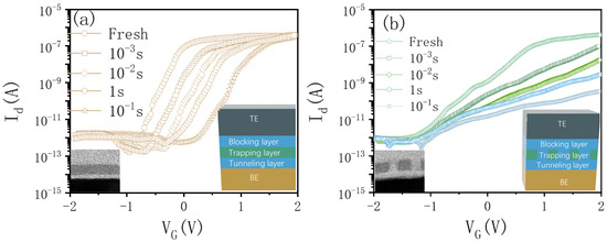
Figure 1.
The transfer characteristics of (a) the control device and (b) the proposed device at different programming times under a voltage of 14 V. The schematic diagrams illustrate the stacked structure of the proposed device (inset, a) and the structure of the control device (inset, b).
In this study, we implemented two different structural designs to explore their effects on charge capture and memory performance. The first is the proposed device, which features a specifically patterned charge-trapping layer. Specifically, we used electron beam lithography (EBL) and inductively coupled plasma (ICP) etching processes to form a rectangular array of 3 μm in length, 30 nanometers in width, and 3 nm in thickness on a silicon substrate. This process ensured the complete separation of the charge-trapping layer at the microscale. This patterned design aims to study the specific impacts of microstructures on charge dynamics and memory windows. In contrast, the control sample utilized an unpatterned, intact charge-trapping layer, maintaining the characteristics of traditional charge-trapping flash memory structures. This design allows us to directly compare the effects of patterning on the electronic properties, thereby more clearly revealing how structural changes contribute to device performance.
In this study, the transfer characteristics of charge trap memory devices were tested by applying a programming voltage of 14 volts for different pulse durations. As illustrated in Figure 1a,b, the performance of both standard (yellow) and our newly developed devices (green) during programming is presented. The transfer curves of both devices shifted positively with the increase in programming time, confirming their normal operational state [11]. A notable difference is observed in the shifting behavior of the curves; the standard device’s characteristics shifted in parallel, whereas our developed device exhibited a dispersed shift, resulting in a larger threshold voltage (Vt) shift under the same current conditions. This new device effectively functions as two parallel transistors: one with a complete core triple-layer structure and another consisting only of an oxide layer on the sidewall [12,13]. During programming, the Vt of the sidewall transistor remains constant, while the Vt of the triple-layer structure transistor increases due to the introduction of the charge trap layer, leading to a non-linear shift in Vt. Our device demonstrated a decline in subthreshold swing (SS) characteristics, which was attributed to differences in structural design. Notably, the significantly enhanced charge injection efficiency in our device allows for a greater accumulation of charges in the charge trap layer and faster injection under the same conditions. However, the incorporation of the separated charge trap layer adversely affected the gate’s control over the channel, a phenomenon further confirmed by subsequent TCAD simulation analyses. The insets in Figure 1 display the optimized triple-layer (OTS) stack structure of our device (a) and its comparison with the standard device (b), where OTS layers refer to the optimized blocking layer (pure HfO2), charge-trapping layer (Ti-doped HfO2), and tunneling layer (Si-doped HfO2). Throughout our experiments, meticulous records were kept of the device’s evolution from a pristine state through up to 10 s of programming, with a particular focus on the gradual increase in threshold voltage over time. Despite a reduction in subthreshold swing performance, our proposed device exhibited significant improvements in programming efficiency and charge retention capability.
Figure 2a,b provide a detailed look at the performance of novel memory devices over a range of programming and erasing conditions, showcasing the impact of different bias voltages on device behavior. The temporal progression of threshold voltage shifts (ΔVt) serves as key indicators of the memory states during programming and erasing operations. Figure 2a focuses on the programming characteristics, where the devices are subjected to incremental programming times under bias voltages of 14 V, 16 V, and 18 V. The plot reveals the efficiency of charge accumulation within the devices—evidenced by the ΔVt—a crucial factor determining the speed of writing data into memory cells. Notably, the devices programmed at higher voltages demonstrate a more pronounced ΔVt, which indicates a more substantial charge trapping within the memory’s dielectric layers. This behavior suggests a strong correlation between the applied voltage and the device’s capability to rapidly transition to a programmed state, a vital attribute for high-speed memory applications. Specifically, Figure 2a captures the programming response across three distinct voltage biases, illustrating that the proposed devices exhibit significantly faster programming speeds compared to the standard control group. The trends observed in threshold voltage shifts further validate the superior performance of our devices under all testing conditions. Similarly, Figure 2b illustrates the erasure characteristics, where the devices are again tested at the same voltage biases but in reverse polarity, facilitating the removal of trapped charges from the dielectric layers. The trend lines for the erasure process mirror the programming phase, yet inversely, with ΔVt decreasing as the erasure time extends, depicting the charge detrapping efficiency. Devices exposed to higher negative bias voltages exhibit a faster decrease in ΔVt, correlating to a quicker erasure time. This rapid erasure capability is pivotal for efficient memory refresh cycles and overall device longevity. The erasure performance of the same devices demonstrates that the new devices also surpass the control devices in erasure speed, which is in line with their programming performance advantages. The graphical representations in these figures are indicative of the fine-tuned control achieved over the memory cells’ charge states in the proposed devices. They demonstrate a clear advancement over the control group with both faster programming and erasing speeds, an outcome of the meticulous engineering of the charge-trapping layers and dielectric materials. These enhancements facilitate not only the acceleration of the P/E cycles but also the precision with which these states are controlled, contributing to the reliability and endurance of the memory device.
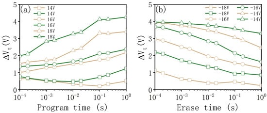
Figure 2.
(a) Programming dynamics of the new design device (green) and the control device (yellow) at multiple voltage levels. (b) Performance of the new design device (green) and the control device (yellow) during the erase process at multiple voltage levels.
Moreover, the swift programming and erasure times are emblematic of the potential for these devices to handle higher data throughput rates, a critical requirement for modern storage solutions catering to the burgeoning demands of data-intensive applications. The improved speed does not come at the expense of device integrity or data retention, as the consistent performance over multiple cycles suggests excellent endurance and stability, which are essential for non-volatile memory applications. In summary, the findings elucidated in Figure 2a,b highlight the advancements in non-volatile memory from the proposed devices for handling rapid programming and erasing operations.
To investigate the charge storage performance of our newly designed device structure, we compared the performance of double-ended capacitors fabricated based on this structure. Utilizing capacitance–voltage (C-V) measurement techniques, Figure 3 reveals the ΔVFB of proposed and control capacitors across varying charge-trapping layer thicknesses. As the thickness of the charge-trapping layer increases, the ΔVFB of both capacitor types rises in tandem. However, at equivalent charge-trapping layer thicknesses, the proposed capacitor demonstrates a wider memory window than the traditional capacitor, suggesting that the proposed device is capable of trapping more charges even at the same physical thickness [14,15]. This phenomenon is likely due to the reduced EOT in the proposed device, which enhances the local electric field across the core layers. Interestingly, as the charge-trapping layer becomes thicker, the ΔVFB of the proposed capacitor exhibits a continuously increasing trend, unlike the control capacitor, which gradually saturates with increased thickness. This indicates the advantage of the proposed capacitor in terms of enhanced local electric fields, especially notable in ultra-thin trapping layers (less than 5 nm) where the memory window of the proposed capacitor significantly exceeds that of the 7 nm-thick charge-trapping layer in the control structure.
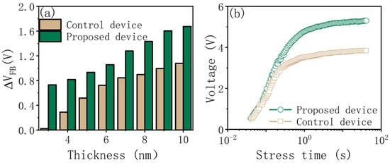
Figure 3.
(a) Relationship between the flat-band voltage shift (ΔVFB) and the thickness of the charge-trapping layer under 1 MHz high-frequency conditions for both developed and control capacitors, and (b) the charge-trapping behavior of both types of capacitors under a constant current stress of 10−8 A.
Furthermore, we assessed the charge-trapping density of both devices using constant current stress tests. Figure 3b showcases the charge-trapping behavior of both capacitors under fixed current stress. The voltage drop across the core layers, measured as a shift in gate voltage over increasing stress time, reflects the charge-trapping efficacy within the charge-trapping layer. The significant change in gate voltage indicates that, compared to the control capacitor, our proposed structure possesses robust charge-trapping capabilities. Therefore, it can be concluded that the separated charge-trapping layer exhibits superior charge-trapping characteristics compared to the traditional intact control charge-trapping layer, even at the same thickness.
As shown in Figure 4a–c, the proposed device structure can be extended into the 3D NAND string. Due to the significant reduction in the effective oxide thickness (EOT) of the high-k dielectric layers, an improved gate-to-channel coupling effect is anticipated. Moreover, the reduction in the physical volume of the charge-trapping layer minimizes noise disturbances caused by the interaction between the charge-trapping layer and adjacent layers [16,17]. As previously mentioned, the notable improvement in the programming and erasing performance of the proposed device mainly results from the substantial reduction in the EOT of the gate dielectric. In our device structure design, the EOT of the gate dielectric has been significantly decreased, leading to a corresponding increase in the electric field, thereby greatly facilitating the charge capture and release processes. Additionally, the proposed device strengthens the internal electric field within the gate dielectric by reducing the EOT and physically encases the charge-trapping layer with high-k dielectric material. The electric field near the corner region, which is significantly stronger than that in the planar bulk region due to the increase in contact area by segmented fabrication, is further enhanced in the proposed device structure, thereby increasing the contact area between the charge-trapping layer and the gate dielectric. As depicted in Figure 4d, the steepening of the energy band distribution inside the tunneling oxide, due to the enhanced electric field, effectively improves the efficiency of charge injection [18,19]. Simultaneously, the all-around coverage of the separated layer by high-k dielectric material ensures no degradation in performance compared to the traditional intact charge-trapping layer, maintaining an acceptable level of charge retention.
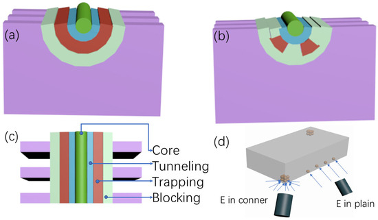
Figure 4.
(a) The charge-trapping layer (indicated in blue) extended in the 3D-NAND string based on the control device, including three types of cell units: center gate (CG) and two side gates (SG). (b) The charge-trapping layer extended in the 3D-NAND string based on the proposed device. (c) Cross section illustration of the 3D-NAND lateral structure. (d) Schematic illustration of the corner field and planar field.
In Figure 5a,b, we are presented with a visual and quantitative analysis of charge retention capabilities for cutting-edge memory structures tested under standard room temperature conditions. These figures graphically represent the retention performance of both the newly developed and traditional control structures over an expansive time scale. The data depicted showcase the average charge decay rates in both programmed and erased states, offering a clear comparison between the endurance of the novel and control structures. Figure 5a shows the programmed state where the novel structure exhibits an average charge decay rate of 134 mV/decade, slightly lower than the control’s 137 mV/decade, indicating a subtle yet impactful enhancement in charge stability over time. Regarding the minimal differences in charge decay rates between the two samples you mentioned (from 134 mV/decade to 137 mV/decade in Figure 5), we agree that the differences are not significant. In the revised manuscript, we have added a more objective evaluation of this observation and provided explanations for it, possibly due to the interaction between interfaces caused by the discontinuous structure relative to the intact structure. In Figure 5b, the erased state further amplifies this contrast, with decay rates of 165 mV/decade for the novel device and 184 mV/decade for the control, underscoring the superior retention characteristics of the new design. What is particularly noteworthy from the extrapolated data is the promising projection that, even after an extended period of 10 years, the memory window of the proposed device is estimated to remain sizeable at 1.25 V. This sustained memory window, a significant indicator of long-term data retention, contrasts with many contemporary memory devices that experience considerable degradation over similar periods. The robustness of the proposed device’s memory window reflects the effectiveness of the advanced materials and structural engineering at play. The proposed device leverages an optimized charge-trapping layer, which not only retains charges with greater efficiency but also injects them more effectively during the programming phase. This dual capability is a substantial leap forward in memory technology, where the trade-off between charge injection and retention has often been a limiting factor. The enhanced charge injection mechanism ensures that the initial memory state is set with higher precision and the final state remains stable, surpassing the control sample in both aspects. These characteristics suggest that the novel device structure can significantly improve the performance and reliability of flash memories, where the demand for high-endurance storage solutions continues to escalate. Furthermore, the presented data in Figure 5a,b speak volumes about the inherent stability of the novel structure. They stand as a testament to the durability of the device, showing no detectable endurance degradation after 105 programming/erasing cycles.
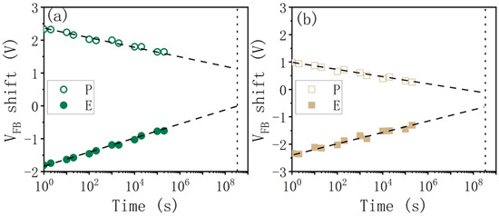
Figure 5.
Retention characteristics of both the proposed (a) and control (b) structures measured at room temperature.
Figure 6a reveals the endurance characteristics of the two devices, showing no noticeable endurance degradation even after 105 programming/erasing cycles, indicating the proposed device’s suitability for flash memory applications. This stability underscores a key advantage of the proposed structure: enhancing charge injection efficiency without compromising charge retention. The dilemma between charge injection and retention has long been identified as a primary challenge for floating gate memories, including nanocrystal floating gates [19,20]. Given the simplicity of our proposed separated structure, this finding is notably intriguing and holds practical significance, with further investigations currently underway. TCAD simulations have depicted the cross-sectional electric field of the proposed device, as shown in Figure 6b. These simulations validated an improvement in the charge injection efficiency of the new device, thereby ensuring rapid programming/erasing performance. The vertical electric field within the tunneling oxide is notably intensified in the “corner” areas of the proposed structure. This enhancement of the electric field is likely due to a combination of specific local corner geometries and reduced EOT. Furthermore, the strong local field also facilitates thermal electrons to enter the charge-trapping layer, not only via Fowler–Nordheim (FN) tunneling but also directly [20].
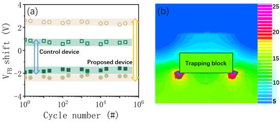
Figure 6.
(a) Long-term stability between the novel structure and the traditional control structure. (b) Cross-sectional view of the electric field distribution within the core layers, as derived from TCAD simulations.
Figure 6 showcases the resilience and effectiveness of our advanced device architecture in sustaining memory integrity over extensive use. Panel (a) visually captures the endurance characteristics of both the traditional and the innovative devices, with an outstanding lack of endurance degradation after more than 100,000 program/erase (P/E) cycles. Such robustness is emblematic of the proposed device’s excellence for contemporary flash memory applications, aligning with the most rigorous of industry standards. This remarkable stability elucidates a salient advantage of our proposed structure: it manages to augment charge injection efficiency while concurrently ensuring the preservation of charge retention capabilities. Historically, this juxtaposition between charge injection and retention has posed a significant hurdle for the efficacy of floating gate memories, including those employing nanocrystal floating gates. Extensive research provides a rich context to this discourse, with the innovative approach presented here offering a promising resolution. Our separated structure’s simplicity is not only intriguing in its conceptual clarity but also in its substantial application potential, marking a pivotal step forward in-memory technology. Current investigations continue to delve into the nuanced advantages and potential expansions of this design. The cross-sectional electric field analysis facilitated by TCAD simulations, as portrayed in Figure 6b, underscores a substantial improvement in the charge injection efficiency within our device. These simulations demonstrate that the vertical electric field within the tunneling oxide layer is significantly amplified at the structure’s corner regions, enhancing the local electric fields. This phenomenon likely results from a synergistic effect of the particular geometric configurations at these corners and the strategic reduction in effective oxide thickness (EOT).
Moreover, the simulations indicate that this increased electric field strength contributes not only to Fowler–Nordheim (FN) tunneling but also to the direct entry of thermal electrons into the charge-trapping layer. This mechanism holds considerable implications for the memory’s performance, offering a dual pathway for charge movement that could lead to breakthroughs in the speed and reliability of future storage devices. In addition, our study explores the correlation between the structural attributes of the trapping layer and the overall memory performance. It suggests that the sophisticated design of the trapping block significantly contributes to the device’s efficiency. The trapping block, tailored with meticulous precision, aligns with the high-k dielectric parameters to furnish a conducive environment for charge retention and injection, marrying the best of material science with innovative engineering. Our research presents an elaborate discussion on the trapping block’s role in memory window expansion. The block’s architecture, combined with the electric field enhancement, results in a more extensive memory window, indicating a larger capacity for charge storage and retention over extended periods. This window not only signifies the device’s immediate efficacy but also its long-term reliability, a critical factor in the longevity of memory storage applications. This comprehensive analysis, covering a span of operational cycles, suggests that the proposed device’s memory window would remain significantly large even after a decade, standing at an estimated 1.25 V. The lack of degradation over time, as evidenced by the flat-band voltage shifts, asserts the device’s enduring quality, marking a substantial improvement over traditional designs with intact charge-trapping layers. The initial and final window sizes of our sample surpass those of the control, underlining the efficiency of our charge injection process. The findings from Figure 6a,b coalesce to affirm the formidable charge-trapping ability of our structure compared to the control. The charge trapping characteristics, gleaned from constant current stress measurements, highlight the proposed device’s superior charge trapping density. Even at comparable thicknesses, our separated charge-trapping layer outperforms the intact control layer, a testament to the advanced charge-trapping mechanism employed in our design.
In our study, we employed an optimized tunnel structure (OTS) design, incorporating titanium (Ti) doping in the charge-trapping layer and using silicon-doped hafnium oxide (HfO2) as the tunneling layer, which significantly enhanced the performance of the charge-trapping flash memory (CTF). This doping not only altered the physical and chemical properties of these materials but also profoundly impacted their electrical properties, optimizing the functionality of the entire storage device.
The introduction of titanium adjusted the conduction band edge of HfO2, reducing band misalignment with the silicon substrate, thereby effectively minimizing unintended electron leakage. This alteration enhanced the efficiency of electron injection, allowing for effective charge injection at lower voltages. Additionally, the increase in defect states caused by doping served as temporary traps for charges, helping to store more charges in the charge-trapping layer and improving storage efficiency. The incorporation of silicon significantly improved the physical properties of HfO2, reducing the effective oxide thickness (EOT) and increasing the dielectric constant of the tunneling layer. These physical changes not only lowered the tunneling barrier for electrons from the substrate to the charge-trapping layer but also enhanced the stability of electrons within the charge layer, thereby boosting charge injection efficiency. Furthermore, the silicon-doped HfO2 layer, due to its excellent chemical stability and dielectric properties, effectively suppressed unwanted charge leakage toward the substrate or gate, and its reduced sensitivity to environmental factors such as temperature and humidity further enhanced the device’s reliability and durability.
The Coulomb blockade effect, observed in nano-scale quantum dot structures, occurs when electron numbers are restricted, and the Coulomb repulsion among electrons impedes the system’s conductivity. In our design, we utilized nano-scale boundary and corner structures within the charge-trapping layer, leveraging the Coulomb blockade effect to control the flow of charges. As the charge layer becomes saturated due to electron injection, the entry of additional electrons becomes challenging because they must overcome the additional energy produced by interactions among charges. The Coulomb blockade effect ensures that charges are not easily lost due to thermal activation, significantly enhancing the long-term retention of charges. This design not only allows our charge-trapping layer to capture charges efficiently but also maintains charge stability without the need for high voltages. The structure not only speeds up programming and erasing but also effectively reduces charge leakage, extending the data retention time of the device. Experimental results show that the improved CTF devices, with the same thickness of the charge-trapping layer, exhibit a larger memory window and superior charge retention capability.
In conclusion, this study explores the charge-trapping characteristics of separated charge-trapping layers. The newly proposed structure demonstrates a significantly broader memory window under the same test conditions compared to conventional storage technologies. This groundbreaking improvement is attributed to the effective reduction of the effective oxide thickness (EOT) of the gate dielectric, thereby enhancing the local electric field within the tunneling oxide layer and significantly increasing the efficiency of charge injection. Achieving a substantial enhancement in programming and erasing characteristics at low operating voltages suggests the immense potential of the novel charge-trapping flash memory technology for future high-performance storage devices. This in-depth research provides valuable insights into the charge-trapping characteristics of separated layers. It emphasizes the expansive memory window exhibited by our proposed structure under identical testing conditions, attributed to the strategic reduction in EOT, which fortifies the local electric fields within the oxide layers, thereby refining charge injection. The enhanced program/erase characteristics, achieved at low operating voltages and high speeds, spotlight the tremendous potential of new charge trap flash memory technology for next-generation high-performance storage devices.
Author Contributions
Investigation, K.W., J.L., Z.X., Z.W. and H.J.; Data curation, R.L.; Funding acquisition, R.J. All authors have read and agreed to the published version of the manuscript.
Funding
It is sponsored by the Natural Science Foundation of Ningbo Municipality (2023J007), the Natural Sciences Fund of Zhejiang Province (LDT23F05015F05). This work was also supported by the Opening Project of Key Laboratory of Microelectronic Devices & Integrated Technology Institute of Microelectronics, Chinese Academy of Sciences.
Data Availability Statement
Data is contained within the article.
Conflicts of Interest
The authors declare no conflict of interest.
References
- Cho, S. Fast memory and storage architectures for the big data era. In Proceedings of the 2015 IEEE Asian Solid-State Circuits Conference (A-SSCC), Xiamen, China, 9–11 November 2015; pp. 1–4. [Google Scholar]
- Lee, M.C.; Wong, H.Y. Threshold voltage instability mechanisms of nitride based charge trap flash memory—A review. J. Nanosci. Nanotechnol. 2014, 14, 4799–4812. [Google Scholar] [CrossRef] [PubMed]
- Goto, T.; Suwa, T.; Katayama, K.; Nishida, S.; Ikenoue, H.; Sugawa, S. Threshold voltage uniformity improvement by introducing charge injection tuning for low-temperature poly-Si thin film transistors with metal/oxide/nitride/oxide/silicon structure. Jpn. J. Appl. Phys. 2024, 63, 02SP51. [Google Scholar] [CrossRef]
- Sharma, U.; Kumar, G.; Mishra, S.; Thomas, R. Advancement of gate oxides from SiO2 to high-k dielectrics in microprocessor and memory. J. Phys. Conf. Ser. 2022, 2267, 012142. [Google Scholar] [CrossRef]
- Huff, H.R.; Brown, A.; Larson, L.A.; Claeys, C.; Gonzalez, F.; Murota, J.; Saraswat, K. The gate stack/shallow junction challenges for sub-100 nm technology generations. In ULSI Process Integration II; The Electrochemical Society Meeting: Philadelphia, PA, USA, 2001; pp. 223–249. [Google Scholar]
- Tsai, S.-J.; Wang, C.L.; Lee, H.C.; Lin, C.Y.; Chen, J.W.; Shiu, H.W.; Chang, L.Y.; Hsueh, H.T.; Chen, H.Y.; Tsai, J.Y.; et al. Approaching defect-free amorphous silicon nitride by plasma-assisted atomic beam deposition for high performance gate dielectric. Sci. Rep. 2016, 6, 28326. [Google Scholar] [CrossRef] [PubMed]
- Spassov, D.; Paskaleva, A.; Guziewicz, E.; Wozniak, W.; Stanchev, T.; Ivanov, T.; Wojewoda-Budka, J.; Janusz-Skuza, M. Charge storage and reliability characteristics of nonvolatile memory capacitors with HfO2/Al2O3-based charge trapping layers. Materials 2022, 15, 6285. [Google Scholar] [CrossRef] [PubMed]
- Aleiner, I.L.; Brouwer, P.W.; Glazman, L.I. Quantum effects in Coulomb blockade. Phys. Rep. 2002, 358, 309–440. [Google Scholar] [CrossRef]
- Kavokine, N.; Marbach, S.; Siria, A.; Bocquet, L. Ionic Coulomb blockade as a fractional Wien effect. Nat. Nanotechnol. 2019, 14, 573–578. [Google Scholar] [CrossRef] [PubMed]
- Chang, T.-C.; Jian, F.-Y.; Chen, S.-C.; Tsai, Y.-T. Developments in nanocrystal memory. Mater. Today 2011, 14, 608–615. [Google Scholar] [CrossRef]
- Kim, S.-J.; Lee, J.-S. Flexible organic transistor memory devices. Nano Lett. 2010, 10, 2884–2890. [Google Scholar] [CrossRef] [PubMed]
- Zhang, Z.; Wang, Z.; Shi, T.; Bi, C.; Rao, F.; Cai, Y.; Liu, Q.; Wu, H.; Zhou, P. Memory materials and devices: From concept to application. InfoMat 2020, 2, 261–290. [Google Scholar] [CrossRef]
- Oh, H.; Kim, J.Y.; Kim, J.H.; Park, S.G.; Kim, D.H.; Kim, S.E.; Woo, D.S.; Lee, Y.S.; Ha, G.W.; Park, J.M.; et al. High-density low-power-operating DRAM device adopting 6F/sup 2/cell scheme with novel S-RCAT structure on 80 nm feature size and beyond. In Proceedings of the 35th European Solid-State Device Research Conference, ESSDERC, Grenoble, France, 16 September 2005; pp. 177–180. [Google Scholar]
- Meena, J.S.; Sze, S.M.; Chand, U.; Tseng, T.-Y. Overview of emerging nonvolatile memory technologies. Nanoscale Res. Lett. 2014, 9, 1–33. [Google Scholar] [CrossRef] [PubMed]
- Chen, H.; Zhou, Y.; Han, S.T. Recent advances in metal nanoparticle-based floating gate memory. Nano Sel. 2021, 2, 1245–1265. [Google Scholar] [CrossRef]
- Kim, S.S.; Yong, S.K.; Kim, W.; Kang, S.; Park, H.W.; Yoon, K.J.; Sheen, D.S.; Lee, S.; Hwang, C.S. Review of semiconductor flash memory devices for material and process issues. Adv. Mater. 2023, 35, 2200659. [Google Scholar] [CrossRef] [PubMed]
- Goda, A. 3-D NAND technology achievements and future scaling perspectives. IEEE Trans. Electron Devices 2020, 67, 1373–1381. [Google Scholar] [CrossRef]
- Faccio, F.; Borghello, G.; Lerario, E.; Fleetwood, D.M.; Schrimpf, R.D.; Gong, H.; Zhang, E.X.; Wang, P.; Michelis, S.; Gerardin, S.; et al. Influence of LDD spacers and H+ transport on the total-ionizing-dose response of 65-nm MOSFETs irradiated to ultrahigh doses. IEEE Trans. Nucl. Sci. 2017, 65, 164–174. [Google Scholar] [CrossRef]
- Beneventi, G.B.; Gnani, E.; Gnudi, A.; Reggiani, S.; Baccarani, G. Dual-metal-gate InAs tunnel FET with enhanced turn-on steepness and high on-current. IEEE Trans. Electron Devices 2014, 61, 776–784. [Google Scholar] [CrossRef]
- Banerjee, W.; Kashir, A.; Kamba, S. Hafnium oxide (HfO2)—A multifunctional oxide: A review on the prospect and challenges of hafnium oxide in resistive switching and ferroelectric memories. Small 2022, 18, 2107575. [Google Scholar] [CrossRef] [PubMed]
Disclaimer/Publisher’s Note: The statements, opinions and data contained in all publications are solely those of the individual author(s) and contributor(s) and not of MDPI and/or the editor(s). MDPI and/or the editor(s) disclaim responsibility for any injury to people or property resulting from any ideas, methods, instructions or products referred to in the content. |
© 2024 by the authors. Licensee MDPI, Basel, Switzerland. This article is an open access article distributed under the terms and conditions of the Creative Commons Attribution (CC BY) license (https://creativecommons.org/licenses/by/4.0/).