Abstract
The issue of sub-module (SM) capacitor voltage unbalance is a hot topic in the current research into the modular multilevel converter (MMC). An excellent strategy comprises mitigating the SM capacitor voltage imbalance by adjusting the SM on time. The traditional capacitor voltage balancing control regulates the speed to maintain accuracy. A unique SM capacitor voltage balancing control strategy is presented in this paper and is based on conventional capacitor voltage balance management and neural network prediction. Firstly, the SM capacitor voltage and arm current are speculated by operating the time series forecasting technique in real time, considering the dynamic changes in the SM capacitor voltage and arm current. Secondly, the SM capacitor voltage distinction between the actual and theoretical value is determined, and a deviation’s mixed Gaussian distribution is established to estimate its compensation voltage. Thirdly, the SM triggering sequence is anticipated by using the neural network along with the pilot values of the SM capacitor voltage, arm current, and the offset compensation value, and the control is executed. Finally, a three-phase, six-leg, eight-module, nine-level MMC model is built to verify the feasibility of the suggested approach.
1. Introduction
The modular multilevel converter (MMC) represents the most recent iteration of voltage source converters. When operated, the converter’s active and reactive power, voltage, and current can be modified independently, providing minimal loss and high-quality output voltage waveforms [1,2,3,4]. However, due to the diverse capacitor values of each sub-module (SM), the SM capacitor voltage deviates from the theoretical voltage during the inverter process, resulting in the SM capacitor voltage imbalance, leading to upper- and lower-bridge voltage fluctuations, increasing the circulating current between the bridges and reducing the DC voltage utilization.
As a result, a switching function model was used to analyze the coupling relationship between the SM electrical quantities [5] and the steady-state characteristics of the SM electrical quantities and design the main circuit’s parameters. Meanwhile, according to the MMC structure, the bridge arm’s instantaneous power equation was established [6] and revealed the existence of the second-harmonic component in the circulating current. According to the components of the circulating current, a generalized controller-based circulating current suppression strategy [7,8], reactive circulating current injection [9], is proposed, which incorporates the CPS-PWM modulation method to achieve the SM output voltage balancing, but increases the SM’s switching frequency and loss. A guiding factor [10] and a balancing regulation index [11] are introduced to achieve a flexible trade-off between switching frequency and capacitor voltage balancing. At the same time, the disadvantages of the CPS-PWM modulation method are fully demonstrated and the use of carrier cascading is proposed, but the rotation period of the carriers will have an extremely important effect on the control. In addition, when carrier modulation is used, it is necessary to establish an independent capacitor voltage control circuit for each SM, which increases the cost of the control link. Moreover, the extraction of the circulation component will directly affect the SM capacitor voltage balancing control, which improves the complexity of the control link.
The modulation method using nearest level approximation [12,13] is proposed to accomplish balanced control of SM capacitor voltages by conducting bubble sort [14], base sort [15], group sort [16], and subsumption sort [17] on the capacitor voltages, which reduces the effect of the output due to capacitor parameter differences. However, as the SM number increases, the computer’s performance is required to be higher. It is not conducive to rapidly adjusting active and reactive power, voltage, and current.
All the above capacitor voltage balancing control strategies need to use specialized sensors, leading to a cost increase for capacitor voltage balancing control. For this purpose, Kalman filtering [18], state observer [19], and the online estimation of arm currents [20] are implemented to predict the arm currents. In addition, SM capacitor voltage balancing has been achieved by changing the SM topology, for instance, by adding diodes between neighboring SMs to form a self-homogenizing circuit [21,22,23]. The dynamic balancing of SM capacitor voltages is achieved by introducing flying capacitor multilevel (FCML) converters between adjacent SMs [24]. However, this increases the complexity of the SM topology and is not conducive to later expansion. Further, the SM capacitor voltage output interval was partitioned using a field-programmable gate array (FPGA) to achieve SM capacitor voltage dynamic balancing [25,26], improving its balancing control speed. Nevertheless, the interval division and the number setting of intervals will seriously affect the balancing control effect. If SMs were placed in the same output interval, the capacitor voltage balancing control would not be any better. The active and reactive power, voltage, and current could not be precisely controlled.
In practical engineering, it is necessary to regulate the speed at the cost when utilizing the above methods to satisfy the control accuracy. For this reason, using the traditional capacitor voltage balancing control strategy, the SM capacitor voltage, turn-on sequence, and arm current are regarded as the initial data. The MMC input and output parameters’ fluctuation interval is divided into smaller segments. The SM capacitor voltage and arm current will evolve when the input and output parameters change. Consequently, the primary database is updated and supplemented. An SM capacitor voltage balancing control strategy based on neural network forecasting is proposed. Firstly, the SM capacitor voltage and arm current trends and periodicity are analyzed and tested. The time series method is used to predict the SM capacitor voltage and arm current in real time. Secondly, the SM capacitor voltage discrepancy between the actual and theoretical value is estimated, and its mean and variance are generated. We observe the deviation distribution, construct a mixed Gaussian distribution of the voltage offset, and evaluate the compensation value of the voltage offset. Thirdly, taking into account the historical data for the SM capacitor voltage and conduction sequence, the neural network is trained. Considering the predicted SM capacitor voltage, arm current, and deflection compensation value, the SM conduction sequence is predicted and the control is completed. Finally, a simulation model is developed to verify the feasibility of the proposed scheme.
2. Theoretical Analysis
During MMC operation, the SM capacitor parameters are not identical, which constitutes a primary factor in the SM output voltage imbalance. The SM capacitor voltage imbalance is a natural occurrence because of the disparity between the predicted time and the actual on-state time calculated via the modulation.
2.1. SM Capacitor Value Differences
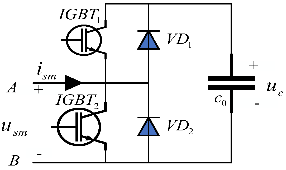
MMC’s basic unit is SM. Its standard structures include the half-bridge type and full-bridge type. In engineering, a half-bridge SM is commonly employed, consisting of two insulated gate bipolar transistors (IGBTs) and a capacitor, as demonstrated in Figure 1.
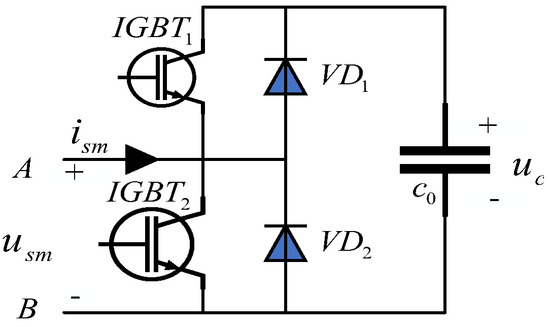
Figure 1.
Basic structure of half-bridge SM.
IGBT1 and IGBT2 determine the SM capacitor C0 charge or discharge. Assuming that ism is active from A to B and vice versa, if the potential of A is higher than that of B, then usm is active and vice versa. The values ‘1’ and ‘0’ indicate IGBT conduction and shutdown, respectively. Then, the relationship between the on–off of IGBT1 and IGBT2, and the state of the SM capacitor C0 is shown in Table 1.

Table 1.
Relationship between the on–off of IGBT1 and IGBT2 and the state of the SM capacitor C0.
From Figure 1, we can see that if the SM initial voltage is u0, then the capacitor voltage uc, instantaneous power pc, and stored energy Wc meet the following relationship during a charging cycle:
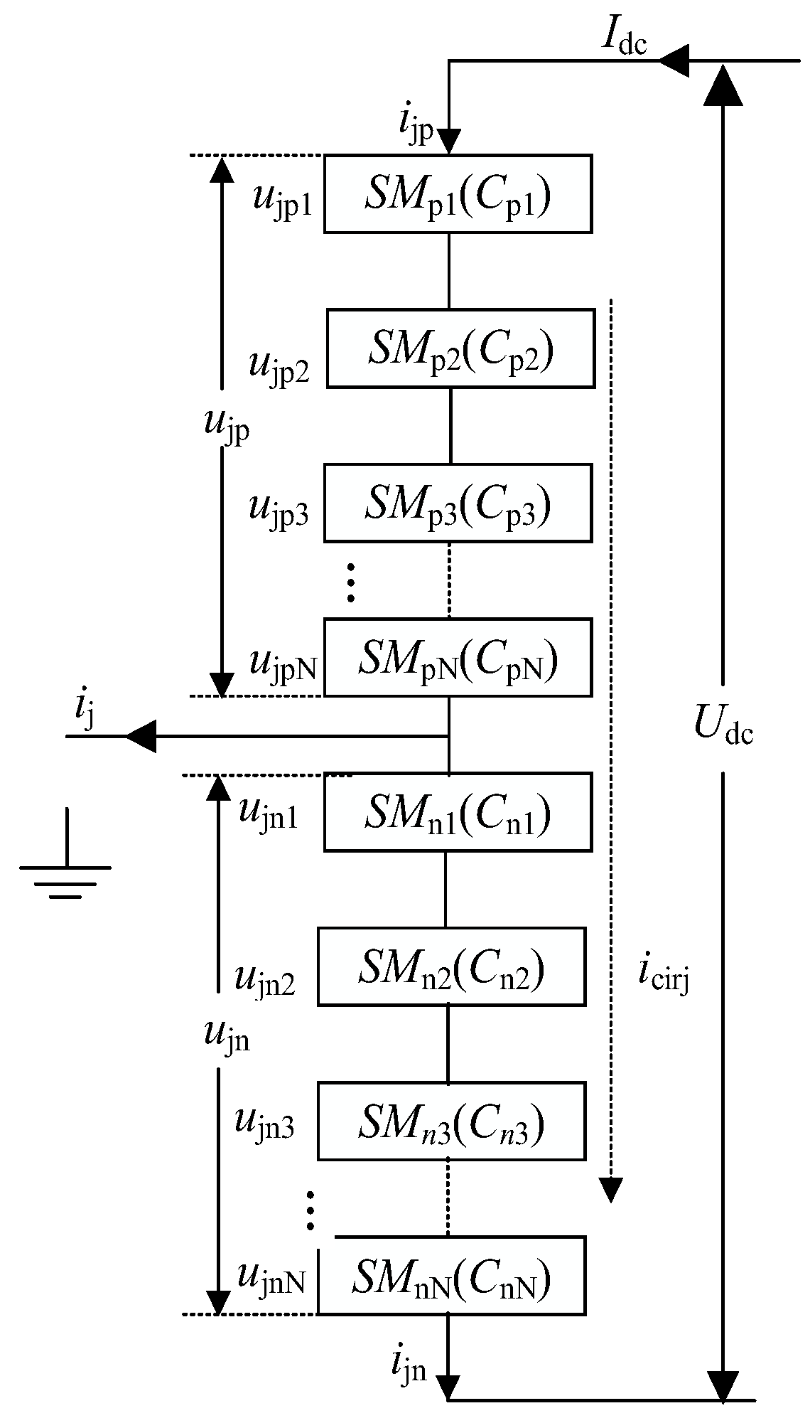
During operation, we suppose that the voltage and current are Udc, Idc at the DC side bus. In phase j(j = a, b, c), the upper arm current is ijp; the number of on-state SMs is npj; and the capacitor value, voltage, and stored energy of the i-th conducting SM are Cpi, ujpi, and Wjpi, respectively. We draw the circuit diagram of phase j, as shown in Figure 2.

Figure 2.
Circuit for phase j.
From Figure 2, we can see that the upper bridge j-phase capacitor voltage ujp and the stored energy Wjp are
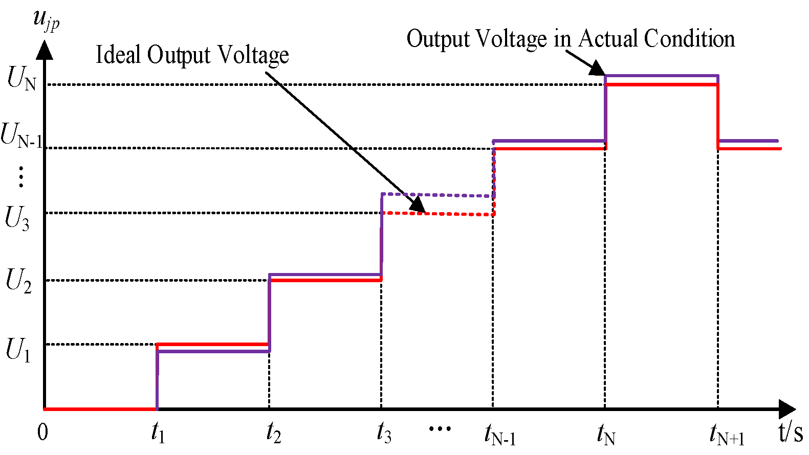
Similarly, according to Equations (4) and (5), the lower-bridge j-th phase capacitor voltage ujn, and capacitor stored energy Wjn are received. If the SM initial voltages are all the same, at the ti moment, SMpi conducts, and the upper-bridge output voltage is Ui, and its variation is Ui − Ui−1 and remains constant. Taking a charge cycle of SMp1 as an example, the upper bridge j-phase output voltage ujp varies, as shown in Table 2.
Table 2.
The turn-on relationship between the output voltage ujp and SM in the upper-bridge j-phase.
Ideally, the SM capacitor values are equal and SMpi conducts according to Table 2, making the voltage changes Ui − Ui−1 similar. In practice, due to capacitor production error or degradation, the SM capacitor values are not identical [27]. Suppose SMpi is turned on according to Table 2. In that case, the actual value for the SMpi capacitor voltage deviates from the theoretical value, which causes the difference between the real value of the output voltage ujp and the theoretical value, resulting in the voltage changes Ui − Ui−1 being dissimilar to the upper-bridge j-phase output voltage ujp, as shown in Figure 3.

Figure 3.
The variation in the output voltage ujp on the j-th phase upper-bridge arm.
Similarly, if the lower-bridge SM capacitor values are not similar, then they cause discrepancies between the actual and theoretical values for the lower-bridge j-phase output voltage ujn.
The circulating current icirj in phase j is
Combining Equations (7) and (8), ijp and ijn are displayed:
The output voltage uj in phase j is
If the SM capacitor values are not the same, then the actual value uj deviates from the theoretical value, exacerbating uj fluctuations.
If Uj is the j-th phase output voltage uj fundamental voltage rms value on the AC side, then the output voltage modulation index m is
Then, the voltage utilization rate n is
In operation, assuming , , then the output instantaneous power pout in phase j is
In phase j, the interphase circulating current icirj is
Substituting Equation (12) into (15) yields
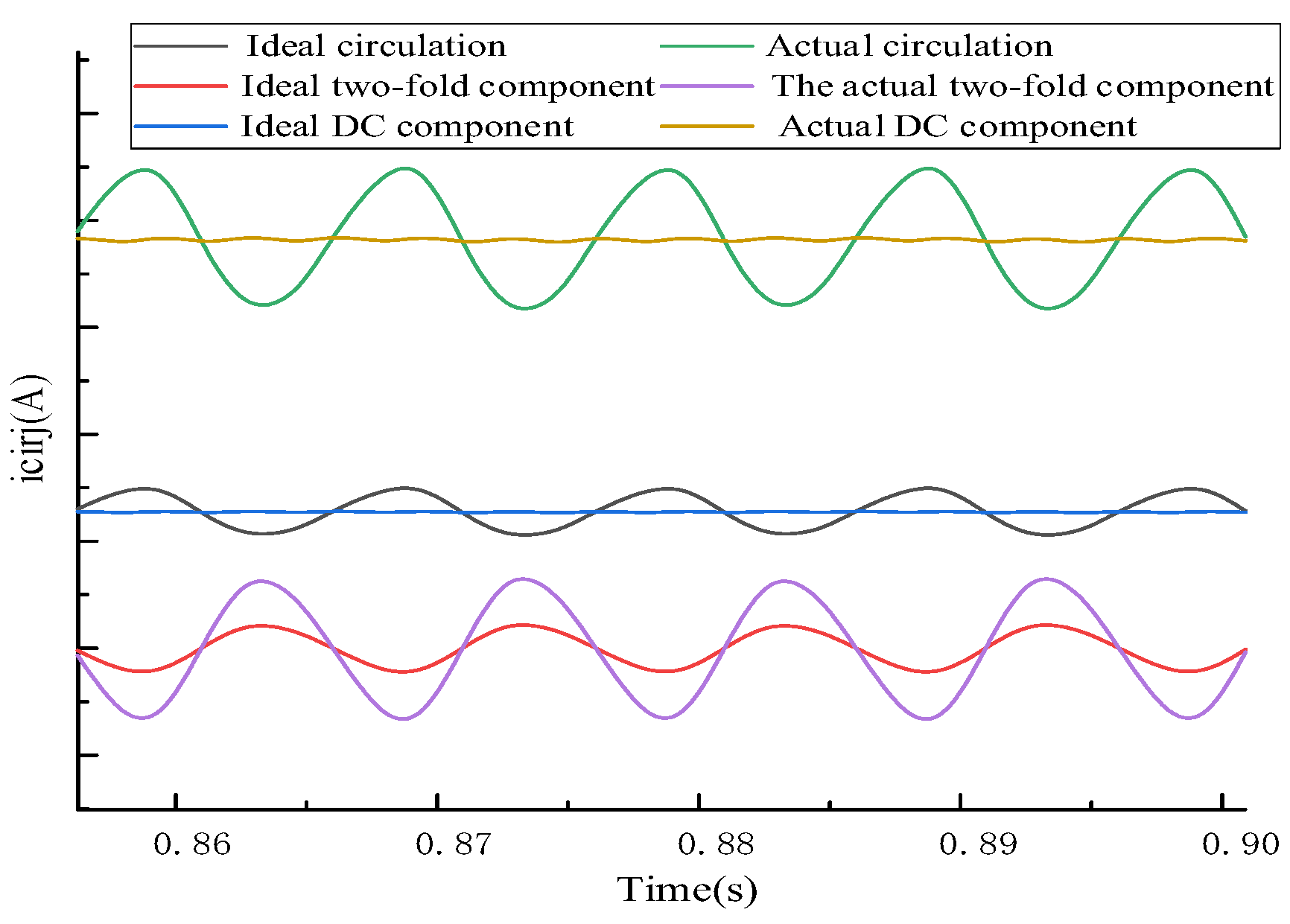
When the SM capacitor Ci is not equal, meaning that the equivalent capacitance decreases in each bridge, causing Idc to increase, the circulating current icirj in the j-th phase is shown in Figure 4.
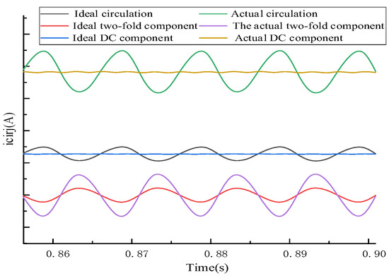
Figure 4.
Circulating current icirj in phase j.
From Figure 4, we can see that the SM capacitor Ci is not the same, causing the circulating current icirj in the actual case to be larger than in the ideal case, making the output voltage modulation ratio m and the DC voltage utilization n smaller than in the ideal case.
2.2. Modulation Scheme
Currently, there are two main modulation methods for MMC: carrier pulse width and step-wave modulation. The carrier pulse width mainly compares the voltage-modulating waveform generated by the vector control link with the triangular carrier waveform to yield a modulating signal and perform the MMC triggering.
Nearest-level modulation (NLM) is commonly employed as step-wave modulation. According to the MMC’s control target, the voltage-modulated waveform is generated by using the vector control method; the number of SMs to be conducted in the upper and lower bridges is counted in real time so that the output voltage on the AC side comes close to the modulating waveform, which is often applied in flexible DC transmission projects because of its simple design, fast response, and wide range of applications. The NLM modulation diagram is shown in Figure 5.
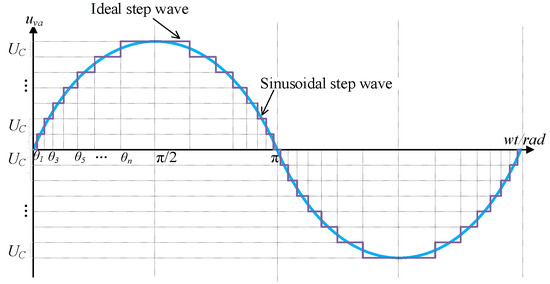
Figure 5.
NLM modulation diagram.
From Figure 5, we can see that the step wave varies with the sinusoidal modulated wave and gradually approaches it. Each arm contains N SMs. Each SM has a capacitor value and voltage of C0 and UC, respectively. For phase j, the number of conductive SMs in the upper- and lower-bridge arms are npj and nnj, separately. According to the modulation strategy, the number of conductive SMs n in each bridge meets 0 ≤ n ≤ N. Then, npj, nnj, satisfy the following relation:
Combined with Equation (6), the ideal value of the SM capacitor voltage UC is
Whenever the NLM is used, the number of SMs on the upper and lower arms are
denotes the ideal modulating wave in the j-th phase at t time.
The SM capacitor voltage is positively related to its stored energy according to the bridge SM connection. We define the discharge rate Ki of the SMi(i = 1, 2, 3…) as
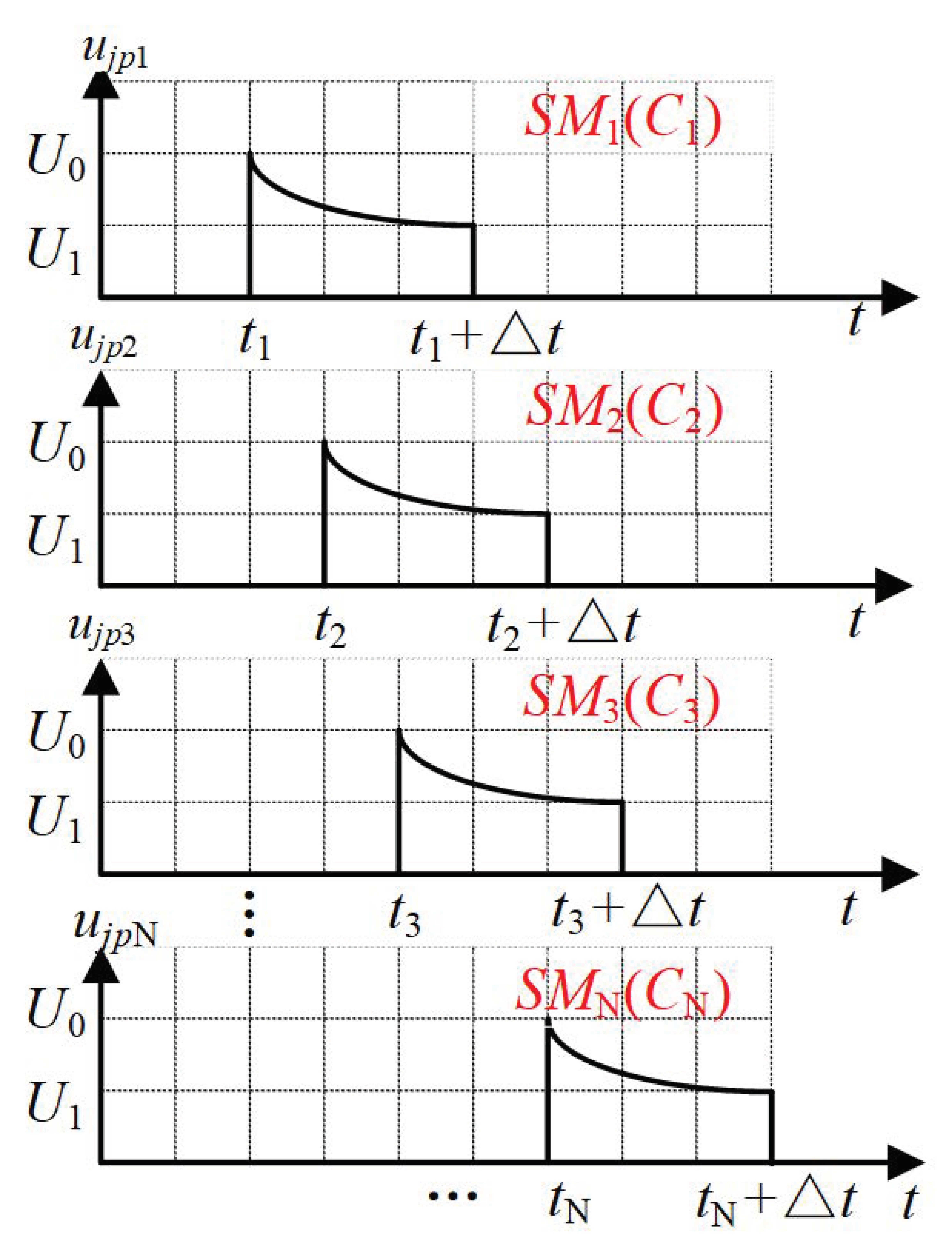
U1i and U0i represent the SMi(i = 1, 2, 3…) capacitor voltage Ui after conduction and before the on-time, respectively; t1i and t0i indicate the SMi(i = 1, 2, 3…) after the on-time and the time before conduction, separately. For example, an MMC requires SMi(i = 1, 2, 3…N) to conduct at t0 moment, and the SM voltage is U0 before it is on. According to the modulation principle of the NLM, the on-time is △t. Then, ideally, the SMi(i = 1, 2, 3…N) discharge diagram is shown in Figure 6.

Figure 6.
Ideally, the SMi(i = 1, 2, 3…N) discharges schematically.
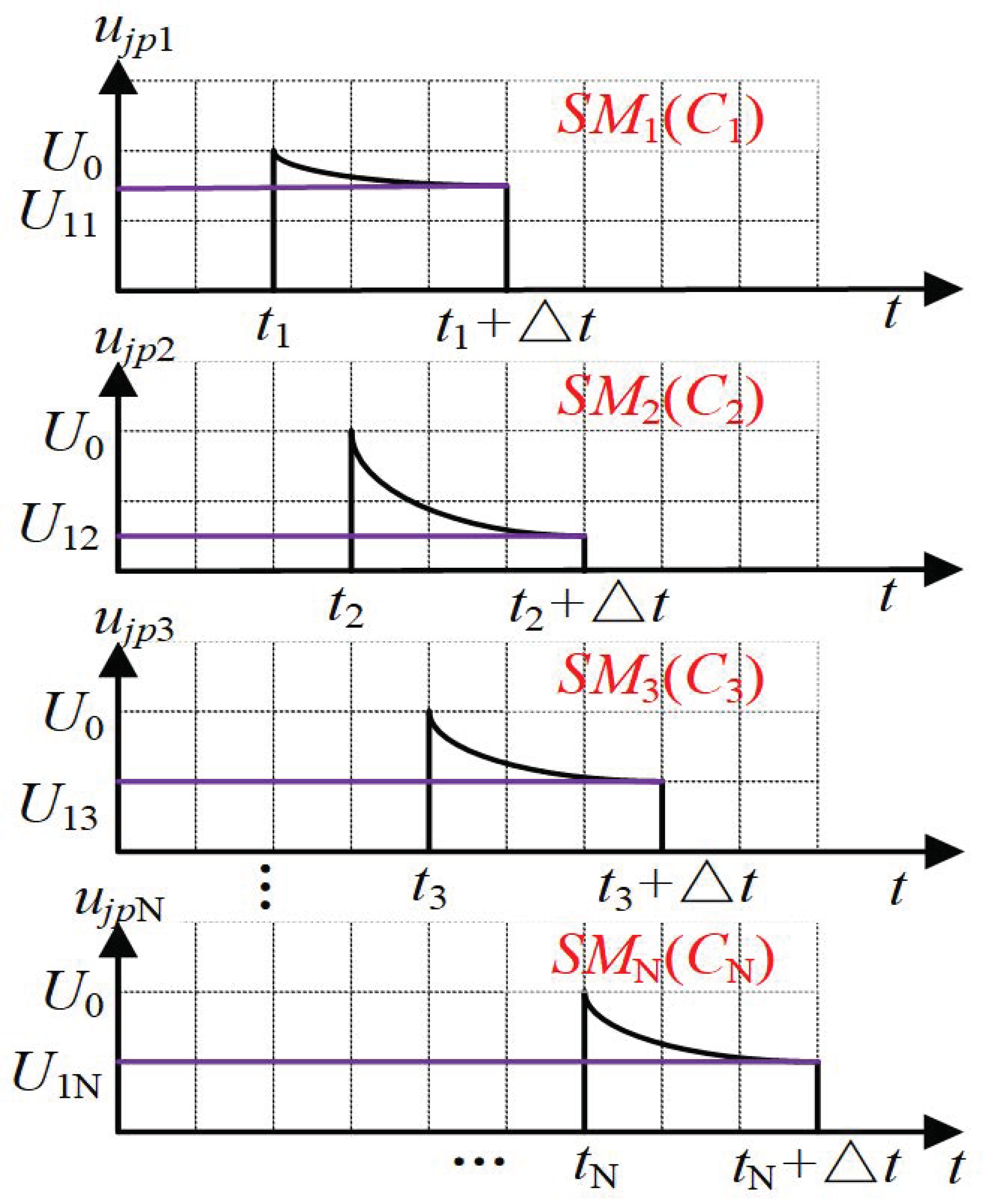
As seen in Figure 6, ideally, C1 = C2 = C3 = …= CN causes the SMi(i = 1, 2, 3…N) to have a matching discharge rate to K. After modulation, the SMi(i = 1, 2, 3…N) still maintains equal capacitor voltage, the same discharge power, and balanced stored energy. However, in actual engineering, the SM capacitor values are not exactly alike; for example, C1 ≠ C2 ≠ C3 = … = CN. At this time, according to the theoretical on-time△t, the actual SMi(i = 1, 2, 3…N) discharge schematic is shown in Figure 7.

Figure 7.
The SMi(i = 1, 2, 3…N) discharge schematic diagram for the actual case.
Comparing Figure 6 and Figure 7, C1 ≠ C2 ≠ C3 = … = CN causes the SMi(i = 1, 2, 3…N) discharge rate K1 < K3 = …KN < K2 in practice. If the SMi(i = 1, 2, 3…N) is discharged according to the theoretically figured on-time △t, making the SMi(i = 1, 2, 3…N) capacitor voltage U1i(i = 1, 2, 3…N), then the discharging power P1i and the stored energy W1i are not exactly alike after the on-time, triggering the SM2 to over-discharge and vibrate. Similarly, if the SMi(i = 1, 2, 3…N) is charged according to the theoretically reckoned on-time, it will induce some SMs to store energy excessively.
In engineering, the SM capacitor values C1 ≠ C2 ≠ C3 ≠ … ≠ CN prompt the SMi(i = 1, 2, 3…N) to charge and discharge at entirely different rates Ki. The SMi(i = 1, 2, 3…N) on-time theoretical time △t1i differs from the conduction △ti calculated by the NLM modulation strategy. After modulation, the SM capacitor voltage deviates from the theoretical value, resulting in unequal energy stored in the different SM capacitors, inducing some SMs to be overcharged and discharged, and reducing the SMs’ service life.
3. Traditional SM Capacitor Voltage Balancing Control
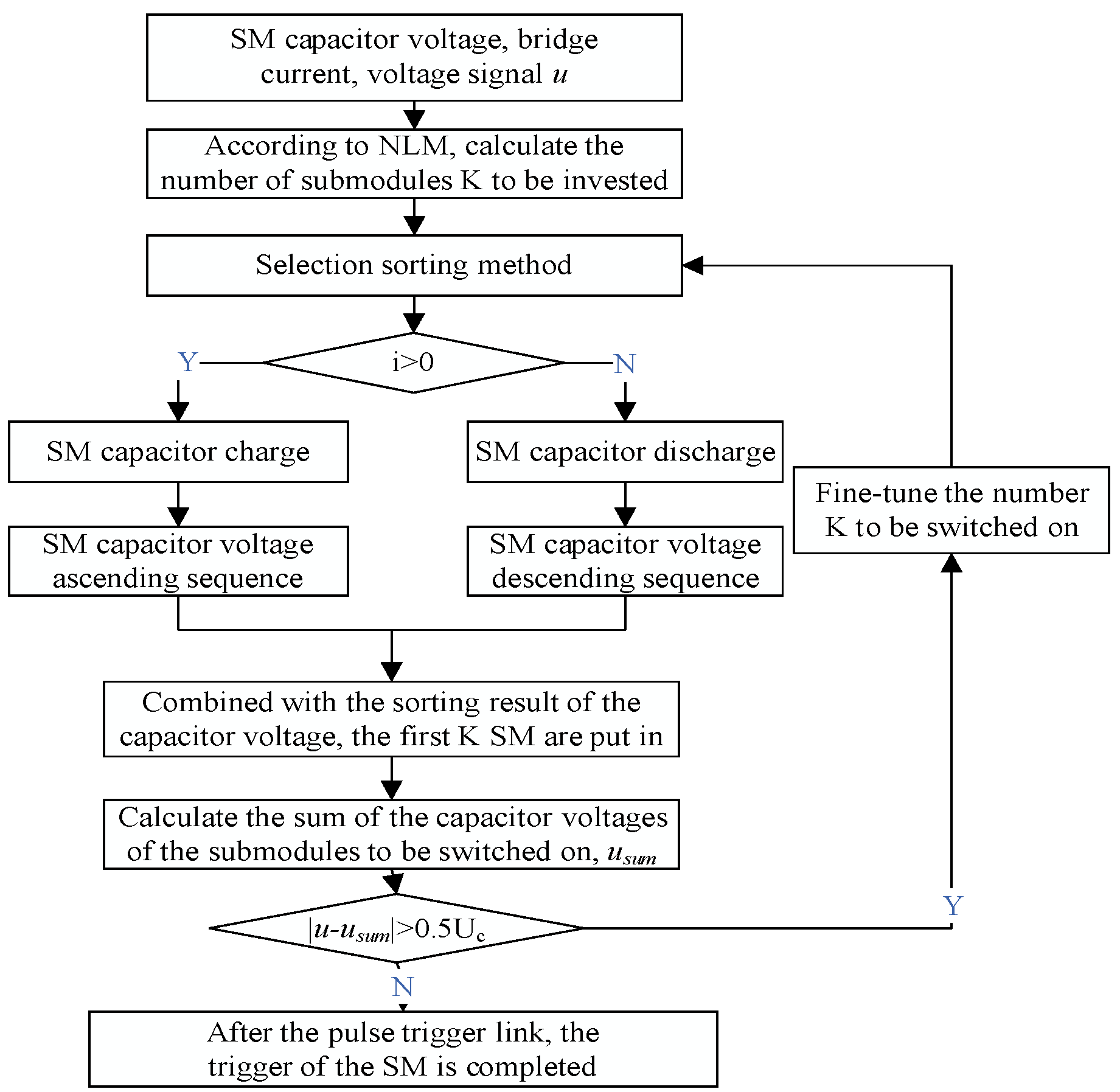
In engineering applications, the NLM modulation strategy requires the collaboration of SM capacitor voltage sequencing to decline the bridge SM capacitor voltage imbalance. The specific control process is shown in Figure 8.
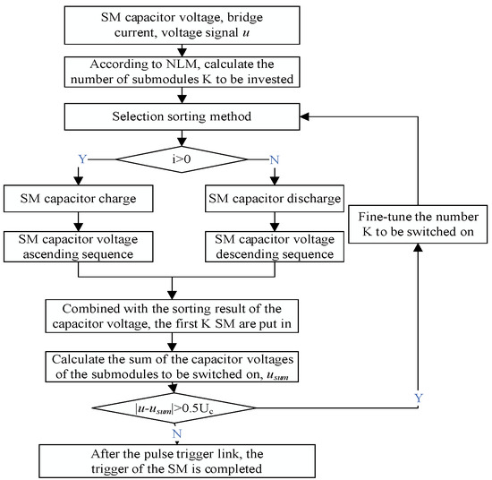
Figure 8.
Traditional capacitor voltage balancing control.
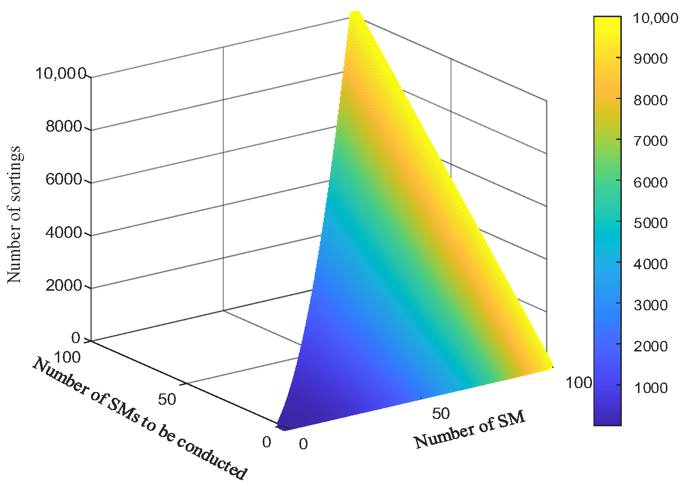
The number of arm SMs, to-be-conducted SMs, and sequencing times are all interconnected, as demonstrated in Figure 9.
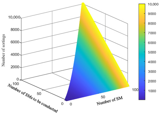
Figure 9.
Relationship between the number of bridge SMs, to-be-conducted SMs, and ordering counts.
4. Presentation Methodology
Upon investigation, it was discovered that each bridge in the ±500 kV Yanqing converter station of the Zhangbei Flexible HVDC Transmission Project contains 264 SMs [28,29]. During operation, relying on multiple sensors to gather the output voltage and bridge current from each SM in real time is essential. Furthermore, the complexity of voltage balancing control is evidently increased by employing the traditional sorting algorithm, highlighting the higher requirements for the controller’s performance. If we suppose that the predictive method is used to derive every SM capacitor voltage and bridge current, then, by doing so, the sensor’s measurement delay and number can be shortened, and the system’s cost can be decreased. The deviation between the actual and theoretical values of capacitor voltage is estimated, a mixed Gaussian distribution with voltage deviation is constructed, and the predicted voltage is compensated to reduce the capacitor voltage deviation. The neural network is utilized to predict the SM triggering sequence and complete the activation to enhance the SM capacitor voltage balancing control speed.
4.1. Time Series Prediction
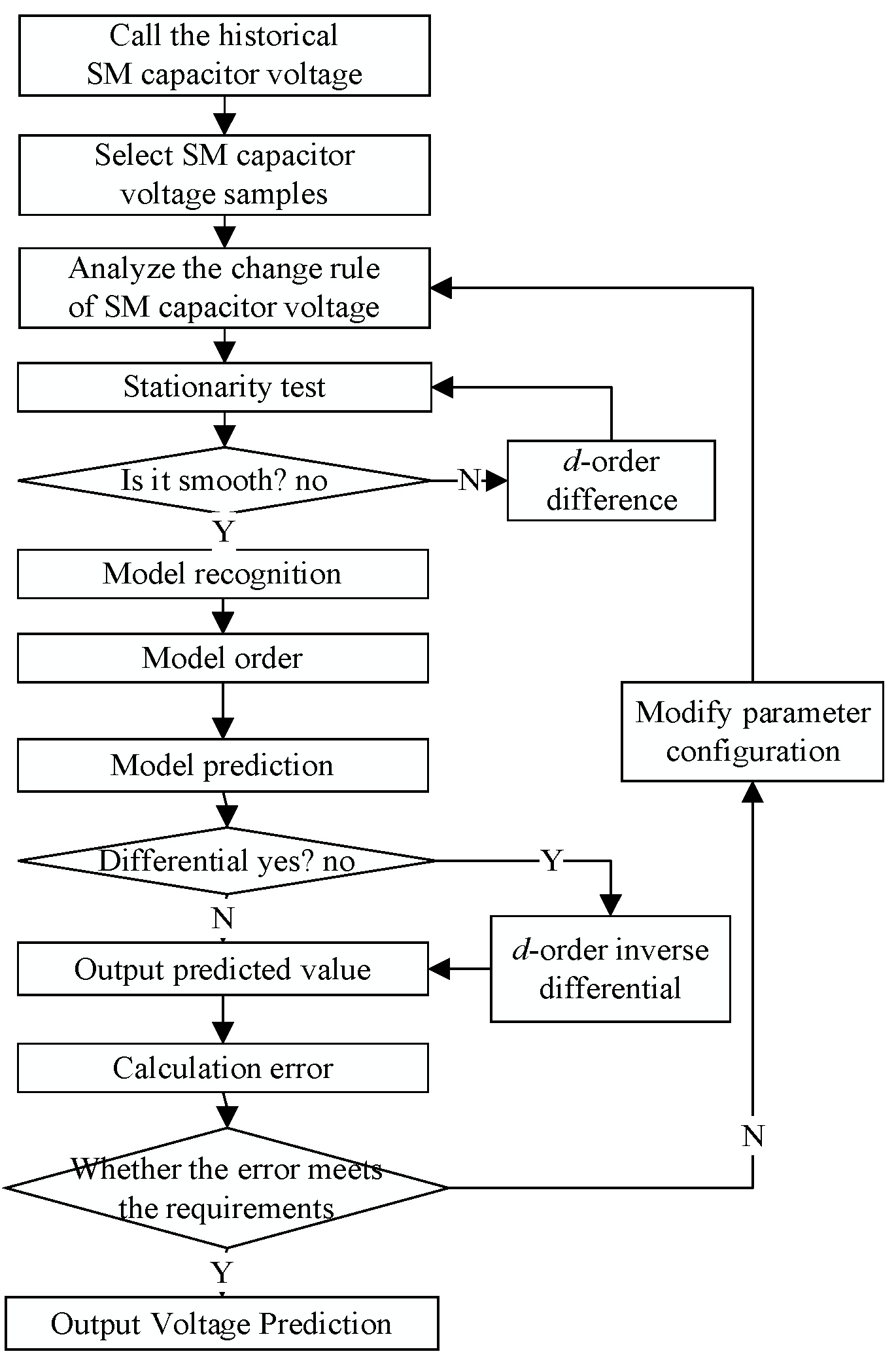
The time series method is introduced to predict the SM capacitor voltage and arm current. The forecasting model changes with MMC’s operating status variation. When the MMC operates steadily, the SM capacitor voltage and arm current are periodic, and the auto-regressive (AR) model is invoked. Conversely, the auto-regressive integrated moving average (ARIMA) model is required. The estimation procedure for the SM capacitor voltage is shown in Figure 10.
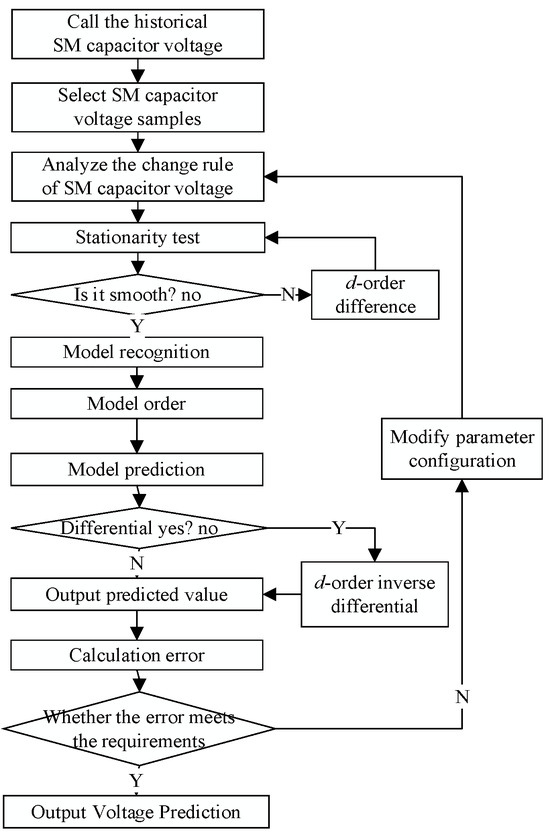
Figure 10.
Prediction process for SM capacitor voltage.
As shown in Figure 10, when the time series prediction method is exploited, it is crucial to ensure that the SM capacitor voltage and arm current are stable. The time series uc(t) is generated from the SM capacitor voltage’s historical record value, and the smoothness test is performed. If the steadiness is not satisfied, then a new sequence uc1(t) is formed to meet the stability requirement by implementing d-order differences. Assuming the period T = 0.02 (s), the time series uc1(t) is examined to ascertain whether it conforms to the following equation:
If the time series uc1(t) satisfies Equation (22), the MMC is operating steadily. The AR model is invited to determine its order by combining the Akaike information criterion (AIC) and the Bayes information criterion (BIC). The specific AIC and BIC criteria are as follows:
Here, k is the number of parameters or the order of the model; n is the number of samples; and L is the likelihood function of the sample composition.
If we suppose the sampling time T1 = 0.000002 (s), then the SM capacitor voltage predicted value uc1(t + T1) is
In Equation (23), ki satisfies the following relationship:
If the time series uc1(t) does not satisfy Equation (22), then an ARIMA model is established, which means that MMC is working in an unstable state. Then, the order p and q are determined, respectively, by the autocorrelation function (ACF) and partial autocorrelation function (PACF). According to the auto-regressive moving average (ARMA) model, the prediction of the stationary sequence uc1(t + T1) is completed:
Here, is an autoregressive coefficient; is a moving average coefficient; and is a random disturbance in this term.
Finally, the SM capacitor voltage uc(t + T1) is found via the d-order inverse difference of the stationary sequence uc1(t + T1). The arm current i(t + T1) can be obtained utilizing the aforementioned method. We define the prediction error h as
Here, pr and tr represent the predicted and actual values, respectively.
According to Equation (30), the SM capacitor voltage and arm current prediction inaccuracy are revealed.
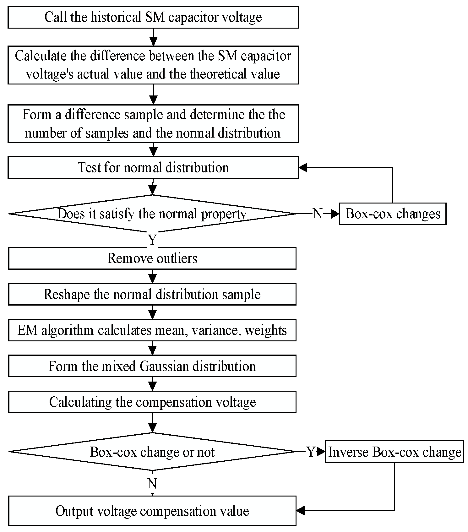
4.2. Constructing Mixed Gaussian Distributions
In actual operation, the SM capacitor parameters are not the same, making the SM charging and discharging rates differ, resulting in a deviation between the virtual and theoretical values for the capacitor voltage and causing an imbalance in the SM stored energy. Therefore, assessing the capacitor voltage error is necessary to establish a mixed Gaussian deviation distribution and estimate the deviation compensation value. The construction process for the mixed Gaussian distribution is shown in Figure 11.
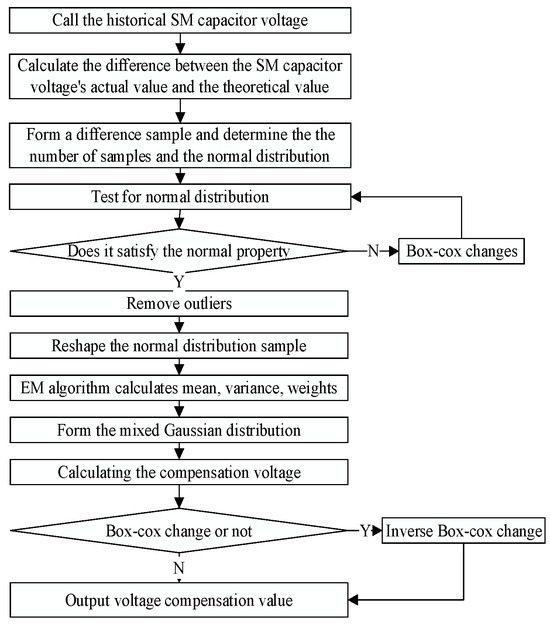
Figure 11.
Construction of the mixed Gaussian distribution for the SM capacitor voltage deviation.
From Figure 11, it can be seen that, firstly, it is vital to perform a standard distribution test (Jarque-Bera test, jbtest) [30] on SM capacitor voltage deviation samples, compute the skewness and kurtosis of this offset, and fabricate the JB statistic:
According to Equations (31)–(33), the corresponding probability (p) is produced and compared with the set significance level (alpha) if p > alpha, indicating that the deviation satisfies the normal distribution. Conversely, it is necessary to use the Box–Cox transformation to contend the normal distribution. The specific transformation rules are as follows:
Here, represents the variation parameter. If the error x < 0, then it is important to add the deviation x to the constant c and continue Equation (34).
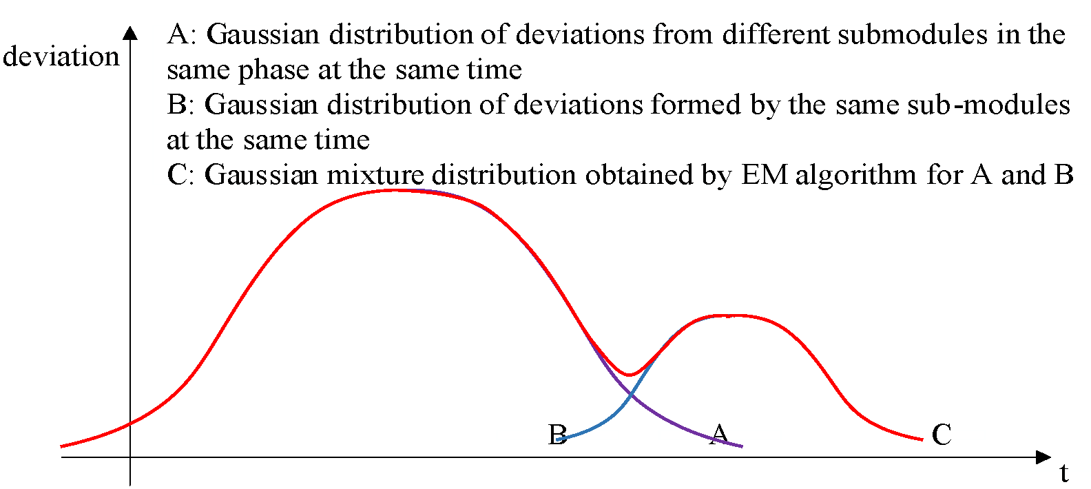
Secondly, the outliers are eliminated based on the significance level (alpha), and the Gaussian samples are reshaped by combining the calculated means so that the number of samples in each Gaussian distribution is the same. Thirdly, each Gaussian distribution’s mean and variance and their corresponding weights are received by using the expectation–maximization algorithm (EM) to form the mixing Gaussian distribution at the i-th moment, as shown in Figure 12. Finally, the compensated value of the SM capacitor voltage deviation is determined by employing the mixed Gaussian distribution.
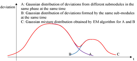
Figure 12.
Mixed Gaussian distribution at i moment.
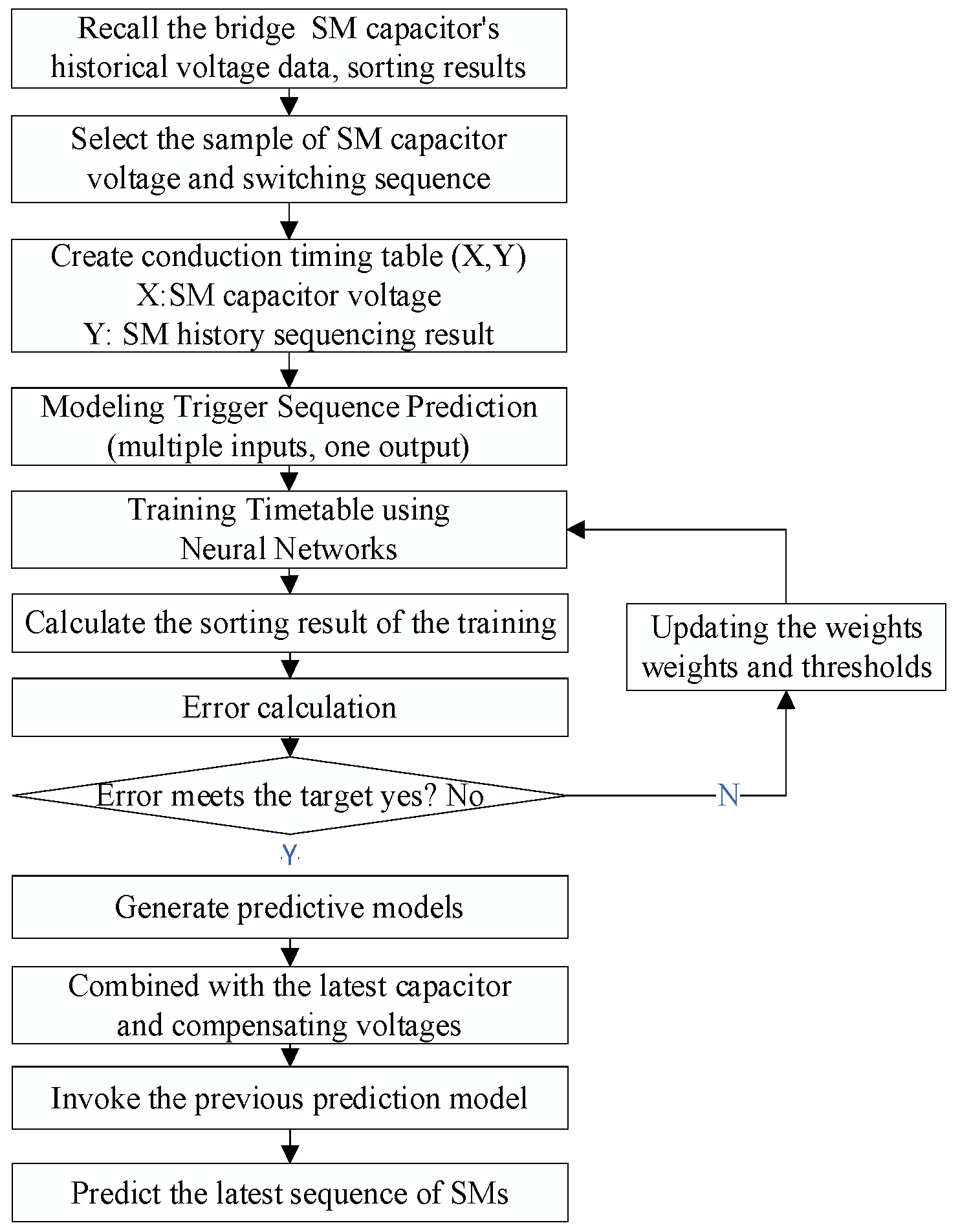
4.3. SM Trigger Sequence Prediction
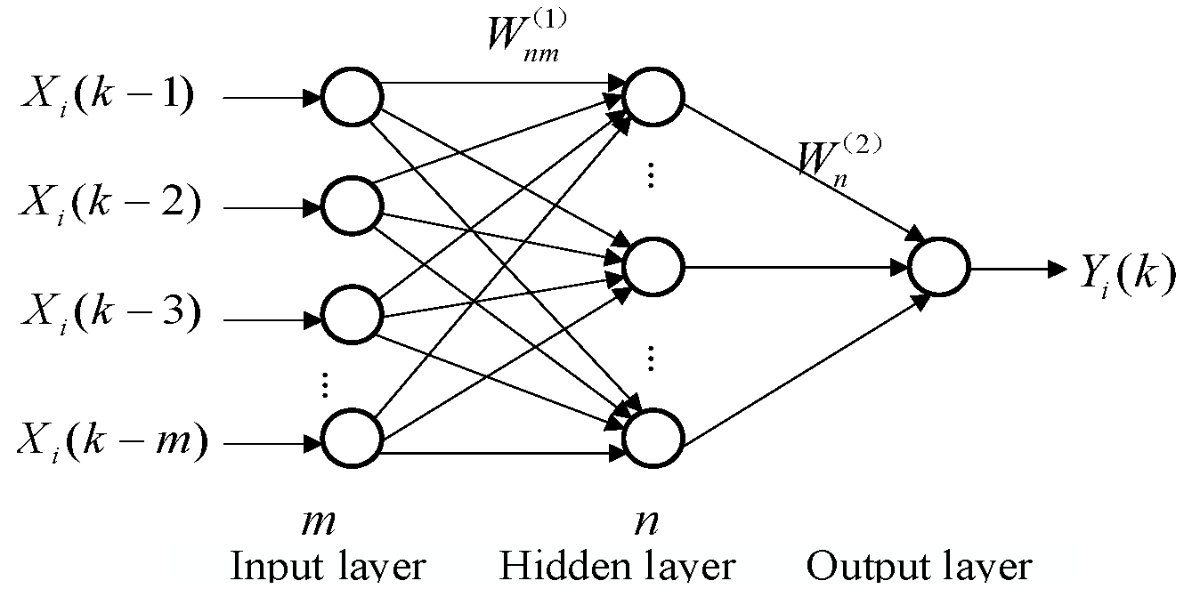
Figure 9 shows that the traditional voltage balance control strategy largely depends on the sorting results for SM capacitor voltage. The time consumption of traditional voltage balancing control increases as the number of SMs grows, resulting in an apparent enlargement in the complexity of the sorting algorithm. When the neural network is applied in the SM capacitor voltage balance control link, it can not only achieve the goal of predicting the SM triggering sequence but also raise the MMC’s response speed. Its model is shown in Figure 13, below.
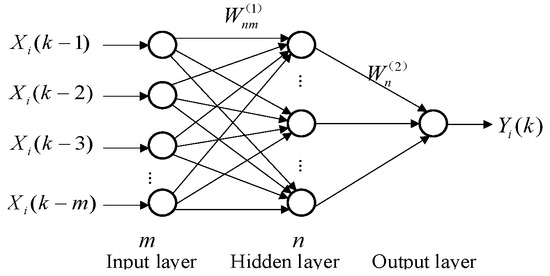
Figure 13.
The model of the neural network.
In Figure 13, Xi(k − a)(a = 1, 2, 3…, m) and Yi(k) denote the a-th input and the k-th output from the i-th sample, respectively. In the neural network, Xi, , , Yi are represented as shown in Table 3, below.
Table 3.
Different letter sizes in neural networks and their meanings.
It is assumed that the actual output and the computed output of forward propagation from the i-th training sample are Qi and Yi, respectively. Then, the error e1 is
The relationship between the calculation error e1 and the setting error e_ref is
If Equation (36) holds, it means that the neural network training meets the requirements. Therefore, the threshold B1 of the neural network hidden layer neurons, the weight W1 from the input layer to the hidden layer, the threshold B2 of the output layer neurons, and the weight W2 from the hidden layer to the output layer are saved. Conversely, backpropagation is performed, and B1, W1, B2, and W2 are updated using the learning factor α. The specific update rules are
Here, W1_t−1, B1_t−1, W2_t−1, and B2_t−1 represent W1, B1, W2, and B2, respectively, at the previous moment. b1 indicates the hidden layer output of the neural network, and its value is
When the neural network is used to estimate the SM trigger sequence, firstly, a timetable named “SM capacitor voltage—conduction sequence” is built based on the SM conduction sequence history; secondly, the neural network is operated to train the timetable, so that the accepted conduction sequence can be close to the actual SM conduction order. Finally, a “multiple-input–single-output” anticipating model is generated and merged with the latest collected SM capacitor voltages to complete the SM conduction sequence prediction; the specific flow is shown in Figure 14.
Figure 14.
Neural network predicts the SM’s conduction sequence.
Figure 14 shows a strong correlation between the selected SM conduction sequence samples and the neural network’s forecasting precision. Depending on whether the training sample N fluctuates, the prediction method is further separated into fixed data sample prediction, fixed timescale prediction, and variable timescale prediction.
5. Simulation Results
Firstly, the MMC model with three phases, six bridges, and eight SMs is built in Matlab/Simulink. Together with the MMC control target, the NLM modulation strategy is used to perform the SM capacitor voltage balancing control by combining the bubbling method.
Secondly, the SM capacitor voltage, arm current, and conductance sequence are recorded in real time under the traditional voltage balancing control strategy.
Thirdly, time series prediction, grey prediction, Gaussian prediction, exponential smoothing, and other approaches are exploited to predict the SM capacitor voltage and arm current. The above methods’ forecasting precision and time delay are measured and compared.
Finally, the mixed Gaussian distribution of the voltage deviation is produced, and its compensation value is computed. The SM trigger sequence is determined and completed by manipulating the neural network. The feasibility of the prediction method is verified via simulation.
Taking the passive inverter as an example, when the MMC is operating in the inactive inverter state, the parameters of the MMC are configured, as shown in Table 4, below.
Table 4.
Parameter configuration of MMC working in the passive inverter state.
5.1. Voltage and Current Prediction
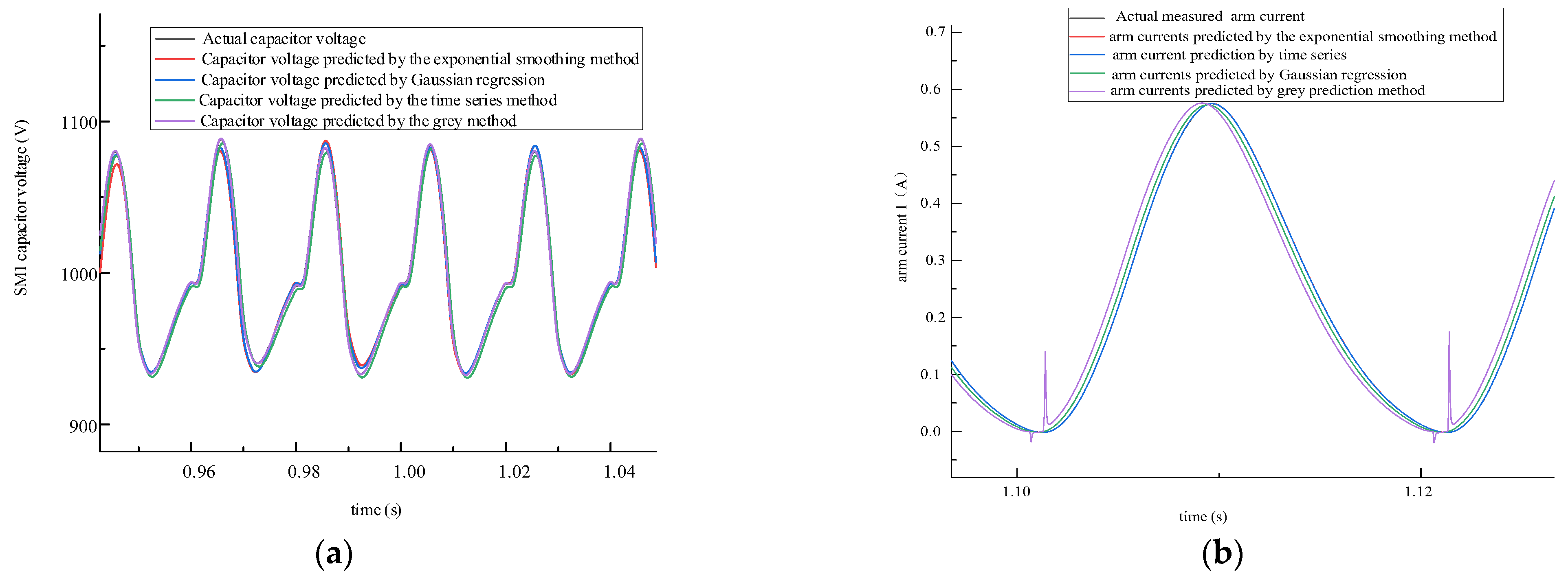
When the MMC operating parameters are not changed, the SM capacitor voltage variation curve, the arm current variation curve, and their prediction curve are as shown in Figure 15.
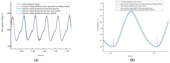
Figure 15.
SM capacitor voltage, arm current variation curve, and their prediction curve. (a) SM capacitor voltage variation curve. (b) Arm current variation curve.
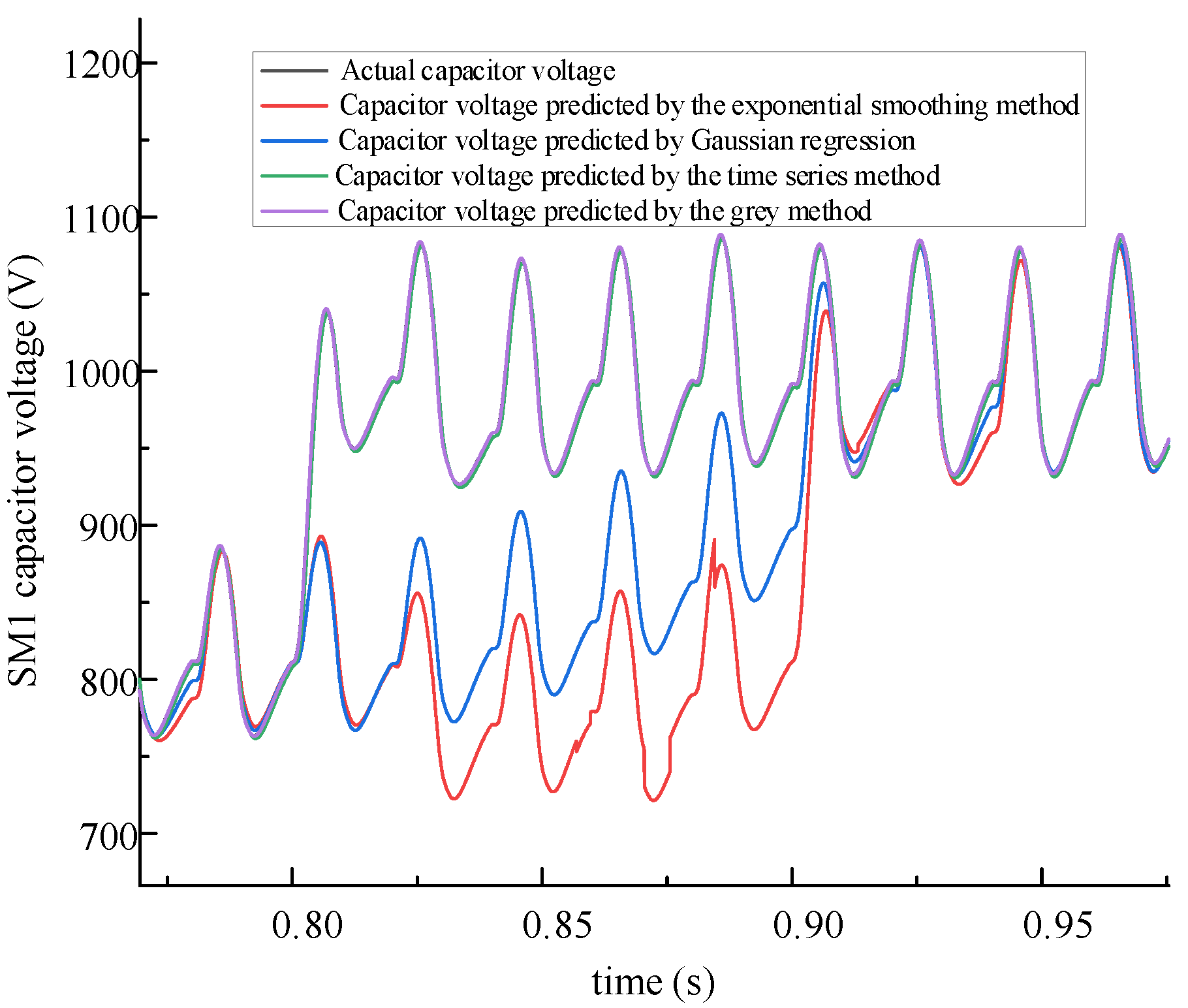
When the MMC operating parameters are changed, the SM capacitor voltage variation curve and its prediction curve are as shown in Figure 16.
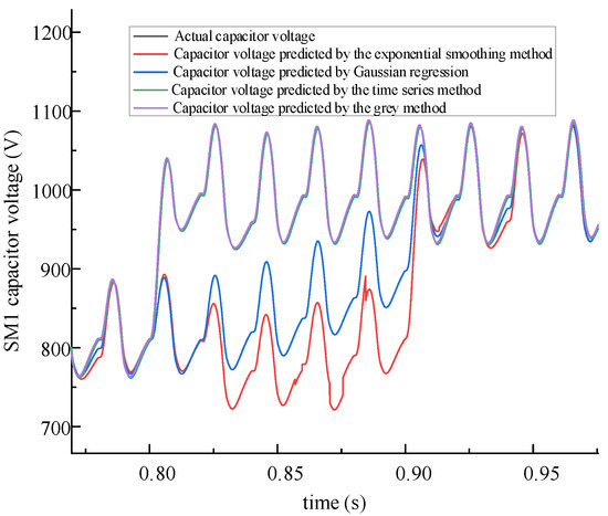
Figure 16.
SM capacitor voltage variation curve and its prediction curve.
Combined with Equation (28), different methods’ prediction delay and accuracy are evaluated, respectively, as shown in Table 5.
Table 5.
Prediction delay and error of different methods.
According to the standard, the devices’ measurement accuracy reaches 0.2 grade [31,32]. The PCB sensor is frequently employed to convey real-time voltage and current in the power system [29]. Two methods are reported in the literature to collect the SM capacitor voltage: the analog-to-digital converter and voltage-controlled oscillator [33]. Comparing Table 5, when the time series prediction tool is utilized, its time delay is much lower than the measurement delay of the PCB sensor. Meanwhile, the time series estimation approach meets practical engineering requirements.
5.2. Constructing Mixed Gaussian Distributions for Voltage Deviations
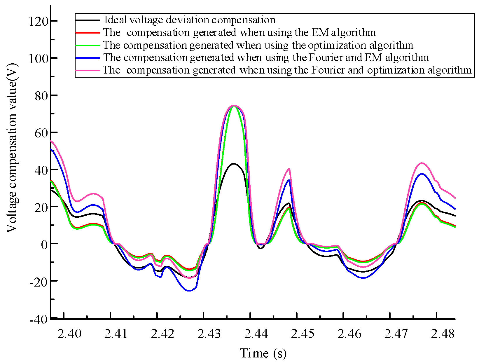
Under the conditions in Table 4, the offset voltage is formed and its compensation value is counted separately, as shown in Figure 17, below.
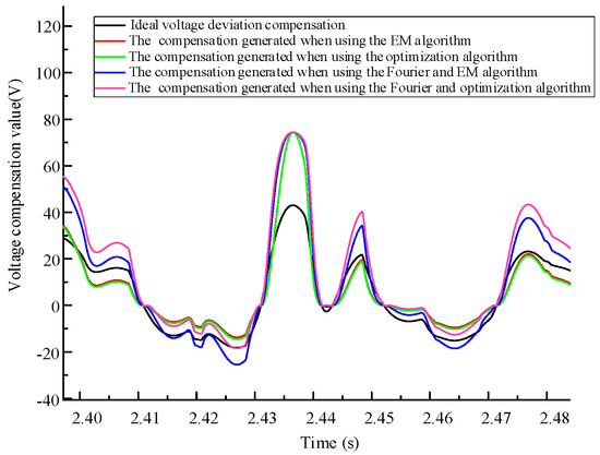
Figure 17.
SM capacitor voltage deviation compensation values with different methods.
As shown in Figure 17, when the mixed Gaussian distribution of voltage offset is fabricated using the EM algorithm and the sampling frequency, its received compensation voltage amount is closest to the ideal voltage deviation compensation amount. Then, the deviation compensation effect is as shown in Figure 18.

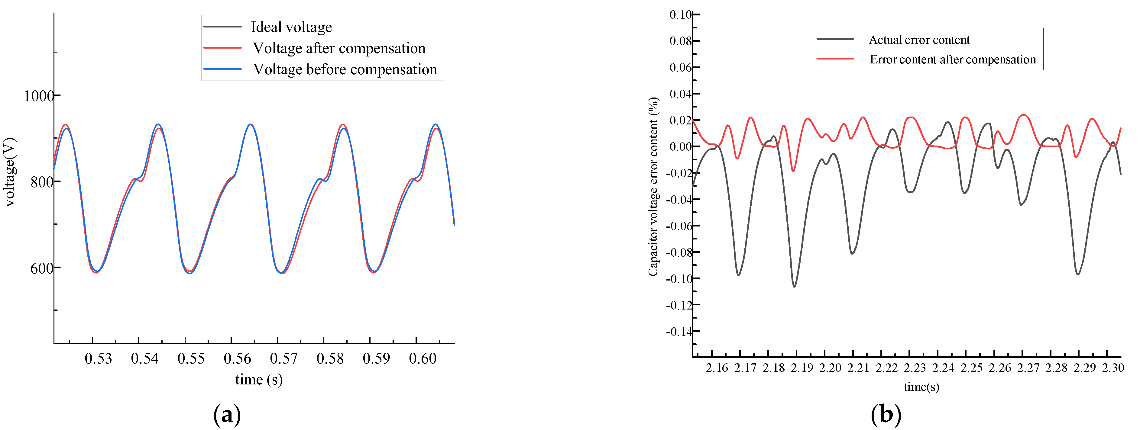
Figure 18.
Before and after compensation, the SM capacitor voltage compensation effect and its error comparison. (a) SM capacitor voltage compensation effect. (b) Error content before and after compensation.
5.3. SM Trigger Sequence Prediction
When the neural network is manipulated to predict the SM trigger sequence, its prediction accuracy and speed are easily influenced by the number of hidden layer neurons and the training samples when the training, validation, and test sets meet different proportions, as shown in Table 6.
Table 6.
Different proportions of the training, validation, and test sets.
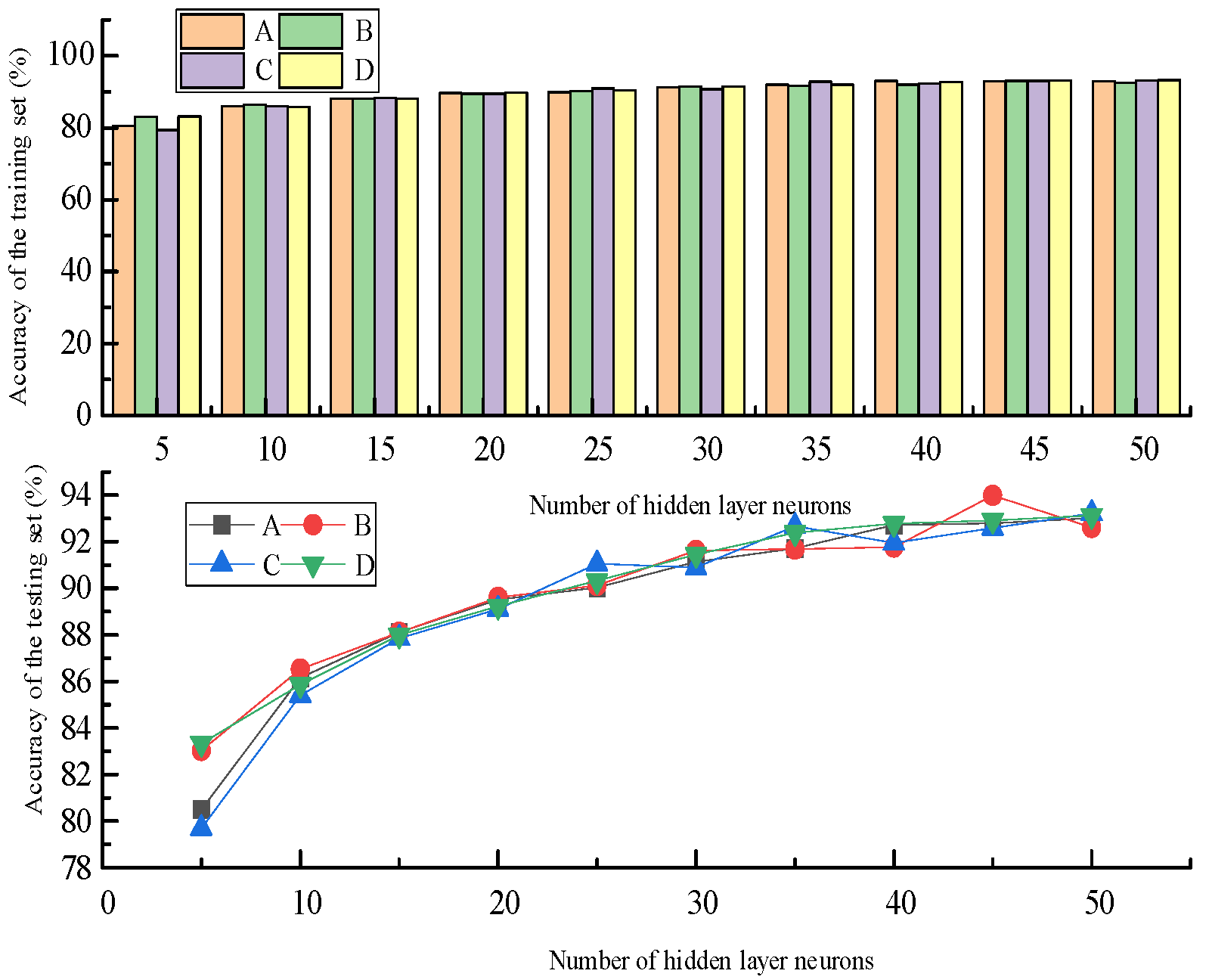
A bar graph represents the training set’s accuracy, and a line graph reflects the test set’s accuracy. At this point, the relationship between the accuracy (%) of its training set and the hidden layer neuron number of the neural network varies, as shown in Figure 19, below.
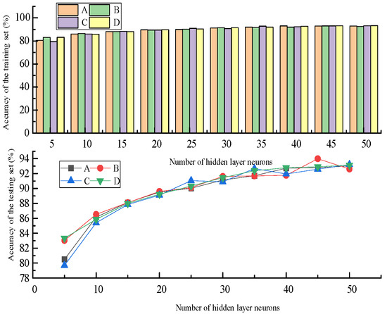
Figure 19.
Relationship between the accuracy (%) of the training set and the number of neurons in the neural network’s hidden layer on different scales.
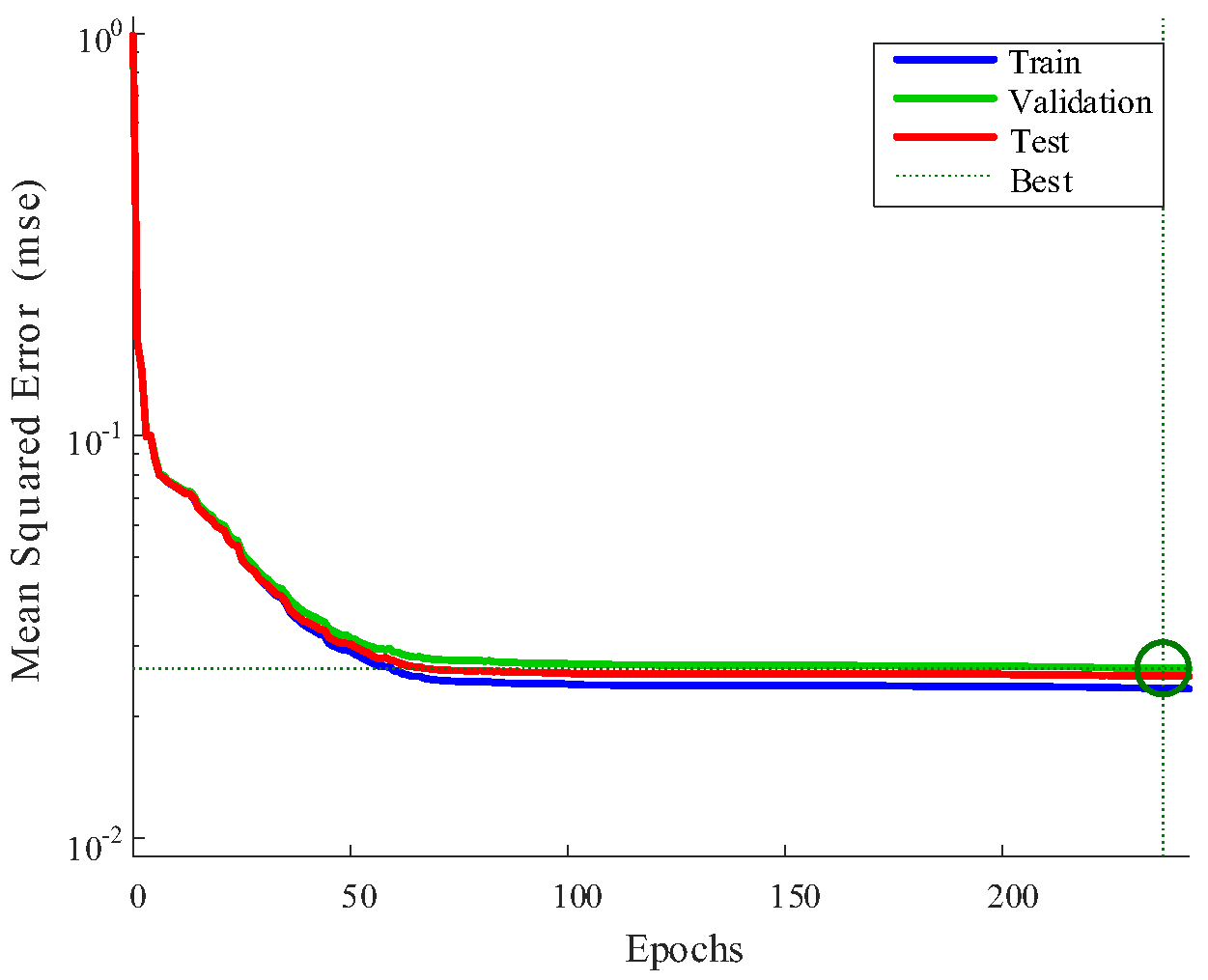
Figure 19 indicates that the neural network forecast accuracy will fluctuate drastically when the training, validation, and test sets encounter different proportions. In particular, when the training, validation, and test sets are 90%, 5%, and 5%, respectively, there is an excellent linear relationship between the neural network prediction accuracy and the number of neurons in the hidden layer. When the number of hidden layer neurons is greater than 40, the accuracy of the training, validation, and test sets gradually slows down. Meanwhile, its mean-square-error variation is shown in Figure 20, below.

Figure 20.
Variation in the mean square error.
It can be seen from Figure 20 that with an increasing number of iterations, the mean square error of the training set gradually decreases. At 237 iterations, the mean square error is the smallest. Therefore, in this prediction mode, the number of hidden layer neurons and iterations is 40 and 300, respectively.
When the neural network is employed to predict the SM conduction sequence, the parameter configuration of the neural network is as shown in Table 7, below.
Table 7.
Parameter configuration of the neural network.
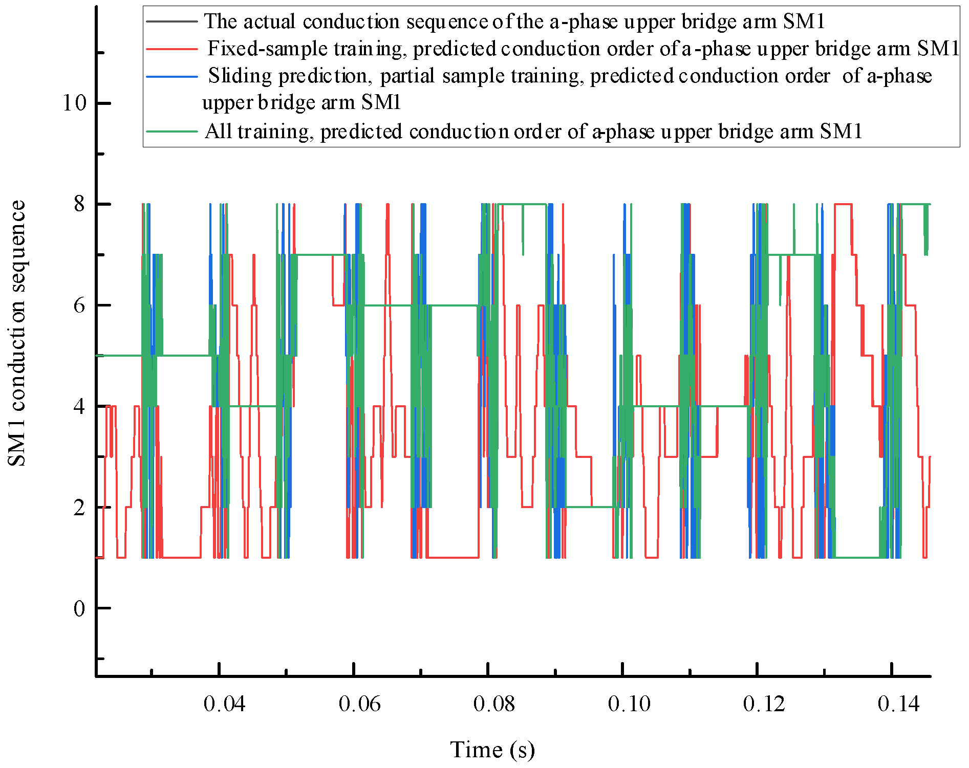
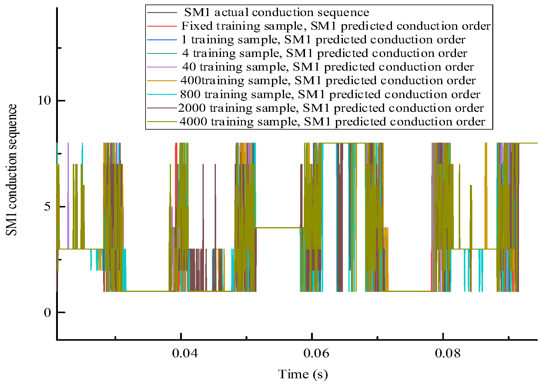
In addition, the prediction method also exerts an essential impact on the forecast accuracy and speed of the neural network. When the neural network uses the fitting approach for estimation, the SM trigger sequence is shown in Figure 21, below.
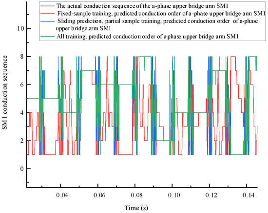
Figure 21.
Neural network predicting the conduction order of SM via fitting under different sample training options.
When the neural network uses the classification approach for prediction, the SM trigger sequence is shown in Figure 22, below.
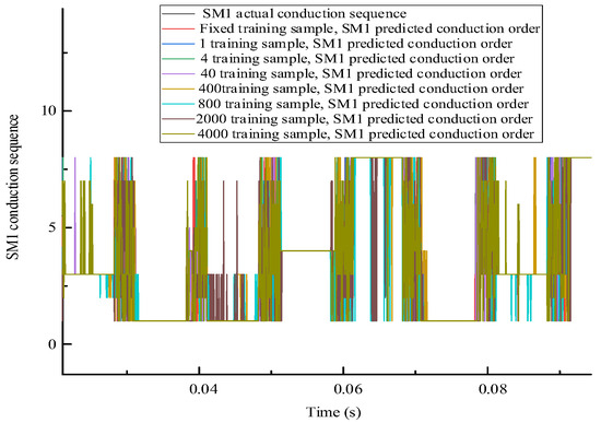
Figure 22.
Neural network predicting the conduction order of SM via classification under different sample training options.
Combining Figure 21 and Figure 22, the neural network forecast accuracy is assessed for various training samples using different methods to predict the SM conduction order, as shown in Table 8.
Table 8.
Prediction accuracy and speed of SM trigger sequence.
As seen in Table 8, the neural network estimation speed is closely related to the training samples. The smaller the scale of the samples, the fewer iterations in the training session, and the faster predictions are made. Fixed initialization under the same sample scale significantly improves the neural network forecast speed.
In practical engineering, firstly, the fixed data samples are selected to train the neural network; secondly, the trained neural network is fine-tuned with the variable data samples to generate a suitable model; and, finally, the prediction of the SM conduction sequence is accomplished by merging the latest SM capacitor voltage. At this time, the output voltage uj of the harmonic content is as shown in Table 9, below.
Table 9.
Harmonic content of uj before and after prediction.
From Table 9, it can be seen that the neural network prediction method satisfies the accuracy of control requirements. If we imagine that the number of SMs in each bridge and hidden layer in the neural network are m and n, separately, then, as a result, the time complexity of the neural network and the sorting algorithm are O(2mn + m + n) and O(m2), respectively. When is satisfied, the forecast time delay of the neural network will be less than that of the bubble sort.
6. Conclusions
The reasons for SM capacitor voltage imbalance are examined in this paper from two perspectives: the SM capacitor values and the modulation mechanism. The adverse impacts of SM capacitor voltage imbalance are explored in detail, such as boosting the circulating current, relaxing the usage of the DC voltage, and giving rise to overheating and vibration in specific SMs.
The time series prediction technique is implemented based on historical values to forecast the SM capacitor voltage and arm current in real time. The mixed Gaussian distribution of the capacitor voltage offset is developed, and the compensation voltage is calculated. The usual sorting method is used to produce the trigger sequences, regarded as a sample to train the neural network. Then, the prediction of the SM trigger sequence and the completion of the control are achieved by uniting the anticipated values for the SM capacitor voltage, the arm current, and the compensation value for voltage deviation.
The SM capacitor voltage balancing control strategy based on neural network prediction is verified via Matlab/Simulink simulation. It improves the speed while satisfying the accuracy and provides an idea for the subsequent intelligent control of the capacitor voltage balance.
Author Contributions
Writing—original draft, Q.X.; Writing—review & editing, Y.T.; Funding acquisition, Y.F. All authors have read and agreed to the published version of the manuscript.
Funding
This work was supported in part by the National Key Research and Development Program of China (2021YFB1507000).
Data Availability Statement
Data will be made available on request.
Conflicts of Interest
The authors declare that they have no known competing financial interests or personal relationships that could have appeared to influence the work reported in this paper.
References
- Debnath, S.; Qin, J.; Bahrani, B.; Saeedifard, M.; Barbosa, P. Operation, Control, and Applications of the Modular Multilevel Converter: A Review. IEEE Trans. Power Electron. 2015, 30, 37–53. [Google Scholar] [CrossRef]
- Ferreira, J.A. The Multilevel Modular DC Converter. IEEE Trans. Power Electron. 2013, 28, 4460–4465. [Google Scholar] [CrossRef]
- Ludois, D.C.; Venkataramanan, G. Simplified Terminal Behavioral Model for a Modular Multilevel Converter. IEEE Trans. Power Electron. 2013, 29, 1622–1631. [Google Scholar] [CrossRef]
- Li, Y.; Jones, E.A.; Wang, F. The impact of voltage-balancing control on switching frequency of the modular multilevel converter. IEEE Trans. Power Electron. 2015, 31, 2829–2839. [Google Scholar] [CrossRef]
- Qiang, S.; Wenhua, L.; Xiaoqian, L.; Jianguo, L.I.; Yu, L.U.O. Analytical Method for Analysis on Steady-State Operating Characteristics of Modular Multilevel Converter. Power Syst. Technol. 2012, 36, 198–204. [Google Scholar]
- Kolluri, S.; Gorla, N.B.Y.; Panda, S.K. Capacitor Voltage Ripple Suppression in a Modular Multilevel Converter Using Frequency-Adaptive Spatial Repetitive-Based Circulating Current Controller. IEEE Trans. Power Electron. 2020, 35, 9839–9849. [Google Scholar] [CrossRef]
- Shang, M.; Yi, W. Research on Strategy for Capacitor Voltage Balancing of Modular Multilevel Converter. Mod. Electr. Power 2015, 32, 50–55. [Google Scholar]
- Chen, J.; Zhang, C.; Wang, Z.; Li, G.; Xin, Y.; Dong, F. Strategy Research and Simulation Analysis of Current Ripple Suppression for MMC-HVDC Converter Station. Power Syst. Technol. 2018, 42, 3842–3849. [Google Scholar]
- Lu, M.; Hu, J.; Zeng, R.; Li, W.; Lin, L. Imbalance Mechanism and Balanced Control of Capacitor Voltage for a Hybrid Modular Multilevel Converter. IEEE Trans. Power Electron. 2017, 33, 5686–5696. [Google Scholar] [CrossRef]
- Wang, W.; Ma, K.; Cai, X. Flexible Nearest Level Modulation for Modular Multilevel Converter. IEEE Trans. Power Electron. 2021, 36, 13686–13696. [Google Scholar] [CrossRef]
- Li, Z.; Gao, F.; Xu, F.; Ma, X.; Chu, Z.; Wang, P.; Gou, R.; Li, Y. Power Module Capacitor Voltage Balancing Method for a ±350-kV/1000-MW Modular Multilevel Converter. IEEE Trans. Power Electron. 2015, 31, 3977–3984. [Google Scholar] [CrossRef]
- Joshi, S.D.; Ghat, M.B.; Shukla, A.; Chandorkar, M.C. Improved Balancing and Sensing of Submodule Capacitor Voltages in Modular Multilevel Converter. IEEE Trans. Ind. Appl. 2020, 57, 537–548. [Google Scholar] [CrossRef]
- Peng, H.; Xie, R.; Wang, K.; Deng, Y.; He, X.; Zhao, R. A Capacitor Voltage Balancing Method with Fundamental Sorting Frequency for Modular Multilevel Converters Under Staircase Modulation. IEEE Trans. Power Electron. 2016, 31, 7809–7822. [Google Scholar] [CrossRef]
- Zhang, J.; Zeng, G.; Zhao, J.; Huang, B.; Xiao, B. Modular multilevel converter capacitor voltage balancing strategy based on improved bubble sorting. Power Syst. Prot. Control 2020, 48, 92–99. [Google Scholar]
- Rong, F.; Xu, Y.; Huang, S.; Li, X. Optimized Voltage Balancing Strategy Based on Radix Sort Algorithm for Modular Multilevel Converter. Proc. CSU-EPSA 2018, 30, 42–49. [Google Scholar]
- Gou, X.; Lu, J.; Liu, J.; Xu, Y.; He, Q. A Capacitor Voltage Balancing Control Method for Modular Multilevel Converter Based on Insertion Priority of the Sub-modules. Proc. CSEE 2019, 39, 7299–7310+7503. [Google Scholar]
- Gou, R.; Zhao, F.; Xiao, G.; Tu, X. A Capacitor Voltage Balancing Strategy for MMC Based on Optimized Merge Sort. Proc. CSEE 2017, 37, 251–261. [Google Scholar]
- Abushafa, O.S.H.M.; Dahidah, M.S.A.; Gadoue, S.M.; Atkinson, D.J. Submodule Voltage Estimation Scheme in Modular Multilevel Converters with Reduced Voltage Sensors Based on Kalman Filter Approach. IEEE Trans. Ind. Electron. 2018, 65, 7025–7035. [Google Scholar] [CrossRef]
- Viatkin, A.; Ricco, M.; Mandrioli, R.; Kerekes, T.; Teodorescu, R.; Grandi, G. Sensorless Current Balancing Control for Interleaved Half-Bridge Submodules in Modular Multilevel Converters. IEEE Trans. Ind. Electron. 2022, 70, 5–16. [Google Scholar] [CrossRef]
- Baagheri-Hashkavayi, M.; Barakati, S.M.; Yousofi-Darmian, S.; Barahouei, V. Improved Sensor Reduction Method in Modular Multilevel Converters with Open-Loop Controller Based on Arms Energy Estimation. IEEE Trans. Power Deliv. 2022, 37, 5003–5013. [Google Scholar] [CrossRef]
- Liu, H.; Zhao, C.; Zhou, J.; Hi, L.; Li, S.; Xu, J. Novel Topology of Modular Multilevel Converter with Voltage Self-balancing Ability. Proc. CSEE 2017, 37, 5707–5716+5848. [Google Scholar]
- Yin, T.; Wang, Y.; Wang, X.; Yin, S.; Sun, S.; Li, G. Modular Multilevel Converter with Capacitor Voltage Self-Balancing Using Reduced Number of Voltage Sensors. In Proceedings of the 2018 International Power Electronics Conference (IPEC-Niigata 2018-ECCE Asia), Niigata, Japan, 20–24 May 2018; pp. 1455–1459. [Google Scholar]
- Zhang, J.; Cui, D.; Tian, X.; Zhao, C. Self-Block and Voltage Balance Modular Multilevel Converter Sub Module Topology and Control. Trans. China Electrotech. Soc. 2020, 35, 3917–3926. [Google Scholar]
- Le, D.D.; Lee, D.C.; Nho, E.C. Capacitor Voltage-Balancing Control for Flying-Capacitor MMC without Current Sensors. In Proceedings of the 2020 IEEE 9th International Power Electronics and Motion Control Conference (IPEMC2020-ECCE Asia), Nanjing, China, 29 November–2 December 2020; pp. 1765–1770. [Google Scholar]
- Hu, Y.; Liu, Y.; Zhang, S.; Lin, W. Dynamic Range Segmented Sorting Algorithm Based Voltage Balance Method for MMC Submodule. South. Power Syst. Technol. 2018, 12, 27–33+40. [Google Scholar]
- Wang, Y.; Liu, C.; Li, G.; Sun, J.; Wu, S. Capacitor Voltage Balancing Control Method for Modular Multilevel Converter Applicable for FPGA. Autom. Electr. Power Syst. 2019, 43, 167–173. [Google Scholar]
- Hu, P.; Teodorescu, R.; Wang, S.; Li, S.; Guerrero, J.M. A Currentless Sorting and Selection-Based Capacitor-Voltage-Balancing Method for Modular Multilevel Converters. IEEE Trans. Power Electron. 2018, 34, 1022–1025. [Google Scholar] [CrossRef]
- Tang, G. 500 kV Research on Key Technology and Equipment for 500 kV DC Grid. High Volt. Eng. Electrotech. Appl. 2018, 37, 4–7. [Google Scholar]
- Tang, G.; Wang, G.; He, Z.; Pang, H.; Zhou, X.; Shan, Y.L. Research on Key Technology and Equipment for Zhangbei 500 kV DC Grid. High Volt. Eng. 2018, 44, 2097–2106. [Google Scholar]
- GB/T 24841-2018; National Technical Committee for Standardization of UHV AC Transmission (SAC/TC 569). State Administration for Market Regulation, Standardization Administration of the People’s Republic of China: Beijing, China, 2018.
- GB/T 20840.5-2013; National Technical Committee for Standardization of Instrument Transformer (SAC/TC 222). General Administration of Quality Supervision, Inspection and Quarantine of the People’s Republic of China, Standardization Administration of the People’s Republic of China: Beijing, China, 2013.
- Glinka, M. Prototype of multiphase modular-multilevel-converter with 2 MW power rating and 17-level-output-voltage. In Proceedings of the 2004 IEEE 35th Annual Power Electronics Specialists Conference (IEEE Cat. No. 04CH37551), Aachen, Germany, 20–25 June 2004; Volume 4, pp. 2572–2576. [Google Scholar] [CrossRef]
- Shuoran, J.I.A.N.G.; Yarui, C.H.E.N.; Zhifei, Q.I.N.; Jucheng, Y.A.N.G. Split and merge algorithm for Gaussian mixture model based on KS test. J. Univ. Sci. Technol. China 2018, 48, 477–485. [Google Scholar]

Disclaimer/Publisher’s Note: The statements, opinions and data contained in all publications are solely those of the individual author(s) and contributor(s) and not of MDPI and/or the editor(s). MDPI and/or the editor(s) disclaim responsibility for any injury to people or property resulting from any ideas, methods, instructions or products referred to in the content. |
© 2024 by the authors. Licensee MDPI, Basel, Switzerland. This article is an open access article distributed under the terms and conditions of the Creative Commons Attribution (CC BY) license (https://creativecommons.org/licenses/by/4.0/).