Abstract
ZnO nanowire is a promising candidate for large-area gated field emitter arrays. How to improve its temporal response is one of the key problems to be solved for applications. In this work, a device model for a gated ZnO nanowire field emitter with consideration of charging and self-heating effect has been established to investigate its temporal response. It is found that while the charging effect is responsible for the delay at the beginning of the pulse, the self-heating effect which induces delay due to the thermal conduction process can shorten the charging time because of its lowering of nanowire resistance. The response time can be minimized when these two effects are balanced at an optimal field which is below the critical field for thermal runaway. We further investigate the optimal response time of a nanowire with the same resistance but a different length, radius, and electrical properties. The results imply that a lower heat capacity and higher critical temperature for thermal runaway are in favor of a shorter response time, which must be taken into account in the reduction in nanowire resistance for improving response speed. All the above should be useful for the device design of a fast-response gated ZnO nanowire field emitter array.
1. Introduction
Field emitter array has important applications in field emission display [1,2,3,4,5], parallel electron-beam lithography [6,7,8,9], and X-ray source [10,11,12,13,14,15]. Until now, only CNT [16], Si nanotip [17], and ZnO nanowire [18] have been active in studies of field emitter array applications. Among them, ZnO nanowire has advantages in terms of its simple synthesis method, low cost, high uniformity, and compatibility with microfabrication techniques, which makes it outstanding in large-area gated field emitter arrays [18]. One of the key problems in its commercialization is how to further improve response speed, which is important for realizing the addressing or fast imaging function in a flat-panel X-ray source with desirable frequency.
So far, the temporal responses of several kinds of quasi-one-dimensional field emitters have been reported. It is found that the response time of CNT can be down to ~100 ns [19,20], while that for individual SiC nanowire is ~1 ms [21]. For ZnO nanowire, the response time is tens of microseconds in a MOSFET controlled device [22]. Here, it should be noted that the plasma-induced electron emission [23,24,25] is not considered since it requires a pulsed voltage of more than 104 V, which is difficult to apply in a gated structure. This large difference in response time from different materials is related to the charging process under the pulsed driving voltage. Basically, in a gated field emitter device, as shown in Figure 1a, there are two charging processes. One is due to the capacitance C0 between gate and cathode electrodes that induces a delay for the actual voltage on the gate Ug. The other is due to the capacitance C between gate and emitter that induces a delay for the actual voltage difference Uc. The equivalent circuit can be seen schematically in Figure 1b, where R and R0 are the resistance of the emitter and electrode, respectively. Compared to CNT, SiC and ZnO nanowire have higher resistance due to their wide-bandgap semiconductor properties (for SiC nanowire, its piezoresistive effect further increases its resistance [21]), resulting in a longer delay for Uc as well as the field emission current IFE (note that the time for turning on and off IFE, as denoted by t1 and t3 in Figure 1c, is the response time). Therefore, to improve the response speed of a gated ZnO nanowire field emitter, one needs to reduce its nanowire resistance, which can be realized by tunning the resistivity or geometrical structure of the nanowire.
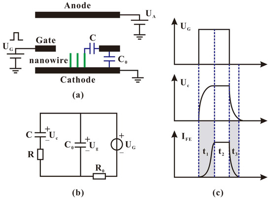
Figure 1.
Schematic diagram of the pulsed response of gated field emitter array. (a) Device structure. (b) Equivalent circuit. UA and UG are the applied voltage on anode and gate. Ug is the actual voltage on the gate. Uc is the actual voltage between gate and emitter. C0 is the capacitance between gate and cathode electrodes. C is the capacitance between gate and emitter. R and R0 are the resistance of emitter and electrode. (c) Pulsed response of UG, Uc, and emission current IFE. t1 and t3 denote the time for turning on and off IFE. t2 denotes the time for device operation.
On the other hand, the self-heating effect which usually exists in the field emission of ZnO nanowire [26,27] could help to further improve the response speed since the semiconductor nanowire’s resistance will be reduced under a high temperature. However, as the temperature increases, a longer delay to obtain a steady thermal field emission current will be induced, which may reduce the response speed. To obtain the optimal response time, the influence of the self-heating effect on the temporal response of the gated ZnO nanowire field emitter needs to be investigated. Moreover, considering that the self-heating process is mainly determined by the electrical properties and geometrical structure of the nanowire, knowledge of the impact of the self-heating effect is also important to guide the tunning of nanowire resistance. All of these require not only experimental but also theoretical studies on the temporal response of pulsed field emission from ZnO nanowire. In theoretical works, although the charging process and self-heating effect have been considered separately in modeling the temporal response of the nanowire field emitter, a device model that takes into account both of them is still lacking, which is necessary for the design of a fast-response gated field emitter array device.
In this work, such a model has been established to investigate the temporal response of a gated ZnO nanowire field emitter. Simulations have been performed under single and continuous pulses, showing the dependence of response time on the pulsed field, that decreases first and then increases. Calculations of the optimal response time of nanowire with the same resistance but different electrical properties or geometrical structure have also been carried out to understand the proper way to tune nanowire resistance.
2. Theoretical Model
Figure 1a illustrates the device structure, where UA is the applied anode voltage, UG is the applied gate voltage (the voltage source is treated as ideal with no delay), and the cathode is grounded. Considering that UA is a constant which has no influence on the response speed of the device, the equivalent circuit for calculating the charging time can be presented as Figure 1b. According to Kirchhoff law,
where t denotes time.
To calculate IFE, the formula of the thermal field emission current density jTFE of thermal oxidized synthesized ZnO nanowire can be adopted, which can be expressed as [26]
where e denotes the electron charge, m is the electron effective mass, k is the Boltzmann constant, h is the Planck constant, v(y) is an elliptic function, , A is the ratio factor balancing the conductance between the nanowire body and surface, Te is the effective electron temperature, EFs is the surface Fermi level, F is the surface electrical field, W is the electron energy normal to the surface, , ε0 is the vacuum dielectric constant, and εr is the relative dielectric constant of ZnO. Here, F = Fa + Fg, where Fa is the anode field and Fg = βUc is the actual gate field (β is the voltage-to-field conversion factor). With consideration of both the tip and sidewall emission from the nanowire when it is self-heating, IFE can be calculated as the integral of jTFE over the whole surface of the nanowire.
On the other hand, the self-heating effect of ZnO nanowire can be described by the one-dimensional time-dependent thermal conduction equation, as follows:
where T0 denotes the environment temperature, EN is the electron energy difference caused by the Nottingham effect, r, c, ρm, κ, σ, and ρ are the radius, thermal capacitance, mass density, thermal conductivity, Stephan–Boltzmann constant with an emissivity coefficient, and resistivity of the nanowire, respectively. A thermal excitation model with the expression as , where Nd and Ed are the defect state density and the excitation energy, has been used to describe the temperature-dependent ρ of ZnO nanowire. The boundary conditions for Equation (4) are as follows:
- (i)
- (ii)
- (iii)
It should be pointed out that since IFE has a spatial distribution along the nanowire, and , where L is the nanowire length. More details for the self-heating model and material property parameter values can be found in our previous work [26]. Considering that this is a one-dimensional model and that the actual nanowire may have a thinner tip and thicker base structure, the latter case can have a faster heat dissipation and higher maximum steady temperature.
3. Simulation Results
According to our previous work [26], Nd = 2 × 1026 m−3, Ed = 0.23 eV, L = 5 μm, r = 10 nm. In addition, considering that the electric field for the field emission of ZnO nanowire is ~5.4 V/nm and the applied gate voltage of the gated device is ~150 V, we assume Fa = 1 V/nm and β = 3 × 10⁷ m−1. By setting C = 3 fF and R0C0 = 2 μs to obtain a same order of magnitude delay for both Ug and Uc (noting that if RC is much smaller than R0C0, the influence of the self-heating effect cannot be investigated since the delay for Uc will be nearly equal to that of Ug), the temporal response of Uc, Tmax (maximum temperature of nanowire), and IFE under a single square-wave pulse with different UG has been simulated, where the result under a pulse width of 40 μs is shown in Figure 2a–c. Here, UG = Ug = Uc = 0 V, when t = 0 s and T0 = 300 K. From the normalized Uc versus t characteristics, as shown in the inset of Figure 2a, it is seen that the delays for both the rise and fall of Uc will reduce when UG increases. Unlike the fall region, the normalized Uc curves under different UG have the same shape from the beginning to the rise at a certain time (~10 μs). After that, the normalized Uc under a higher UG will increase faster, which induces a shorter rising time. The underlying mechanism is as follows: At the beginning, Uc is not large enough to drive a considerable amount of IFE to cause heat accumulation. Only when IFE increases to a certain value that can induce an increase in Tmax will R then reduce, which reduces the rising time of Uc. This is consistent with the result shown in Figure 2b, that Tmax remains around 300 K for ~10 μs from the beginning before it starts to increase. In the normalized IFE versus t characteristics, as shown in the inset of Figure 2c, t1 and t3 are defined as IFE rises to 90% and reduces to 10% of its steady value (for the case that IFE keeps increasing during the pulse, its maximal value will be used in the definition instead of the steady value). It is worth noting that this definition is different from the usual one for voltage that is calculated from 10% to 90% of its steady value. This is because it takes nearly half of the total rising time for IFE to rise from 0 to 10%, as seen in the inset of Figure 2c, which is due to the exponential relationship between IFE and Uc. It is seen that t1 is much longer than t3 because at the beginning of the pulse, the nanowire is at room temperature, which has a larger R, and the self-heating effect will induce an additional delay for IFE to reach its steady state. With t1 and t3, the total response time of the gated ZnO nanowire field emitter can be obtained, which is the sum of them. Figure 2d shows the dependence of response time on UG and its corresponding maximum surface field Fmax (defined as the field when IFE reaches its steady or maximum value), where the dot dash line represents the critical field for the thermal runaway of the simulated ZnO nanowire, which refers to UG of 164 V. Note that the range of UG in the simulation is below 165 V to avoid the melting of the nanowire, of which the melting point is 1000 K (although UG of 165 V can induce thermal runaway, its critical time is much longer than the pulse width of 40 μs, for which the corresponding Tmax will not reach the melting point). It is seen that while t3 decreases monotonously with UG due to the reduction in R, t1 will first decrease then increase with UG, which is caused by the combination of charging and self-heating effects. As can be seen in Figure 2c, IFE has a slower increasing rate at both the beginning and end during the time of t1. While the former region is limited by the charging process, the later one is due to the self-heating effect, which is related to the thermal conduction on the nanowire. As UG increases, the time for the former region will be reduced due to the reduction in the delay for Uc. However, a higher Tmax under a larger UG also causes a longer time for heat conduction, which increases the time for the later region. As a result, the minimum t1 can be obtained only when the above two effects are balanced (the optimal value is under UG of 155 V in our case). Since t1 is much longer than t3, the total response time t1 + t3 has the same relationship with UG and Fmax as that of t1. Considering that the optimal pulsed field (corresponds to UG of 155 V) is below the critical field for thermal runaway (corresponds to UG of 164 V), the critical temperature Tc for thermal runaway is important for optimization because a lower Tc will reduce the upper limit of Tmax under the optimal field, which induces a longer t1 due to the larger R.
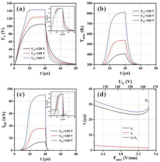
Figure 2.
Simulated temporal response of the gated ZnO nanowire field emitter under a single pulse with pulse width of 40 μs. (a) Uc versus t characteristics under different UG. The inset is the result of normalized Uc. (b) Tmax versus t characteristics under different UG. (c) IFE versus t characteristics under different UG. The inset is the result of normalized IFE, where t1 and t3 are defined as IFE arises to 90% and reduces to 10% of its maximal value. (d) The dependences of t1 and t3 on UG and the corresponding Fmax. The dot-dash line represents the critical field for thermal runaway.
The effect of pulse width on the minimum response time t1 + t3 and the corresponding UG as well as the maximum Tmax and Fmax during the pulse is presented in Figure 3, where Figure 3a is the result for t1 + t3 and Tmax; Figure 3b is the result for UG and Fmax. It is seen that when the pulse width is long enough for IFE to reach its steady state (larger than ~40 μs in our case), the minimum t1 + t3 as well as the optimal Tmax, UG, and Fmax are independent in terms of pulse widths, which are ~25 μs, ~710 K, 155 V, and ~5.16 V/nm, respectively. However, when the pulse width is below ~40 μs, the minimum t1 + t3 will reduce, and the optimal Tmax, UG, and Fmax will increase as the pulse width decreases. This is because when the pulse width is too short, IFE keeps increasing during the whole pulse. As mentioned above, IFE has a slower increasing rate at the beginning and end during its rising process. To minimize t1, the increasing rate for IFE at the end of the pulse needs to be as slow as possible (in other words, the operation time t2, which is equal to the time for IFE to increase from 90% of its maximum to the end of the pulse, needs to be as long as possible), which needs a larger UG as well as Fmax to reduce the delay for Uc. As a result, Tmax will also increase. It is worth pointing out that although a shorter pulse width induces a shorter response time, the operation time t2 will also reduce to nearly zero. Furthermore, when the pulse width is too short, Ug does not have enough time to rise to the applied UG. Therefore, this abnormal operation situation is not under consideration in the following section.
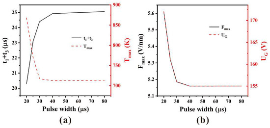
Figure 3.
Dependence of optimized temporal response of gated ZnO nanowire field emitter on pulse width. (a) Results of t1 + t3 and Tmax. (b) Results of Fmax and UG.
In the actual application, such as the application of the flat-panel X-ray source, the gated ZnO nanowire field emitter may need to work under continuous pulses. To investigate the influence of the self-heating effect in this case, its temporal response under continuous pulses with different UG is also simulated, for which the result with a pulse frequency of 25 kHz and UG of 164 V is shown in Figure 4. To maximize the duty ratio, we set the time for the off state (UG = 0 V) to be t3, which has been calculated from the single pulse case. Figure 4a shows the UG, Ug, and Uc versus t characteristics. It is clearly seen that under such a short time for the off state, both Ug and Uc cannot decrease to zero. However, for IFE, as shown in Figure 4c, it can be reduced to 10% of its maximum, which means that the device can be turned off. The underlying mechanism is due to the exponential relationship between IFE and Uc. From Figure 4c, the total response time t1 + t3 can be extracted as ~17.3 μs, which is shorter than that in the single pulse case (~27.4 μs) under the same UG with a pulse width of 40 μs. This is because during the short time of the off state, Tmax cannot cool down to room temperature, as shown in Figure 4b. As a result, R can remain at a lower value during the continuous pulses, which reduces the delay for Uc as well as IFE. Considering that the period of the pulses is 40 μs, t2 is ~22.7 μs, and the duty ratio for IFE can be calculated as ~57%, which is much smaller than that for the applied UG (~96%).
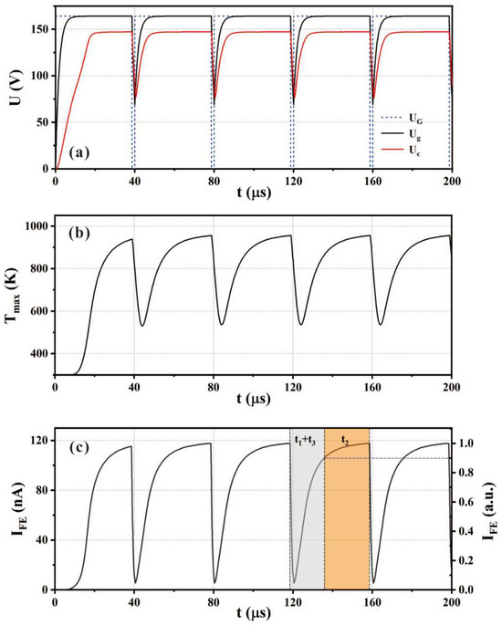
Figure 4.
Simulated temporal response of the gated ZnO nanowire field emitter under continuous pulses with frequency of 25 kHz and UG of 164 V. (a) UG, Ug, and Uc versus t characteristics. (b) Tmax versus t characteristics. (c) IFE versus t characteristics.
To further investigate the optimal response time under the continuous pulses, its dependence of UG has been simulated, which is shown in Figure 5a. Similar to the single pulse case, as shown in Figure 2d, t1 + t3 under continuous pulses also first decreases then increases with UG. The major difference between them is when UG is larger than the critical value for thermal runaway (164 V), the response time will rapidly increase in order to avoid the melting of the nanowire. Considering that the nanowire will not cool down to room temperature during each pulse, if the nanowire cannot reach a steady self-heating state under a given UG, the heat accumulation during each pulse can cause the nanowire to become thermal runaway at the end. Therefore, when UG is larger than 164 V, it requires a longer t3 to cool down the nanowire, which induces a rapid increase in t1 + t3. A comparison of the duty ratio for IFE and UG is also given in Figure 5b. It is seen that the maximum duty ratio for IFE is ~66% at UG of 155 V, which is smaller than that for UG (~96%). To increase the duty ratio for IFE, one needs to apply the continuous pulses with a lower frequency, which can increase the time of t2.
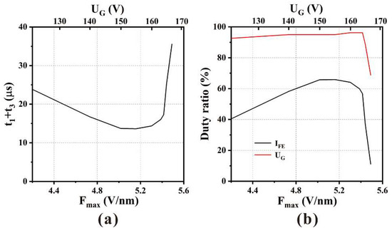
Figure 5.
Dependences of the temporal response of gated ZnO nanowire field emitter on UG and the corresponding Fmax under continuous pulses. (a) Result of t1 + t3. (b) Result of duty ratio for IFE and UG.
Finally, we discuss the optimization of nanowire resistance for improving the response speed. Assuming that R is reduced by one half, it can be realized by shortening L to L/2 (e.g., 2.5 μm), increasing r to (e.g., ~14.14 nm), increasing Nd to 2Nd (e.g., 4 × 1026 m−3), or decreasing Ed to Ed−kTln(2)/e (e.g., ~0.2121 eV), respectively. The optimized response time t1 + t3 and the corresponding Tmax for each case are calculated as shown in Table 1. Here, other parameters remain unchanged. It is seen that all the cases have a shorter t1 + t3 than that for the original nanowire (case 1) because of their reduced R. By shortening L (case 2), one can obtain the shortest t1 + t3 due to its smaller volume that causes a smaller heat capacity. Considering that it takes a shorter time to reach the same temperature, the optimal Tmax can be higher, which leads to a lower R and shorter t1 + t3. In comparison, we obtain a longer t1 + t3 than case 2 by increasing r (case 3) since it has a larger heat capacity, which results in a lower optimal Tmax as well as a higher R. Therefore, in the modification of the geometrical structure of nanowire, one needs to take into account the nanowire volume, which determines its heat capacity. To further reduce R, the nanowire resistivity needs to be reduced, for which the result can be seen in the comparison between cases 4 and 5. As mentioned before, a higher Tc benefits for a higher optimal Tmax, which leads to a shorter response time due to the lower R. For a better comparison, Tc for each case is also listed in Table 1. Considering that Tc increases with both Nd and Ed according to our previous work [26], a shorter t1 + t3 can be obtained by increasing Nd rather than decreasing Ed. Based on these results, the guideline that one needs to keep Tc as high as possible and the nanowire volume (heat capacity) as small as possible when reducing the nanowire resistance for improving the response speed is suggested. It is worth noting that although C is related to the geometrical structure of gate and nanowire, which can be different among cases 1, 2, and 3, this conclusion is still validated. This is because C will increase with r due to the larger tip surface area, which induces an even longer delay. While L reduces, the gate can be fabricated at the same distance with respect to the nanowire tip, which has a negligible influence on C. Considering that in the actual case of nanowires field emitter arrays, they inevitably have differences in their electrical properties and geometrical structures, which may cause deviation from the above conclusions, such as the relationship between response time and gate voltage, it is recommended that the model is validated by testing the pulsed field emission of individual nanowire, which can avoid the average effect.

Table 1.
Comparison on the temporal response of ZnO nanowire with different L, r, Nd, and Ed.
4. Conclusions
To summarize, a device model for a gated ZnO nanowire field emitter with consideration of charging and the self-heating effect has been established. Both simulations under single and continuous pulses show that the optimal field which minimizes the response time is below the critical field for thermal runaway, indicating that a higher critical temperature is favored for improving the response speed. Compared to the single pulse case, the continuous pulses case has a shorter response time because of the heat accumulation during each pulse, which keeps a low nanowire resistance. Possible ways to further improving its response speed are also discussed, which shows that the heat capacity as well as the critical temperature are two important factors in the optimization of nanowire resistance. All of these are important for the device design of a fast-response gated ZnO nanowire field emitter array.
Author Contributions
Conceptualization, J.C.; methodology, Y.C.; formal analysis, Y.C.; investigation, Y.C., C.W. and G.S.; data curation, Y.C.; writing—original draft preparation, Y.C.; writing—review and editing, S.D. and J.C.; supervision, J.C.; project administration, J.C.; funding acquisition, J.C. All authors have read and agreed to the published version of the manuscript.
Funding
This research was funded by the National Key Research and Development Program of China (Grant No. 2022YFA1204200), the Science and Technology Program of Guangzhou (Grant No. 202201011519), and the Science and Technology Planning Project of Guangdong Province (Grant No. 2023B1212060025).
Data Availability Statement
The data that support the findings of this study are available from the corresponding author upon reasonable request.
Conflicts of Interest
The authors declare no conflicts of interest.
References
- Choi, W.B.; Chung, D.S.; Kang, J.H.; Kim, H.Y.; Jin, Y.W.; Han, I.T.; Lee, Y.H.; Jung, J.E.; Lee, N.S.; Park, G.S.; et al. Fully sealed, high-brightness carbon-nanotube field-emission display. Appl. Phys. Lett. 1999, 75, 3129. [Google Scholar] [CrossRef]
- Zheng, K.; Shen, H.; Li, J.; Sun, D.; Chen, G.; Hou, K.; Li, C.; Lei, W. The fabrication and properties of field emission display based on ZnO tetrapod-liked nanostructure. Vacuum 2009, 83, 261–264. [Google Scholar] [CrossRef]
- Suzuki, M.; Kusunoki, T.; Sagawa, M.; Tsuji, K. Field-emission display based on nonformed MIM-cathode array. IEEE Trans. Electron Devices 2002, 49, 1005. [Google Scholar] [CrossRef]
- Robertson, J. Electron field emission from diamond and diamond-like carbon for field emission displays. Carbon 1999, 37, 759–763. [Google Scholar] [CrossRef]
- Jung, J.E.; Jin, Y.W.; Choi, J.H.; Park, Y.J.; Ko, T.Y.; Chung, D.S.; Kim, J.W.; Jang, J.E.; Cha, S.N.; Yi, W.K.; et al. Fabrication of triode-type field emission displays with high-density carbon-nanotube emitter arrays. Phys. B Condens. Matter 2002, 323, 71–77. [Google Scholar] [CrossRef]
- Nishino, H.; Yoshida, S.; Kojima, A.; Ikegami, N.; Tanaka, S.; Koshida, N.; Esashi, M. Fabrication of pierce-type nanocrystalline Si electron-emitter array for massively parallel electron beam lithography. Electr. Commun. Jpn. 2016, 99, 11–19. [Google Scholar] [CrossRef]
- Kirley, M.P.; Aloui, T.; Glass, J.T. Monolayer graphene-insulator-semiconductor emitter for large-area electron lithography. Appl. Phys. Lett. 2017, 110, 233109. [Google Scholar] [CrossRef]
- Teepen, T.F.; van Veen, A.H.; van’t Spijker, H.; Steenbrink, S.W.; van Zuuk, A.; Heerkens, C.T.; Wieland, M.J.; van Druten, N.J.; Kruit, P. Fabrication and characterization of p-type silicon field-emitter arrays for lithography. J. Vac. Sci. Technol. B 2005, 23, 359–369. [Google Scholar] [CrossRef]
- Minh, P.N.; Ono, T.; Sato, N.; Mimura, H.; Esashi, M. Microelectron field emitter array with focus lenses for multielectron beam lithography based on silicon on insulator wafer. J. Vac. Sci. Technol. B 2004, 22, 1273. [Google Scholar] [CrossRef]
- Ooki, S.; Ohshio, S.; Nishino, J.; Ohkawara, Y.; Ito, H.; Saitoh, H. X-ray source with cold emitter fabricated using ZnO conductive whiskers. Jpn. J. Appl. Phys. 2008, 47, 7303–7307. [Google Scholar] [CrossRef]
- Puett, C.; Inscoe, C.; Hartman, A.; Calliste, J.; Franceschi, D.K.; Lu, J.; Zhou, O.; Lee, Y.Z. An update on carbon nanotube-enabled X-ray sources for biomedical imaging. Wires Nanomed. Nanobiotechnol. 2018, 10, 1475. [Google Scholar] [CrossRef]
- Schwoebel, P.R. Field emission arrays for medical X-ray imaging. Appl. Phys. Lett. 2006, 88, 113902. [Google Scholar] [CrossRef]
- Zhang, J.; Yang, G.; Cheng, Y.; Gao, B.; Qiu, Q.; Lee, Y.Z.; Lu, J.P.; Zhou, O. Stationary scanning X-ray source based on carbon nanotube field emitters. Appl. Phys. Lett. 2005, 86, 184104. [Google Scholar] [CrossRef]
- Posada, C.M.; Grant, E.J.; Divan, R.; Sumant, A.V.; Rosenmann, D.; Stan, L.; Lee, H.K.; Castaño, C.H. Nitrogen incorporated ultrananocrystalline diamond based field emitter array for a flat-panel X-ray source. J. Appl. Phys. 2014, 115, 134506. [Google Scholar] [CrossRef]
- Busta, H.H.; Chen, J.M.; Shen, Z.; Jansen, K.; Rizkowski, S.; Matey, J.; Lanzillotto, A. Characterization of electron emitters for miniature X-ray sources. J. Vac. Sci. Technol. B 2003, 21, 344–349. [Google Scholar] [CrossRef]
- Yu, Y.Y.; Park, K.C. Fabrication of high quality X-ray source by gated vertically aligned carbon nanotube field emitters. J. Vac. Sci. Technol. B 2023, 41, 023203. [Google Scholar] [CrossRef]
- Bhattacharya, R.; Hay, R.; Cannon, M.; Karaulac, N.; Rughoobur, G.; Akinwande, A.I.; Browning, J. Demonstration of a silicon gated field emitter array based low frequency Colpitts oscillator at 400 °C. J. Vac. Sci. Technol. B 2023, 41, 023201. [Google Scholar] [CrossRef]
- Chen, Y.; Deng, S.; Xu, N.; Chen, J. Recent progress on ZnO nanowires cold cathode and its applications. Nanomaterials 2021, 11, 2150. [Google Scholar] [CrossRef] [PubMed]
- Lai, S.; Tang, X.; Liu, Y.; Mu, J.; Feng, Z.; Miao, K. X-ray high frequency pulse emission characteristic and application of CNT cold cathode X-ray source. Nanotechnology 2022, 33, 075201. [Google Scholar] [CrossRef]
- Lai, S.; Liu, Y.; Mu, J.; Feng, Z.; Miao, K.; Tang, X. X-ray ultrashort pulse emission characteristic of carbon nanotube cold cathode X-ray source by pulse driving mode. Vacuum 2023, 207, 111658. [Google Scholar] [CrossRef]
- Zhao, P.; Zhang, Y.; Tang, S.; Zhan, R.; She, J.; Chen, J.; Xu, N.; Deng, S. Effect of piezoresistive behavior on electron emission from individual silicon carbide nanowire. Nanomaterials 2019, 9, 981. [Google Scholar] [CrossRef]
- Huang, D.; Chen, Y.; Wang, C.; She, J.; Deng, S.; Chen, J. Improving the response speed of an active-current controlled field emitter arrays by modifying the controlled current. IEEE T. Electron Dev. 2022, 69, 5895–5899. [Google Scholar] [CrossRef]
- Liao, Q.; Zhang, Y.; Qi, J.; Huang, Y.; Xia, L.; Gao, Z.; Gu, Y. Plasma-induced field emission and plasma expansion of carbon nanotube cathodes. J. Phys. D Appl. Phys. 2007, 40, 3456–3460. [Google Scholar] [CrossRef]
- Liao, Q.; Yang, Y.; Xia, L.; Qi, J.; Zhang, Y.; Huang, Y.; Qin, Z. High intensity, plasma-induced emission from large area ZnO nanorod array cathodes. Phys. Plasmas 2008, 15, 114505. [Google Scholar] [CrossRef]
- Xun, T.; Zhao, X.L.; Li, G.Y.; Hu, T.J.; Yang, J.; Yang, H.W.; Zhang, J.D. High-current, pulsed electron beam sources with SiC nanowire cathodes. Vacuum 2016, 125, 81–84. [Google Scholar] [CrossRef]
- Chen, Y.; Luo, S.; Cao, X.; Li, Y.; She, J.; Deng, S.; Chen, J. Stable heating above 900 K in the field emission of ZnO nanowires: Mechanism for achieving high current in large scale field emitter arrays. Adv. Electron. Mater. 2020, 6, 2000624. [Google Scholar] [CrossRef]
- Semet, V.; Binh, V.T.; Pauporté, T.; Joulaud, L.; Vermersch, F.J. Field emission behavior of vertically aligned ZnO nanowire planar cathodes. J. Appl. Phys. 2011, 109, 054301. [Google Scholar] [CrossRef]
Disclaimer/Publisher’s Note: The statements, opinions and data contained in all publications are solely those of the individual author(s) and contributor(s) and not of MDPI and/or the editor(s). MDPI and/or the editor(s) disclaim responsibility for any injury to people or property resulting from any ideas, methods, instructions or products referred to in the content. |
© 2024 by the authors. Licensee MDPI, Basel, Switzerland. This article is an open access article distributed under the terms and conditions of the Creative Commons Attribution (CC BY) license (https://creativecommons.org/licenses/by/4.0/).