Abstract
This paper describes an analysis of power supply rejection and noise improvement techniques for an envelope-tracking power amplifier. Although the envelope-tracking technique improves efficiency, its power supply rejection ratio is much lower than that of average power tracking or a fixed-supply power amplifier. In FDD systems with the envelope-tracking technique, the low power supply rejection ratio generates much output noise in the RX band and degrades the receiver’s sensitivity. An SM is designed by using a 130 nm CMOS process, and the chip die area is 2 × 2 mm2 with a 25-pin wafer-level chip-scale package. The designed SM achieved peak efficiencies of 78–83% for LTE signals with a 5.8 dB PAPR and various channel bandwidths. For the low-output-noise-supply modulator, noise reduction techniques using resonant-frequency tuning and a notch filter are employed, and the measured results show maximum 1.8/5/5.3/3.8/3 dB noise reduction in LTE bands B17/B5/B2/B3/B7, respectively.
1. Introduction
Wireless communication systems have a complex modulation scheme and a high peak-to-average power ratio (PAPR) to maximize data throughput with limited spectrum resources. Envelope tracking (ET) is an essential efficiency improvement technique for a power amplifier (PA) to achieve a longer battery lifetime in mobile handsets. An ET PA has much better efficiency than average power tracking (APT) or a battery-connected PA undergoing saturated operation under a modulated supply voltage. However, an ET PA has many difficulties in terms of commercialization and mass production. Receiver sensitivity due to the PA noise in the receiver band is one of the most difficult issues in ET PAs in a frequency division duplex (FDD) system because of the simultaneous operations of transmitting and receiving, as shown in Figure 1. In an APT or a battery-connected PA, the upconverted supply noise is not a problem because the supply noise can easily be suppressed by a large decoupling capacitor, and the mixing gains of the RF input and supply noise are small. Typically, PA noise from RFIC noise is larger than that from supply modulator (SM) [1,2,3,4,5,6,7,8] noise in an APT PA. In an ET PA, this relation is reversed because the upconverted supply noise is much larger than in APT due to its larger supply noise and mixing gain. The supply noise suppression is limited because the large decoupling capacitor is not allowed to provide a large-bandwidth envelope signal. The mixing gain of ET is much larger than that of APT because the PA operates in a saturated region.
Figure 1.
RX-band noise transfer from ET PA in FDD system.
In [9], the power supply rejection ratio (PSRR) of a PA is analyzed to figure out the spectral regrowth and mask violation of a 2G system. However, the analysis is for PA operation in a linear region under a fixed supply voltage, not in a saturation region under a modulated supply voltage for ET operation. In Section 2, the receiver sensitivity and PSRR of a PA in a linear region as well as a saturation region are analyzed to specify the requirements of SM noise. In [10,11,12,13], some noise reduction methods for a supply modulator are suggested. The reduced switching frequency in [10] improves noise performance, but it degrades efficiency. The methods in [11,12,13] are very effective for low levels of noise with little or no efficiency degradation. In Section 3, noise reduction techniques based on the above references and a notch filter are described for further improvement in SM noise. In Section 4, the measured output noise performances of a supply modulator are presented.
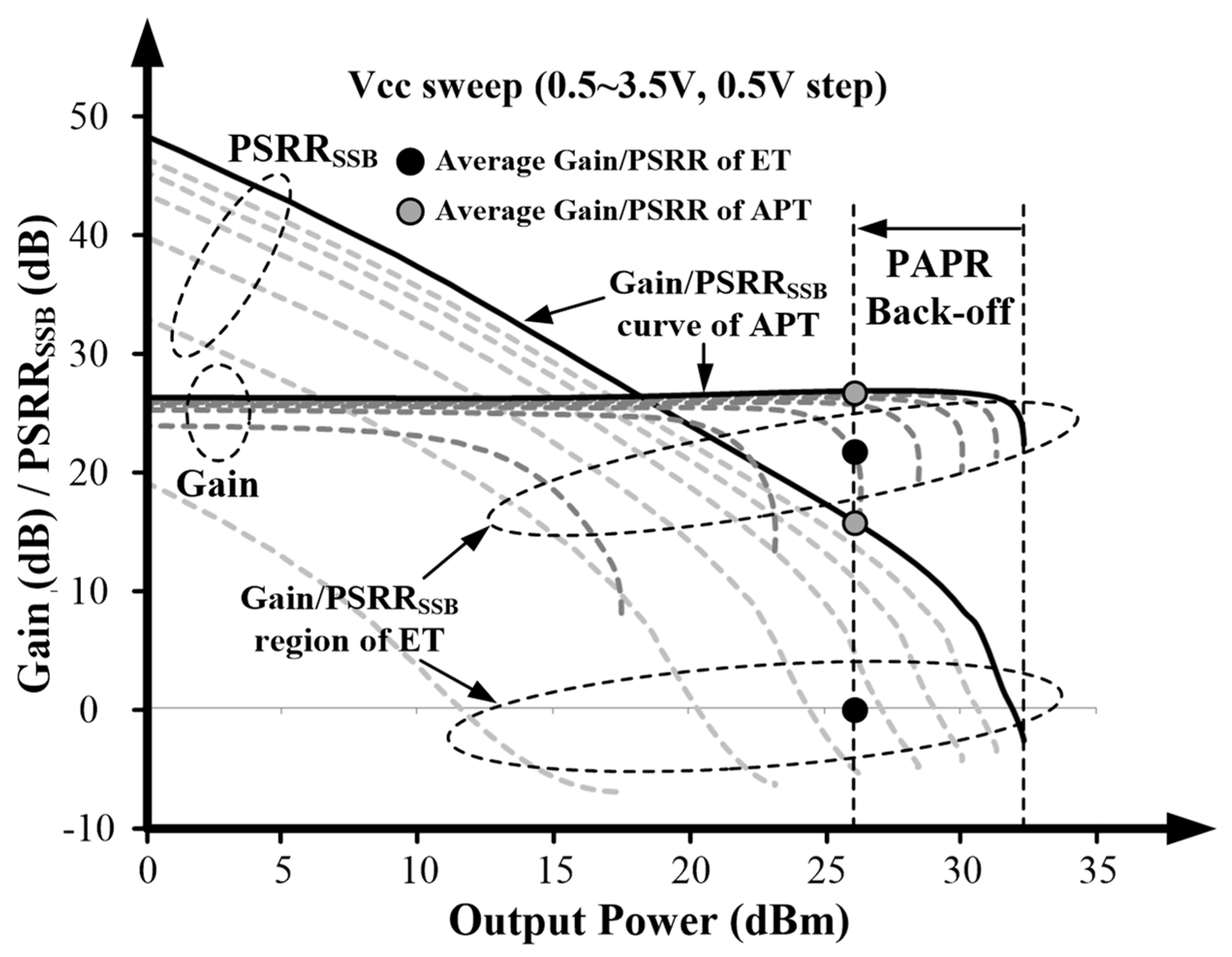
2. Sensitivity and PSRR of Power Amplifier
In an FDD system with an ET PA, the receiver’s sensitivity is degraded by the PA output noise (PPAN) from the SM noise (PSMN), as shown in Figure 1. The receiver sensitivity is the minimum detectable input power (Pin_min_dBm), and it can be defined in the following equations:
where BW is the signal bandwidth in Hz, NF is the noise figure of the receiver path, SNR is the required signal-to-noise ratio of the system, and AttenDP is the attenuation of the duplexer. If the specification for sensitivity degradation is lower than 0.4 dB and the attenuation of the duplexer is 45 dB, the required PA noise is under −139 dBm/Hz. The required SM noise is determined from the required PA noise and PSRR of the PA (PSRRPA), as given in (2). The PSRR of the PA can be defined in the following equations:
where ωn is the TRX offset frequency of the FDD system, ω0 is the RF carrier center frequency, ΔVCC_ωn is the supply noise amplitude at ωn, and ΔVPAOUT_ωo±ωn is the RF output noise amplitude at ωo ± ωn. Because the RF output noise due to the supply noise is located at a positive and negative offset frequency of ωn, the single-sideband PSRR (PSRRSSB) is a meaningful value that can be used to express RX-band noise. In this paper, the noise amplitude and noise power are calculated and measured with a 50-Ohm load impedance for convenience.
Figure 2 shows the PSRR difference between the linear region and saturated region of the PA. In the linear region, the PA has a high PSRR because it has little gain variation due to the supply voltage change. In the saturation region, the PA has a much decreased PSRR due to the large gain variation over the supply voltage. To quantify and compare the PSRR of APT and ET, a mathematical PA model [14] is used to simulate gain and the PSRR at various supply voltages and input/output power values.
Figure 2.
PSRR of PA in linear and saturated regions near P1dB.
Figure 3 shows the simulation results, and the simulated PSRR is well matched at a low frequency offset (tens of MHz) from the carrier frequency. For a large frequency offset (larger than 100 MHz), the PSRR increased due to the reduced gain caused by the limited PA bandwidth. In APT mode under 3.5 V, the PSRRSSB range is from −3 dB to over 50 dB. The average PSRRSSB of APT is about 15 dB for the LTE signal, with a 6 dB PAPR. In ET mode, the PSRRSSB curve is located around 0 dB, and it is changed by an envelope-shaping function and the saturation level. The average PSRRSSB of ET is about 0 dB for LTE, and its slope is about −4 dB per 1 dB of output power. From this result and the required PA output noise, the required SM noise is determined to be about −134 dBm/Hz. If there is a margin in the SM noise, the ET PA system has many advantages such as better sensitivity, reduced requirement for duplexer attenuation, and higher PA efficiency due to having more saturated ET operation with a reduced PSRR. Therefore, noise reduction techniques are essential in SM design.
Figure 3.
Simulated gain and PSRRSSB curves of APT and ET.
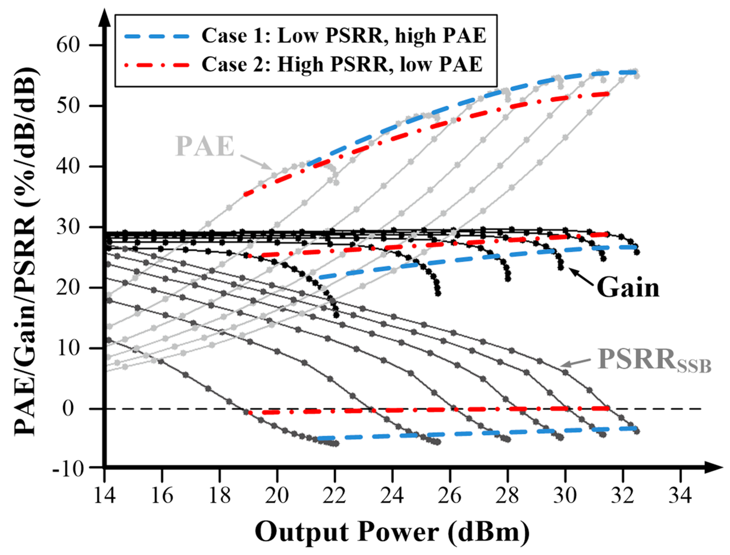
3. Trade-Off Between Efficiency and RX-Band Noise
In the ET PA, the operating point of the PA is an important factor in determining efficiency and RX-band noise. If the PSRR is not an important factor (TDD system, good duplexer isolation, good SM noise), case 1 in Figure 4, having the highest PAE (Power-Added Efficiency) and a poor PSRRSSB, is a suitable operating curve. If the PSRR is an important factor (FDD system, poor duplexer isolation, poor SM noise), case 2, having a good PSRRSSB and reduced PAE, is a suitable operating curve. Figure 5 shows the characteristics of the PA according to the saturation level in ET operation. As shown in this figure, the efficiency of the PA and RX-band noise (or PSRR) are in a trade-off relationship with each other, and the operating curve should be carefully determined by the system requirements.
Figure 4.
Simulated PAE, gain, and calculated PSRRSSB curves of PA at each supply voltage (1 V to 3.5 V with 0.5 V step).
Figure 5.
Average PAE, gain, output power, and PSRRSSB according to saturation level in ET operation.
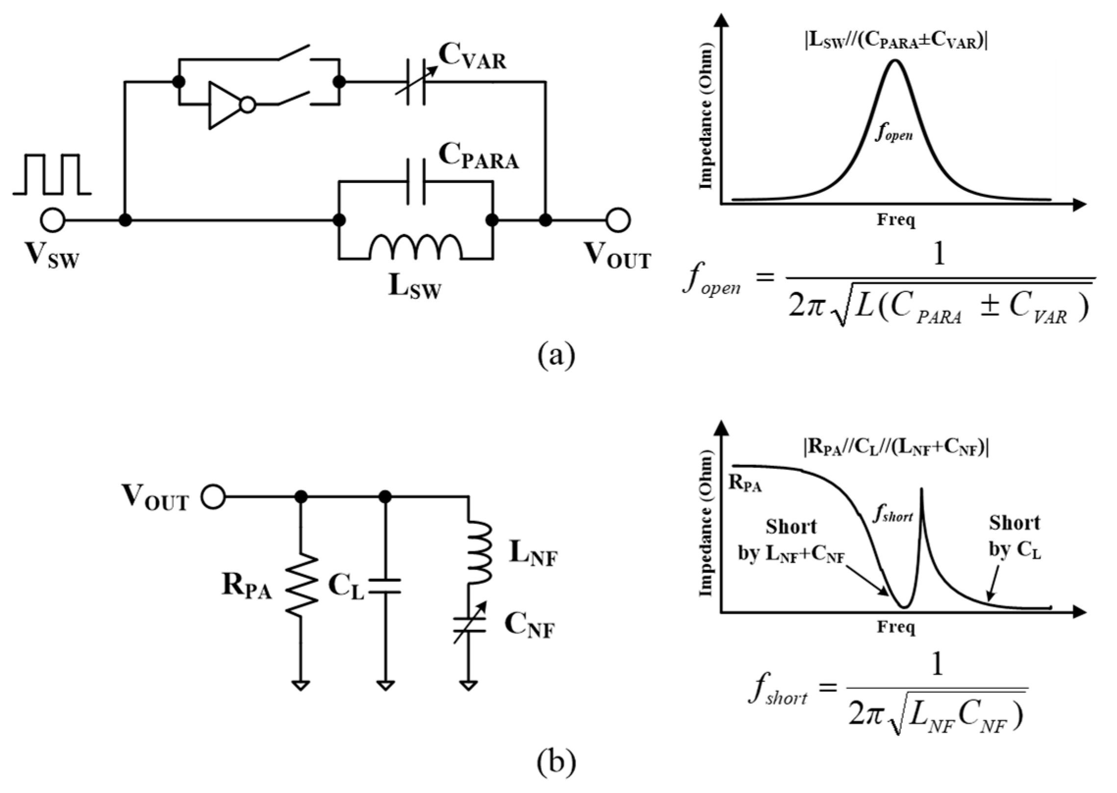
4. Low-Noise-Supply Modulator Design
Figure 6 shows a block diagram of the supply modulator. RFT is a noise-blocking technique that blocks noise from the VSW node to the VOUT node. CLs and notch filters (LNF and CNF) are noise-removing techniques used at the VOUT node. In APT operation, the supply noise is easily suppressed by the very low impedance of a large decoupling capacitor. In ET operation, the wideband linear amplifier acts like a large decoupling capacitor. However, the output impedance is increased as frequency increases due to decreased loop gain. In [11], low output impedance is achieved with a linear amplifier at a low frequency and a load capacitor (a few nF) at a high frequency. The voltage-sensing negative feedback loop of the linear amplifier lowers the SM output impedance within the unit loop bandwidth, so the linear amplifier can provide low output impedance as a voltage source. Figure 7 shows the SM output noise open-loop model. In this paper, a load capacitor, resonant-frequency tuning (RFT), and a notch filter are used for noise reduction.
Figure 6.
Block diagram of the hybrid switching supply modulator.
Figure 7.
SM output open-loop noise model and noise contribution depending on frequency offset.
Figure 8a shows an inductor (LSW) of a switching amplifier with its parasitic capacitor (CPARA) and a variable capacitor (CVAR), which are integrated into the IC. The switching noise at the VSW node is blocked at a certain frequency (fopen) by the high impedance of the parallel LSW and the equivalent capacitance of CPARA±CVAR. Figure 8b shows the equivalent load resistance of the PA, CL, and notch filter. The PA has a low impedance at a certain frequency (fshort) due to the notch filter and at a high frequency due to CL. The optimized noise performance for each band is possible by controlling the resonant frequencies of fopen and fshort according to the separation between the uplink and downlink frequencies.
Figure 8.
Proposed noise reduction techniques: (a) resonant-frequency tuning (RFT); (b) notch filter.
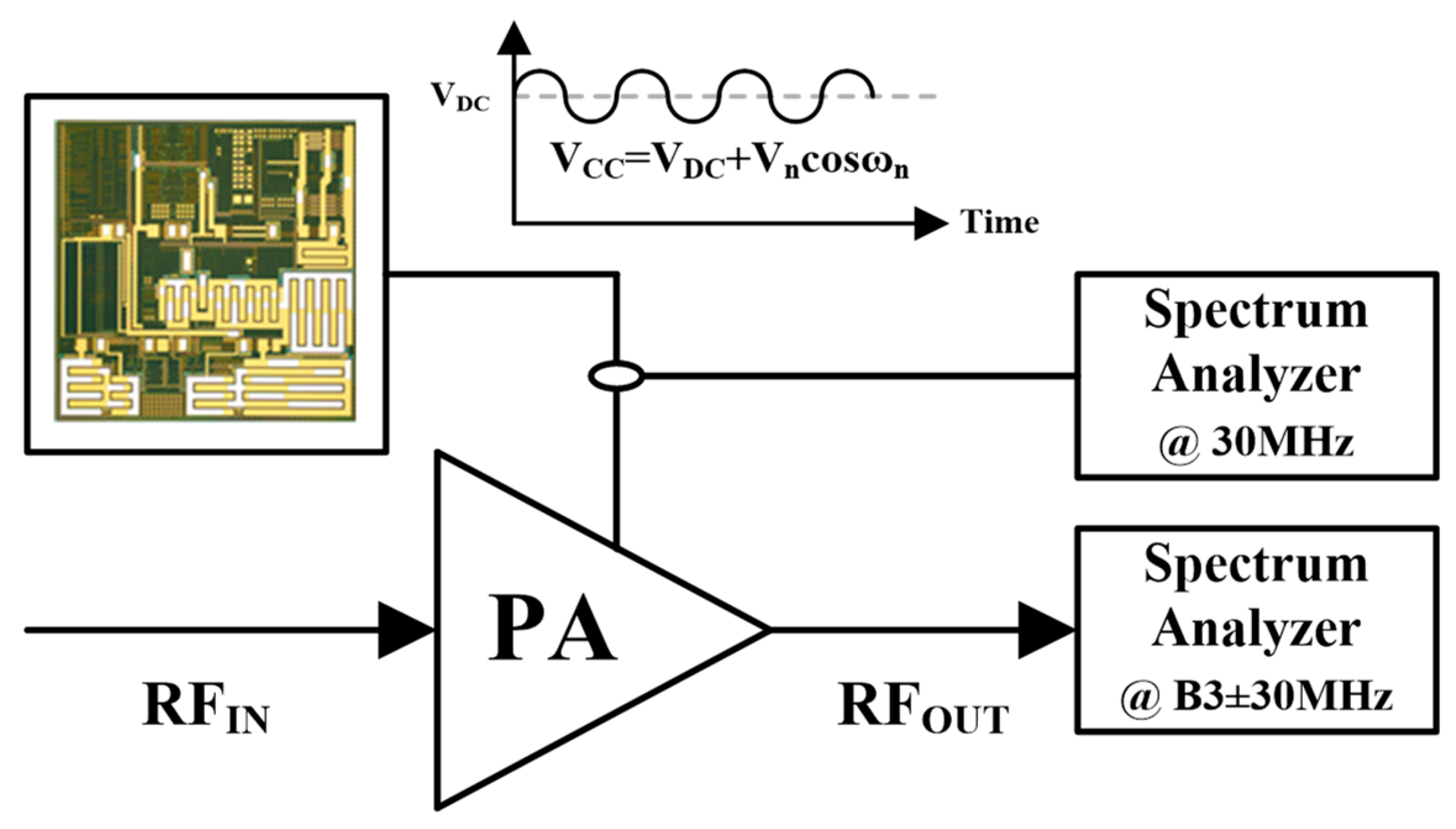
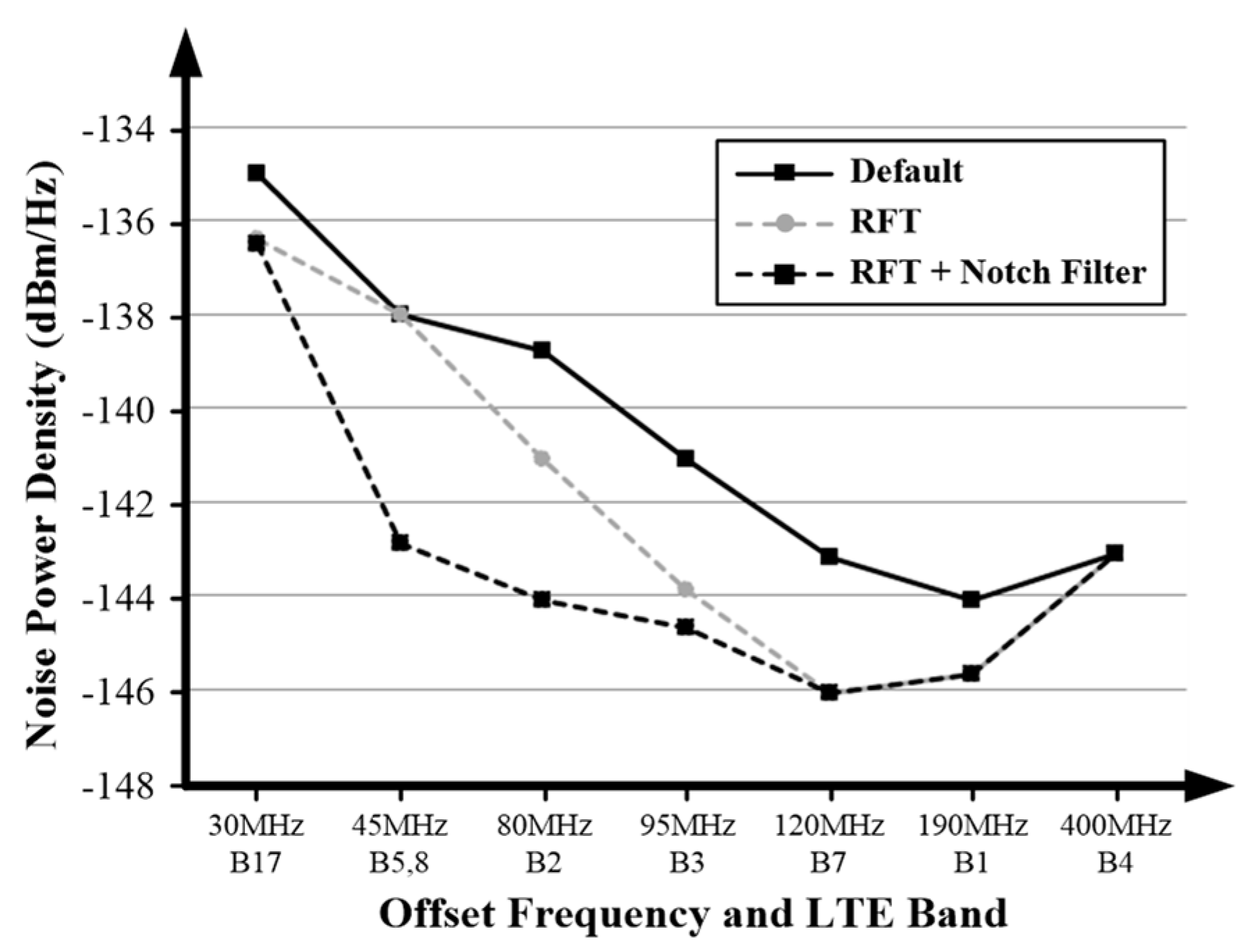
5. Measurement Results
In the RX-band noise measurement, the frequency of interest and number of resource blocks for the signal are different because each LTE band has a different TX-RX frequency separation and channel bandwidth. Our measurement condition is based on the reference sensitivity QPSK PREFSENS (Table 7.3.1-1 in [15]), and the worst noise performance in Table 1 occurs at the maximum channel bandwidth.
Table 1.
Performance comparison.
The SM is designed by using a 130 nm CMOS process, and the chip die area is 2 × 2 mm2 with a 25-pin wafer-level chip-scale package, and Figure 9 shows the measurement setup with a chip photograph. It delivers envelope supply voltages with peak efficiencies of 78–83% for LTE signals with a 5.8 dB PAPR and various channel bandwidths. Figure 10 shows the measured output noise power of the supply modulator. In the default case, only the load capacitor (CL) is attached to the equivalent load resistance (RPA). In the case of RFT, it has no effect at 45 MHz for B5 and B8 because the default resonant frequency (fopen) of the power inductor used (LSW//CPAPR) is around 45 MHz. At 30 MHz for B17, CVAR is added to CPARA to lower fopen, and this leads to a 1.4 dB reduction in noise. For other frequencies from 80 MHz to 400 MHz, the inverter makes CVAR negative, and the noise is suppressed by the increased fopen. The notch filter improves noise performance from 45 MHz to 95 MHz. At high frequencies (≥95 MHz), CL has enough suppression without the notch filter. At 30 MHz, the notch filter is not used because it degrades the loop stability of the linear amplifier.
Figure 9.
PSRR measurement setup and chip photograph.
Figure 10.
Measured output noise of the designed supply modulator in the cases of reference sensitivity QPSK PREFSENS (Table 7.3.1-1 in [5]) for each LTE band.
6. Conclusions
Power supply rejection for the ET PA and receiver sensitivity degradation due to PA noise were analyzed, and these show the importance of the output noise performance of the supply modulator. The low output noise is made possible by noise blocking and generating a low output impedance. The RFT blocks switching noise transfer between the power inductor of the switching amplifier. The notch filter and load capacitance achieve low output impedance and remove the output noise. The measured results show a maximum of 1.8/5/5.3/3.8/3 dB noise reduction in the LTE B17/B5/B2/B3/B7 RX band due to the RFT and notch filter, respectively. The designed SM achieved peak efficiencies of 78–83% for LTE signals with a 5.8 dB PAPR with various channel bandwidths.
Funding
This study was conducted with support from institute information & communications technology planning & evaluation from the government (Ministry of Science and ICT) in 2024. (No. RS-2024-00395702, Development of Envelope Tracking PAM for Sub-6GHz Massive MIMO Supported Base Stations).
Data Availability Statement
Data are contained within the article.
Conflicts of Interest
The author declares no conflict of interest.
References
- Paek, J.S.; Kim, D.; Bang, J.S.; Baek, J.; Choi, J.; Nomiyama, T.; Kang, I. An 88%-Efficiency Supply Modulator Achieving 1.08 μs/V Fast Transition and 100 MHz Envelope-Tracking Bandwidth for 5G New Radio RF Power Amplifier. In Proceedings of the 2019 IEEE International Solid-State Circuits Conference-(ISSCC), San Francisco, CA, USA, 17–21 February 2019; pp. 238–239. [Google Scholar]
- Arno, P.; Thomas, M.; Molata, V.; Jerabek, T. Envelope Modulator for Multimode Transmitters with AC-Coupled Multilevel Regulators. In Proceedings of the 2014 IEEE International Solid-State Circuits Conference Digest of Technical Papers (ISSCC), San Francisco, CA, USA, 9–13 February 2014; pp. 296–297. [Google Scholar]
- Riehl, P.; Fowers, P.; Hong, H.; Ashburn, M. An AC-coupled hybrid envelope modulator for HSUPA transmitters with 80% Modulator. In Proceedings of the 2013 IEEE International Solid-State Circuits Conference Digest of Technical Papers, San Francisco, CA, USA, 17–21 February 2013; pp. 364–365. [Google Scholar]
- Hassan, M.; Larson, L.E.; Leung, W.; Kimball, D.F.; Asbeck, P.M. A wideband CMOS/GaAs HBT envelope tracking power amplifier for 4G LTE mobile terminal applications. IEEE Trans. Microw. Theory Tech. 2012, 60, 1321–1330. [Google Scholar] [CrossRef]
- Paek, J.S.; Kim, W.; Kang, S.; Lee, J.; Pyo, S.; Cho, Y.; Hur, Y. A 5G New Radio SAW-less RF Transmitter with a 100MHz Envelope Tracking HPUE n77 Power Amplifier Module. In Proceedings of the 2021 Symposium on VLSI Circuits, Kyoto, Japan, 13–19 June 2021; pp. 1–2. [Google Scholar]
- Ho, C.-Y.; Lin, S.-M.; Meng, C.-H.; Hong, H.-P.; Yan, S.-H.; Kuo, T.-H.; Peng, C.-S.; Hsiao, C.-H.; Chen, H.-H.; Sung, D.-W.; et al. An 87.1% Efficiency RF-PA Envelope-Tracking Modulator for 80 MHz LTE-Advanced Transmitter and 31 dBm PA Output Power for HPUE in 0.153 μm CMOS. In Proceedings of the 2018 IEEE International Solid-State Circuits Conference (ISSCC), San Francisco, CA, USA, 11–15 February 2018; pp. 432–433. [Google Scholar]
- Wang, F.; Yang, A.H.; Kimball, D.F.; Larson, L.E.; Asbeck, P.M. Design of wide-bandwidth envelope-tracking power amplifiers for OFDM applications. IEEE Trans. Microw. Theory Tech. 2005, 53, 1244–1255. [Google Scholar] [CrossRef]
- Hoversten, J.; Schafer, S.; Roberg, M.; Norris, M.; Maksimovic, D.; Popovic, Z. Codesign of PA, Supply, and Signal Processing for Linear Supply-Modulated RF Transmitters. IEEE Trans. Microw. Theory Tech. 2012, 60, 2010–2020. [Google Scholar] [CrossRef]
- Stauth, J.T.; Sanders, S.R. Power supply rejection for RF amplifiers: Theory and measurements. IEEE Trans. Microw. Theory Techn. 2007, 55, 2043–2052. [Google Scholar] [CrossRef]
- Honda, Y.; Yokota, Y.; Goto, N.; Matsuno, N.; Saito, Y. A wide supply voltage and low-Rx noise envelope tracking supply modulator IC for LTE handset power amplifiers. In Proceedings of the 2012 7th European Microwave Integrated Circuit Conference, Amsterdam, The Netherlands, 29–30 October 2012; pp. 1253–1256. [Google Scholar]
- Kim, J.; Kim, D.; Cho, Y.; Kang, D.; Park, B.; Moon, K.; Kim, B. Analysis of far-out spurious noise and its reduction in envelope-tracking power amplifier. IEEE Trans. Microw. Theory Techn. 2015, 63, 4072–4082. [Google Scholar] [CrossRef]
- Lee, S.C.; Paek, J.S.; Jung, J.H.; Youn, Y.S.; Lee, S.J.; Cho, M.S.; Kang, I. A hybrid supply modulator with 10 dB ET operation dynamic range achieving a PAE of 42.6% at 27.0 dBm PA output power. In Proceedings of the 2015 IEEE International Solid-State Circuits Conference—(ISSCC) Digest of Technical Papers, San Francisco, CA, USA, 22–26 February 2015; pp. 42–43. [Google Scholar]
- Paek, J.-S.; Youn, Y.-S.; Choi, J.-H.; Kim, D.-S.; Jing, J.-H.; Choo, Y.-H.; Lee, S.-J.; Lee, S.-C.; Cho, T.B.; Kang, I.-Y. An RF-PA supply modulator achieving 83% efficiency and −136dBm/Hz noise for LTE-40MHz and GSM 35dBm applications. In Proceedings of the 2016 IEEE International Solid-State Circuits Conference (ISSCC), San Francisco, CA, USA, 31 January–4 February 2016; pp. 354–355. [Google Scholar]
- Kim, J.; Kim, D.; Cho, Y.; Kang, D.; Park, B.; Moon, K.; Kim, B. Analysis of envelope-tracking power amplifier using mathematical modeling. IEEE Trans. Microw. Theory Techn. 2014, 62, 1352–1362. [Google Scholar] [CrossRef]
- 3rd Generation Partnership Project; Technical Specification Group Radio Access Network; Evolved Universal Terrestrial Radio Access (E-UTRA); User Equipment (UE) Radio Transmission and Reception (3GPP TS 36.101 version 12.5.0 Release 12), 3GPP. 2014. Available online: https://portal.3gpp.org/desktopmodules/Specifications/SpecificationDetails.aspx?specificationId=2411 (accessed on 10 November 2024).
Disclaimer/Publisher’s Note: The statements, opinions and data contained in all publications are solely those of the individual author(s) and contributor(s) and not of MDPI and/or the editor(s). MDPI and/or the editor(s) disclaim responsibility for any injury to people or property resulting from any ideas, methods, instructions or products referred to in the content. |
© 2024 by the author. Licensee MDPI, Basel, Switzerland. This article is an open access article distributed under the terms and conditions of the Creative Commons Attribution (CC BY) license (https://creativecommons.org/licenses/by/4.0/).