Abstract
This paper proposes a 12-bit SAR ADC capable of calibrating a split capacitor using a binary search technique for bio-signal processing applications. The proposed SAR ADC employs a calibration logic circuit to calibrate a split capacitor vulnerable to process variations and mismatches. The proposed foreground calibration process involves four iterations through the binary search algorithm. In this manner, the calibration speed can be increased by up to 3.75 times compared with that of the linear search calibration. The proposed SAR ADC was implemented with a CMOS 28 nm 1-poly 8-metal process. The effective layout, excluding bonding pads, occupied 939 × 450 m. Measurement results illustrated a power consumption of 30.7 W (analog power: 16.1 W and digital power: 14.6 W), INL/DNL of −1.8/1.7 LSB, and −0.7/0.7 LSB, respectively, ENoB of 10.3-bit, and a FoM of 53.7 fJ/step.
1. Introduction
Wearable devices are receiving significant attention. Research on low-power, high-resolution ADCs (Analog Digital Converters) is currently underway for bio-signal processing.
Bio-signals consist of EEG (electroencephalography), ECG (electrocardiography), and EMG (electromyography) signals. EEG, ECG, and EMG signals have a bandwidth of 0.1–100 Hz, 0.05–500 Hz, and 10 Hz–5 kHz, respectively. In addition, the voltage range of the bio-signals is small (V 100 mV) [1]. Due to the frequency and voltage range of EEG, EMG and ECG signals, the ADC should maintain a minimum 8-bit resolution and a 10 kHz sampling rate specification to be able to handle bio-signal processing. And this ADC should consume minimal power for portability and for embedded application in other electronic systems, which inherently results in the adaption of the SAR (Successive Approximation Register) ADC.
Recent research has been focused on developing low-power ADCs [2,3,4,5,6,7,8,9,10,11,12,13,14,15,16,17,18,19,20,21,22,23,24]. In addition, when designing a low-power ADC, foreground and background calibration are performed to improve performance [7,8,12]. Foreground calibration is performed after bit conversion. Foreground calibration consumes less power with a slow sampling rate due to the calibration phase. On the other hand, background calibration conducts calibration and bit conversion at the same time. Background calibration offers a faster sampling rate than foreground calibration, but its calibration logic circuit is complex and consumes a lot of power. TS SS (Two-Step Single-Slope) ADCs are also being studied because of thier low power and high resolution [8]. A TS SS ADC uses a linear search algorithm based on a digital counter in bit conversion, which results in a slow sampling rate with low power consumption. Since it employs a digital counter and a ramp generator, this ADC is suitable for bio-signal processing requiring minimal power consumption and high resolution. The ramp output of a TS SS ADC is applied to the R-DAC (Resistor Digital to Analog Converter), and the output of the R-DAC is divided into two parts: coarse and fine conversions. Employment of an R-DAC causes process variation and high power consumption. Coarse conversion of the TS SS ADC operates at the time of bit conversion, and the fine conversion follows the coarse conversion. The coarse conversion has a higher weight factor of R-DAC than that of the fine conversion.
The authors of [7] performed background calibration on a split capacitor by adjusting a 7-bit assist DAC in the LSB (Least Significant Bit) part of the C-DAC (Capacitor Digital to Analog Converter). A 7-bit assist DAC in [7] is connected to the output of the main C-DAC. The error detection register inside the ADC detects an error in the voltage generated by the mismatch. After that, the value stored in the error detection register is reflected by the 7-bit assist DAC. The error value is reflected through a feedback loop in the output of the C-DAC, canceling the error in the C-DAC. This allows the output of the C-DAC to be corrected. However, the ADC in [7] suffers from high INL (Integral Non-Linearity) and low ENoB (Effective Number of Bit). Likewise, 1.5-bit redundancy in [8] is designed so that the weight of the bits is duplicated. A calibration signal is generated from the duplicated bits and is applied to the digital calibration logic, which allows the DAC to offset the error. The ADC employing 1.5-bit redundancy exhibits low power, but poor INL and ENoB. Through calibration, the output waveform of the lamp is adjusted so that the output of the DAC approaches the ideal slope. However, paper [8] suffered from poor INL and papers [7,8] had slow sampling rates. Especially, ref. [8] consumed 62 W and had an ENoB of 9.8-bit.
The main idea of [9] is to present a practical low-power solution through a low-power sensor interface design in RFID (Radio-Frequency Identification) applications, thereby improving sensor data collection and performance of RFID systems. However, this research suffered from a low sampling speed of 6.25 kS/s and a low ENoB of 9.7-bit. Further, the main idea of [10] is to provide a hybrid design tool for automating and optimizing the design of SAR ADC in IoT applications. The ADC in [11] encloses a charge pump circuit and a phase frequency detector to eliminate the offset of the comparator. A phase difference occurs in the two differential outputs of the comparator due to the offset error of the comparator. This phase difference is detected by the phase frequency detector and the output of the phase frequency detector is applied to the charge pump. The output value of the charge pump is fed back to the comparator, eliminating the offset of the comparator. This calibration technique is valid for a high sampling rate, but suffers from high INL and low ENoB. Overall, refs. [9,10,11] without a calibration circuit showed low ENoB and poor INL. In [12,25], the calibration circuit employed a linear search technique where the size of the split capacitor is sequentially increased. However, the linear search technique requires a considerable amount of calibration time to find the proper split capacitor that matches the operating conditions. Additionally, if an incorrect split capacitor is calibrated due to comparator offset and external noise, the performance of the SAR ADC is further deteriorated. In [12], an ENoB of 11.5-bit, DNL (Differential Non-Linearity)/INL of ±1 LSB and −2.6/2.1 LSB, and FoM (Figure of Merit) of 155 fJ/step was achieved, indicating poor linearity and FoM performance.
Overall, the ADC presented in [7,8,9,10,11] showed high INL, slow sampling rates, and low ENoB. ADCs employed by bio-signal processors and wearable devices should be capable of providing low INL, a reasonably fast sampling rate (>10 kHz), and high ENoB. There is a need for different design techniques to provide low INL, a fast sampling rate, and high ENoB to ADCs processing EEG, ECG, and EMG bio-signals.
This paper presents a 12-bit SAR ADC that employs a binary search algorithm-based split capacitor calibration technique. The proposed SAR ADC uses the binary search technique four times to calibrate the split capacitor, enabling faster and more accurate calibration compared with the conventional linear search method. The architecture and the proposed design methodology is discussed in Section 2, measurement results are presented in Section 3, and conclusions are drawn in Section 4.
2. Materials and Methods
A block diagram of the proposed 12-bit SAR ADC with split capacitor foreground calibration based on a binary search algorithm is shown in Figure 1. The proposed ADC is composed of a C-DAC in differential mode, calibration switch control logic, a comparator connected to a pre-amplifier, 12-bit SAR logic, a reset generator, and an output register with the calibration split capacitor array. The calibration switch control logic contains the calibration logic and 2-CLK (Clock Signal) divider. The P and N nodes represent the upper and lower C-DAC, respectively.
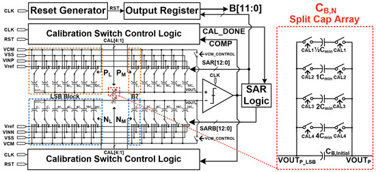
Figure 1.
Block diagram of the proposed 12-bit SAR ADC with split capacitor calibration based on a binary search algorithm.
Employment of a C-DAC is necessary for low-power application of the proposed 12-bit SAR ADC because it takes advantage of low-power consumption due to no dc current flow and low speed because of the charging and discharging capacitor array. In order to further reduce power consumption of the proposed ADC, total capacitance of the C-DAC should be minimized because power consumption is proportional to total capacitance of the C-DAC. Instead of utilizing the conventional binary weighted capacitor array in the C-DAC, a 6-bit MSB C-DAC and 6-bit LSB C-DAC with a split capacitor for foreground calibration, as shown in Figure 1, is employed to minimize total capacitance of the C-DAC in the proposed ADC. There are two types of calibration algorithm applicable to a split capacitor array, namely linear search algorithm and binary search algorithm. The plot shown in Figure 2 compares a number of capacitors from the binary search technique and that of the linear search technique as a function of the calibration cycle, where each cycle requires two CLKs. Calibration employing the linear search technique is capable of adding a split capacitor of 2 for a 4-cycle. On the other hand, employing the proposed binary search technique, a split capacitor of up to 15/2 may be added for a 4-cycle. A total of 15 calibration cycles are required to add a split capacitor of 15/2 with the linear search technique, so that it takes about 3.75 times longer than the binary search method. Therefore, the binary search method reduces the time required for foreground calibration, thereby increasing the sampling rate. As a result, the proposed ADC employs the binary search calibration algorithm.
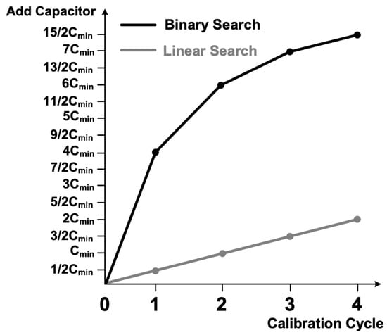
Figure 2.
Comparison of total calibration capacitors of binary and linear search techniques.
The split capacitor array consists of a split capacitor of , , , and , where is the minimum unit capacitor (2fF) of the split capacitor array, as in Figure 1. The split capacitor array with calibration signal, CAL[4:1], is placed between the MSB and LSB blocks of the C-DAC.
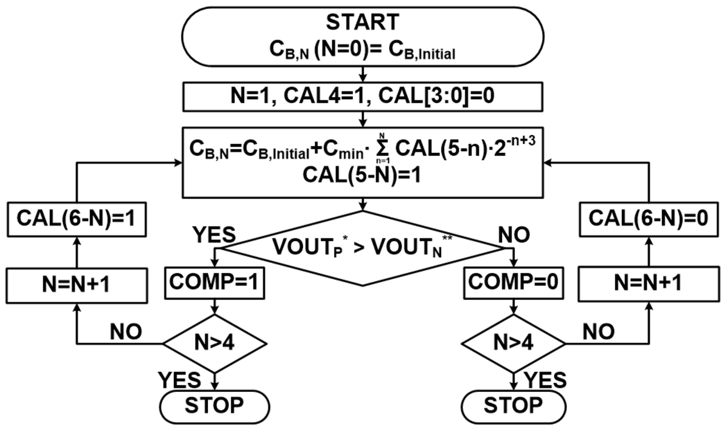
A flowchart of the calibration algorithm is shown in Figure 3. The total LSB capacitance, , connected in parallel within the C-DAC is given as,
where is the unit capacitor of theC-DAC. Moreover, the split capacitor before calibration is initialized to become . As the split capacitor becomes N-times calibrated, it becomes as,
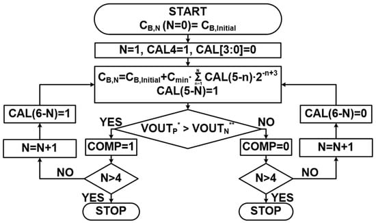
Figure 3.
Flowchart of the calibration algorithm based on the binary search technique. .
Since the total capacitance on the LSB node and split capacitor array of C-DAC can be obtained by a serial summation of and as ‘’, it can be expressed as,
where is a constant. The final goal of the calibration is to make ‘’ to be equal to unity [25].
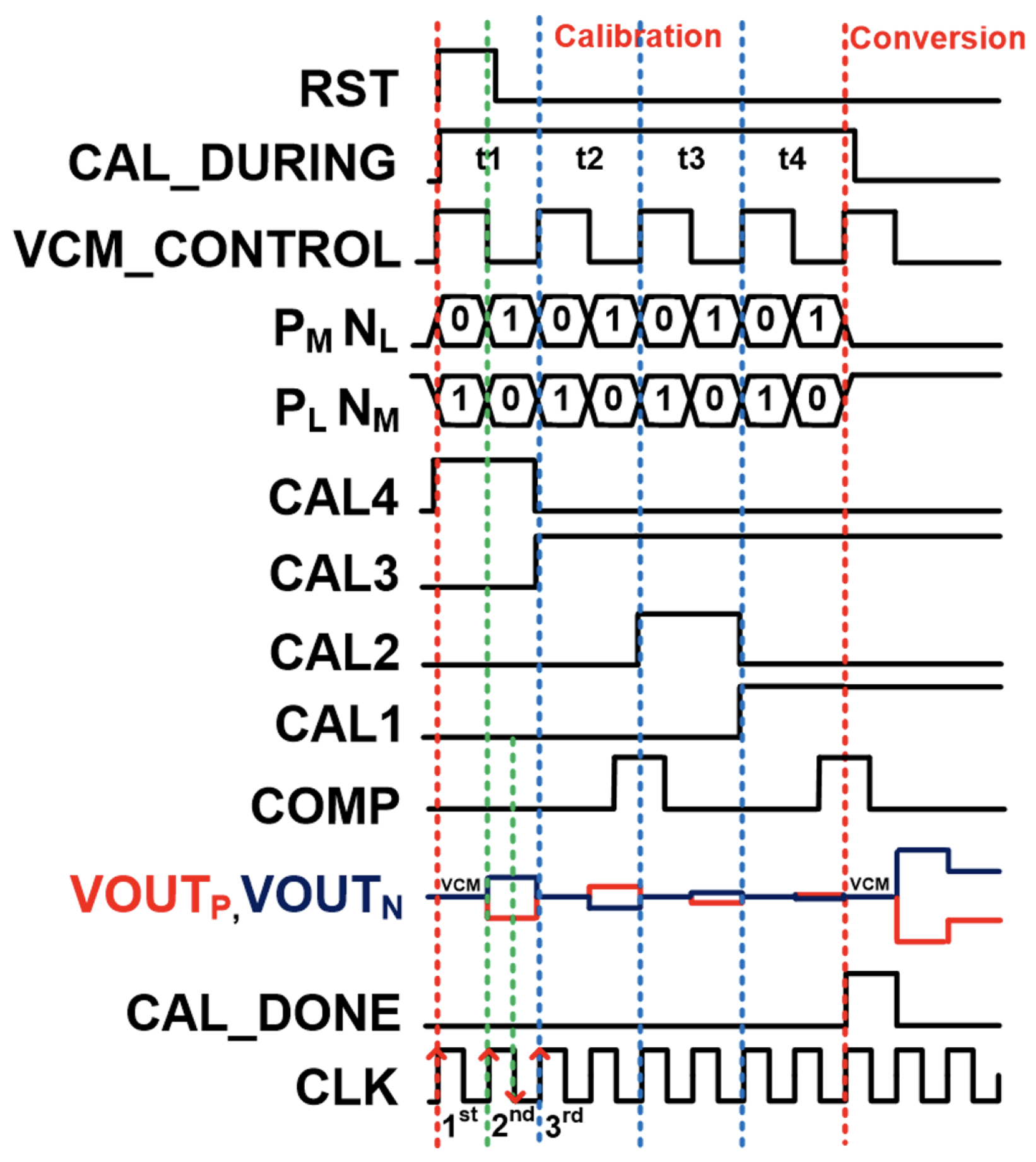
A timing diagram for the proposed binary search-based split capacitor calibration is shown in Figure 4. When the reset signal, RST, becomes high at the first clock, the internal signal of the calibration switch control logic, CAL_DURING, becomes high, and calibration proceeds.
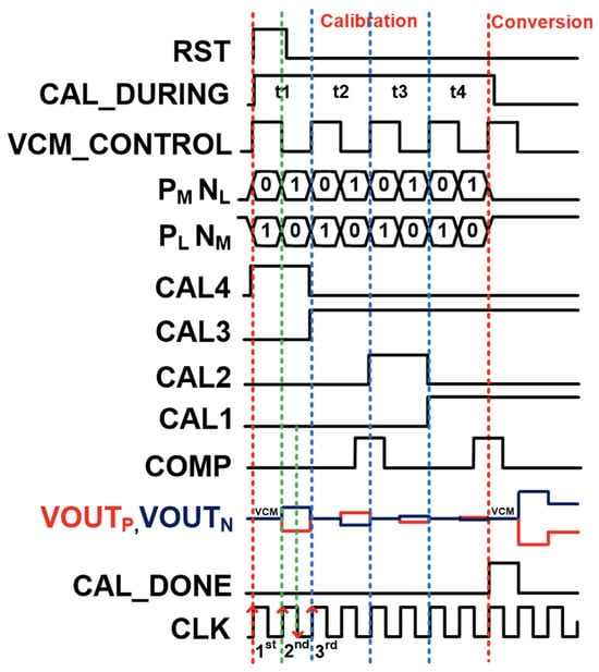
Figure 4.
Timing diagram of calibration logic.
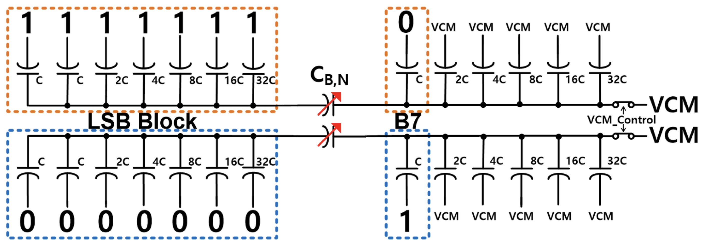
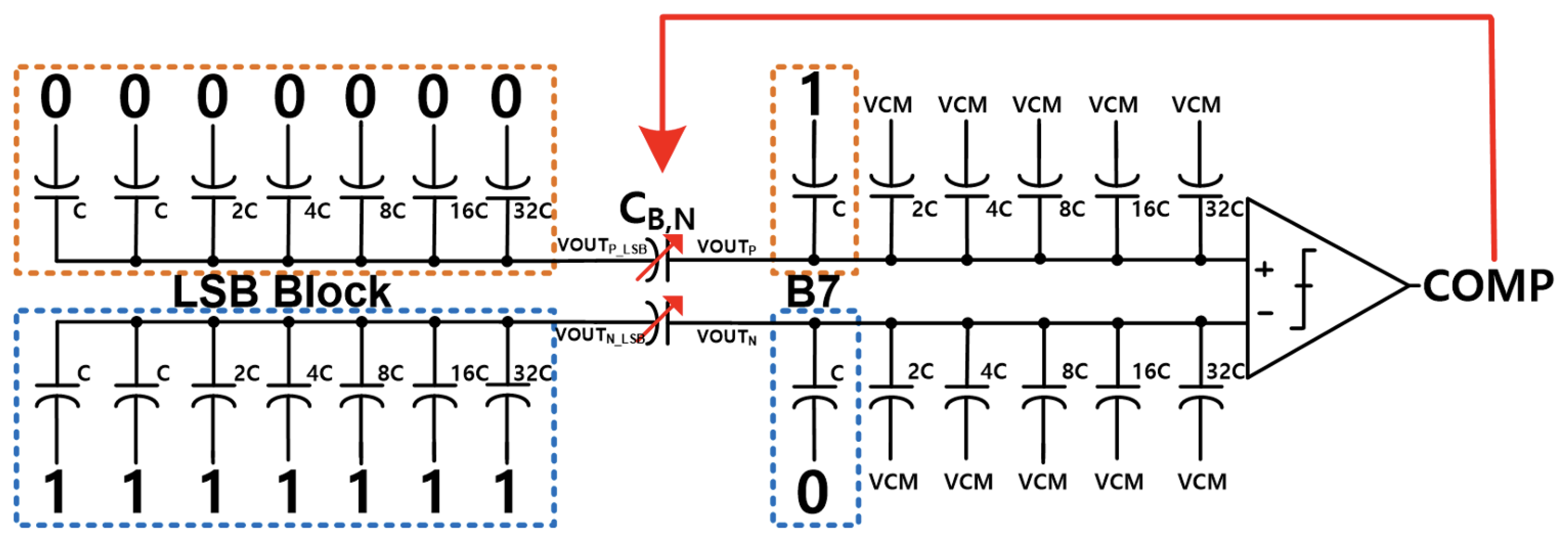
The first-phase calibration presented in Figure 5 is performed through two clocks. As the 1st CLK is on the rising edge, the common-mode control signal, VCM CONTROL, becomes high, so that VOUT and are connected to VCM, where VCM is the common mode voltage. As CAL4 is set to ‘1’ (CAL4 = 1), as shown in red box of Figure 6, the switch of the split capacitor array associated with turns on. In addition, [3:1] becomes low, and signals become low, and and signals become high. Hence, and signal the control capacitor of the LSB block, while and signal the control capacitor of each .
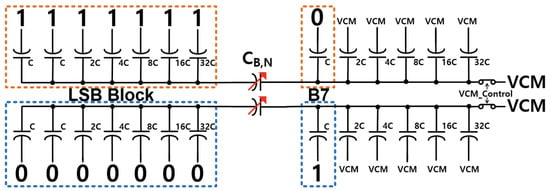
Figure 5.
C-DAC circuit during the 1st of the first-phase calibration.
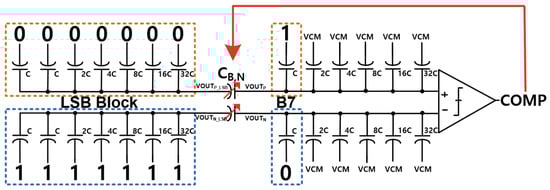
Figure 6.
C-DAC circuit during the 2nd CLK of the first-phase calibration.
The charges in the -DAC at the and nodes, and , are determined by,
As the 2nd CLK is on the rising edge, VCM_CONTROL signal becomes low, as illustrated in Figure 7. Therefore and are floated, and , and signal become toggled.
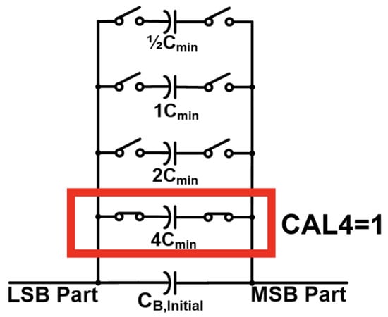
Figure 7.
Split capacitor array in the first-phase calibration with CAL4 = 1.
In the 2nd CLK falling edge, and signals are compared to determine the output signal of the comparator, COMP, so that the mismatch in split capacitors can be detected. In the timing diagram given, VOUT is less than VOUT, and the COMP signal becomes low. Reflecting the COMP signal, CAL4 becomes low at the 3rd CLK.
According to charge conservation, and are described as,
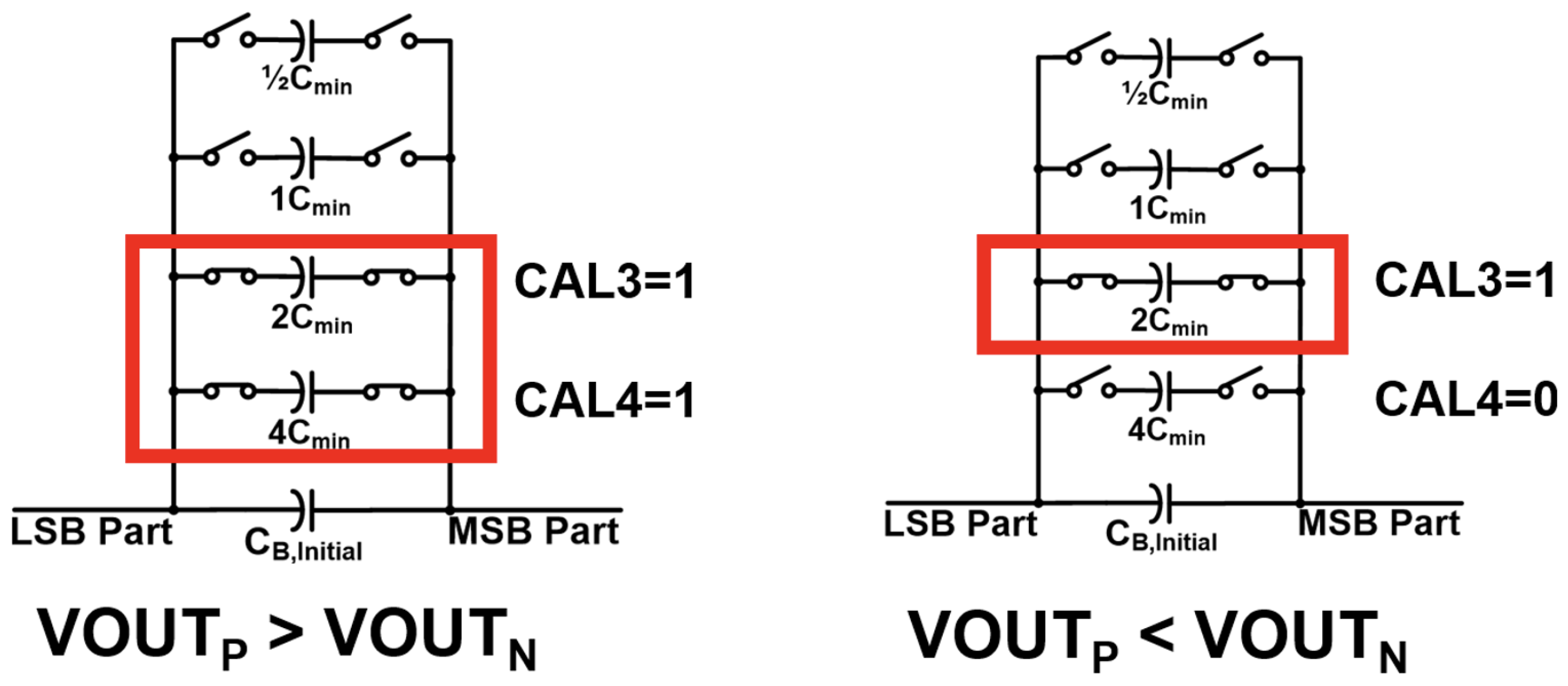
As VCM_CONTROL signal becomes high, it is set back to VCM during the 3rd CLK. CAL4 and CAL3 become low and high, respectively, to reflect the value of COMP during the previous 2nd in the timing diagram. Split capacitor that is half the weight of the split capacitor in the previous step is added.
If becomes larger than during the 2nd , then COMP , and CAL4 and CAL3 stay high, as presented in Figure 8. Otherwise, CAL4 stays low and CAL3 becomes high.
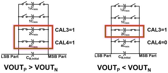
Figure 8.
Two possible statuses of split capacitor array , depending on and .
This calibration process is repeated four times ( and 8-CLK). VOUT and become closer to the VCM, so that becomes closer to . As the calibration is finished, CAL_DURING signal goes low, CAL_DONE signal becomes high, and signals become low, and and signals become high. Further, the foreground calibration is followed by the 12-bit data conversion.
Table 1 illustrates one example of operation of the binary search calibration algorithm in terms of CAL[4:1] and during the calibration times (t1∼t4), where is the calibration capacitor . As CAL[4:1] becomes ‘1000’ with the COMP signal as ‘0’ during t1, becomes . Since the COMP signal becomes low, CAL4 becomes ‘0’ to reflect the previous COMP signal, CAL3 becomes ‘1’, and changes from to during t2. Since the COMP signal stays high during t2, CAL3 remains ‘1’ and CAL2 sets to ‘1’, resulting in of during t3. Since the COMP signal moves from low to high during t3 to t4, CAL2 changes from ‘1’ to ‘0’ and CAL1 sets to ‘1’, so that becomes . Final CAL[4:1] and become ‘0101’ and , respectively.

Table 1.
The operational table of the binary search calibration algorithm in terms of CAL[4:1], COMP, , and calibration times (t1∼t4).
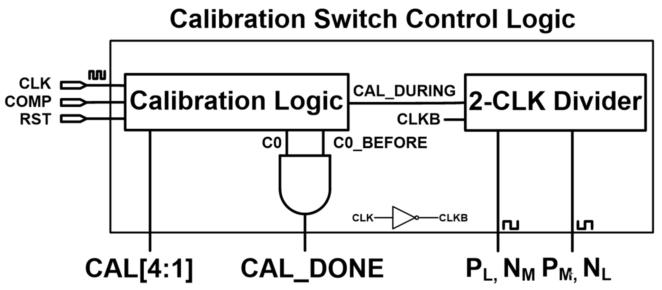
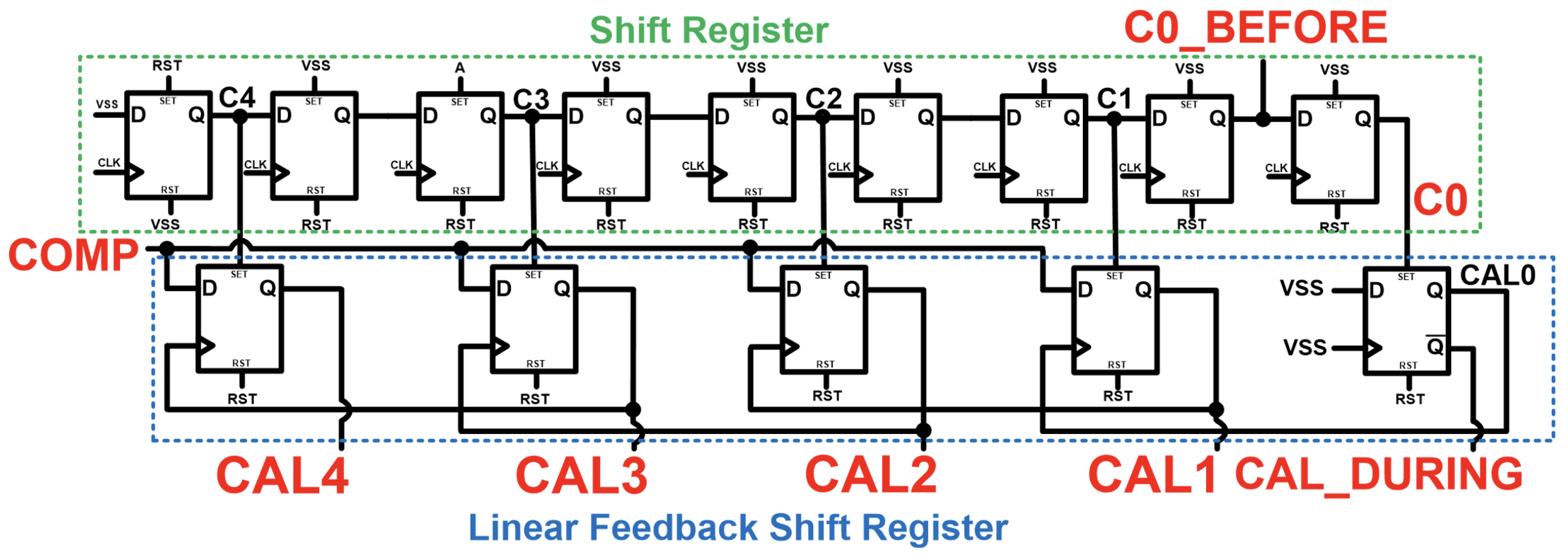
The block diagram of the calibration switch control logic circuit presented in Figure 9 contains the calibration logic and a 2-CLK divider. The circuit diagram of the calibration logic consists of an 8-bit shift register and a 4-bit LFSR (Linear Feedback Shift Register), as illustrated in Figure 10.
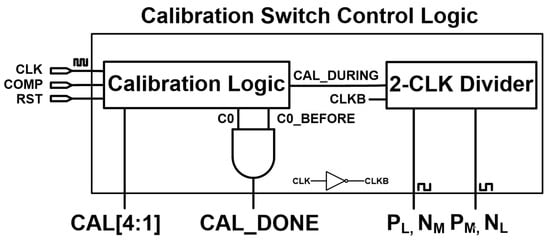
Figure 9.
Block diagram of calibration switch control logic.
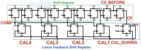
Figure 10.
Circuit diagram of the calibration logic.
The CAL_DONE signal is generated by the AND gate output of C0_BEFORE and from the calibration logic. As the CAL_DONE signal stays low and the CAL_DURING signal becomes high at the same time, the calibration process takes place. During the foreground calibration process, CAL[4:1] signals are determined to reflect the output of the comparator. These 4-bit calibration signals are used to control the split capacitor array.
The 2-CLK divider, as presented in Figure 11a, is implemented utilizing one JK flip-flop. It divides the CLK signal to generate signals. The CAL_DURING signal from the calibration Logic becomes input of the JK flip-flop within the 2-CLK divider.
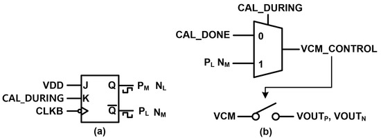
Figure 11.
Circuit diagram of (a) 2-CLK divider and (b) multiplexer to control the switch with and VOUT signals.
The multiplexer to control the switch with VCM_CONTROL signal is shown in Figure 11b. The CAL_DONE signal and the signals become the input signals of the multiplexer to generate the VCM_CONTROL signal with the CAL_DURING signal.
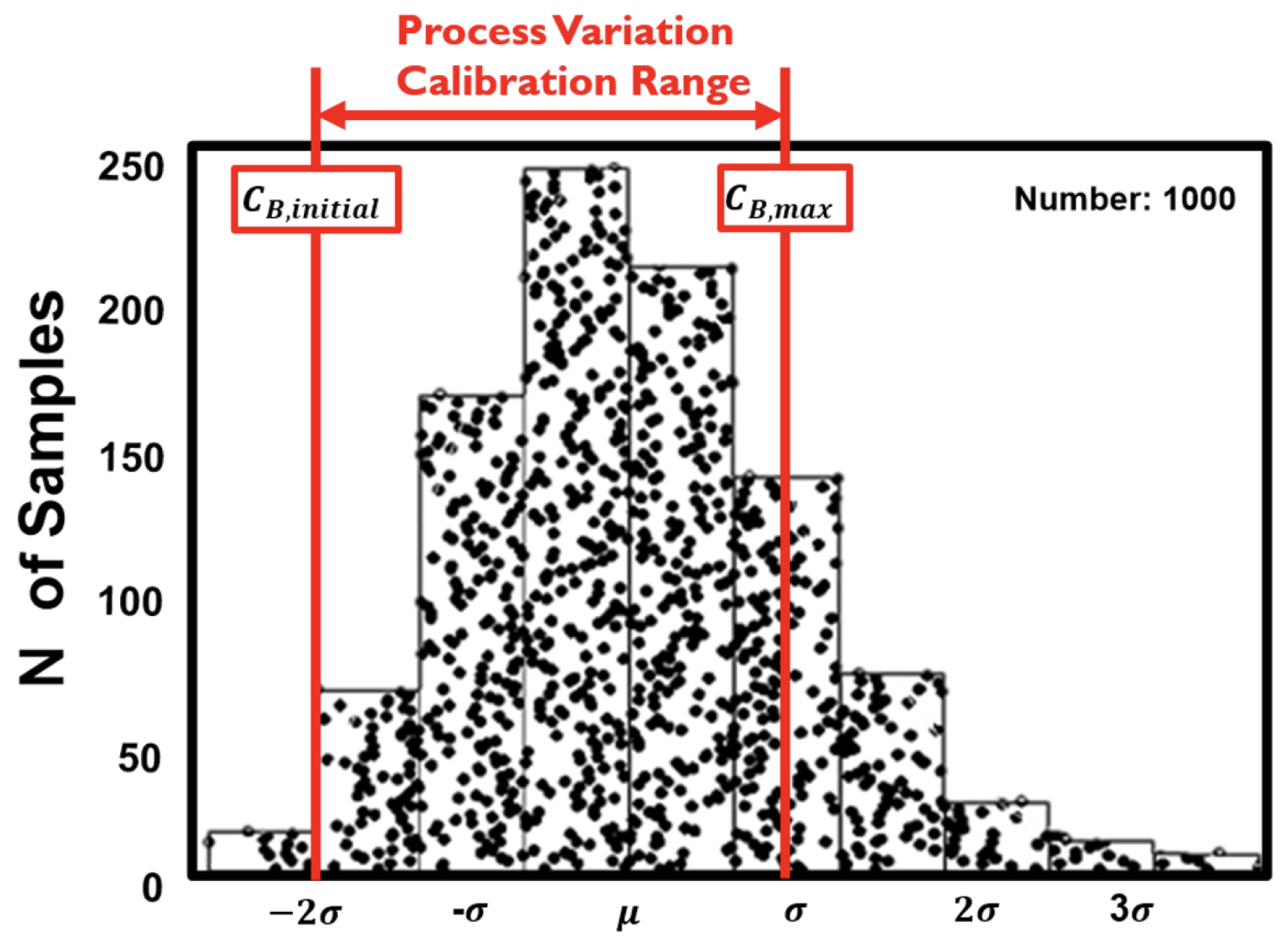
The proposed binary search calibration is influenced by process variation, as given by (10), where is the standard deviation of the process variation. is designed to be smaller than the ideal split capacitor. According to the binary search algorithm, can be increased up to , as given by (11).
The Monte Carlo simulation of the theoretical split capacitor in the process is illustrated in Figure 12. As the initial and maximum values of the variable split capacitor given by (10) and (11) are projected onto the graph, the process compensation range can be obtained approximately by to .
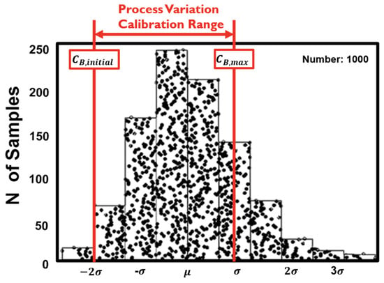
Figure 12.
Plot of process variation calibration range of the split capacitor .
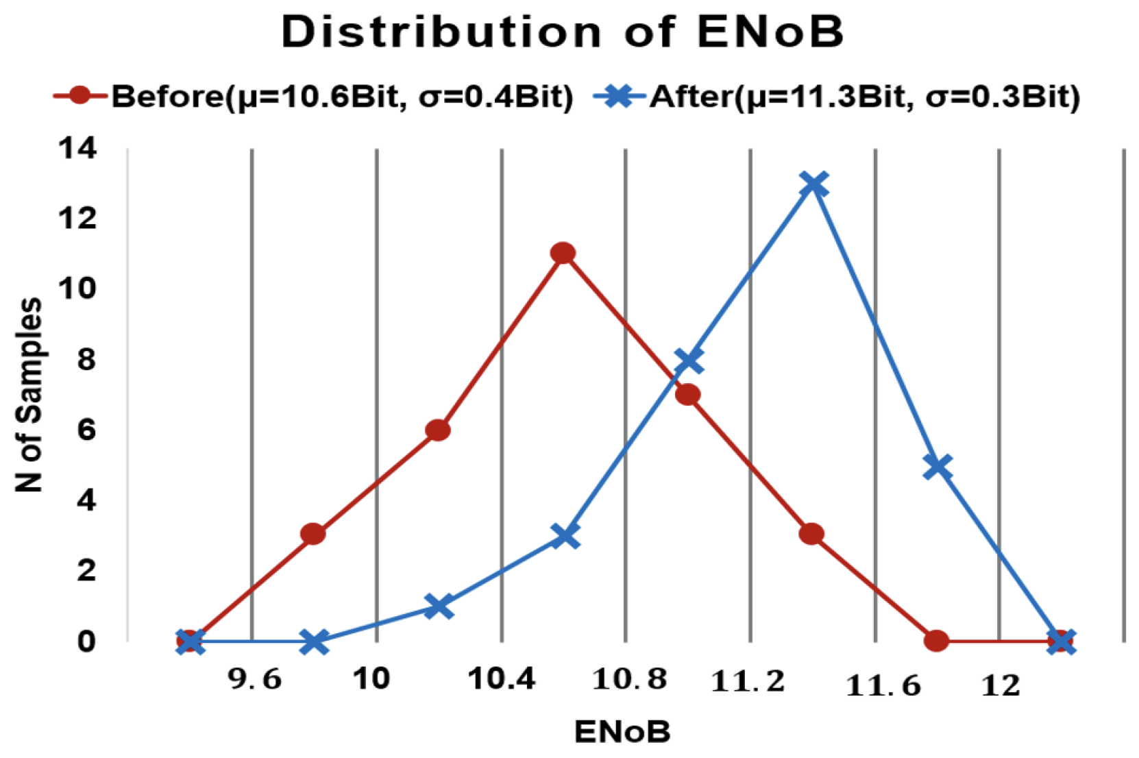
The plots of the ENoB distribution from Monte Carlo simulation for the before and after calibration conditions are compared in Figure 13. The mean value of ENoB before calibration becomes 10.6-bit and the mean value of ENoB after calibration becomes 11.3-bit. The distributions of the ENoB before and after the calibration are relatively left-leaning and right-leaning, respectively. It is confirmed that the performance of ENoB is improved through the proposed binary search calibration algorithm.
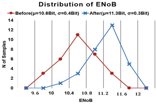
Figure 13.
Plot of ENoB distribution curve for before and after calibration in the Monte Carlo simulation.
3. Results
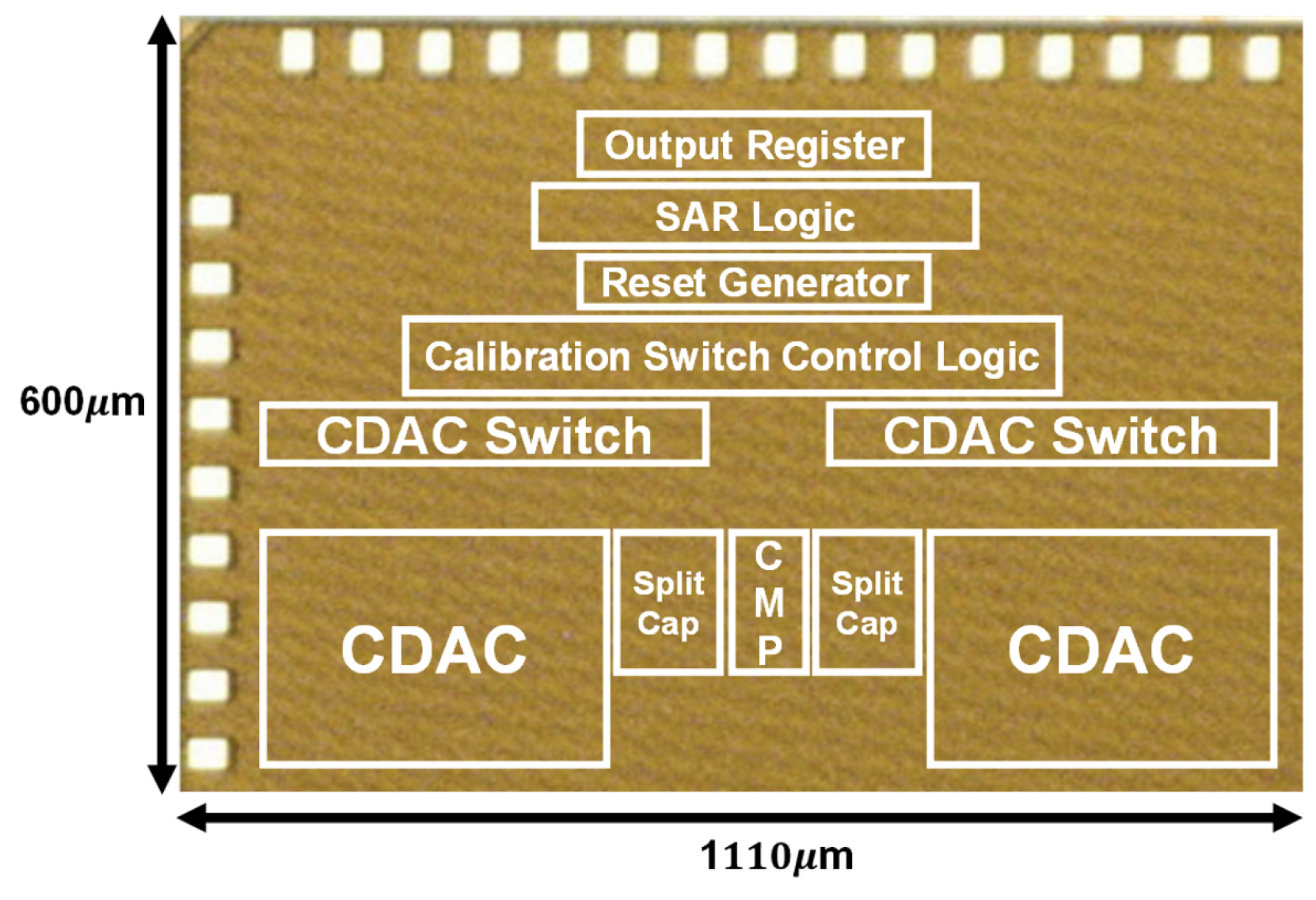
The proposed SAR ADC is implemented by a 28 nm 1-poly 8-metal CMOS (Complementary Metal Oxide Semiconductor) process. The chip photograph of the proposed SAR ADC with an area of is shown in Figure 14. The effective layout excluding bonding pads occupies . The 12-bit C-DAC, split capacitor array, and analog blocks of the comparator are located in the lower part of the layout. The digital blocks, including the C-DAC switches, calibration switch control logic, reset generator, SAR logic, and output register, are placed in the upper part. The design of the chip ensures physical and electrical separation between the analog and digital blocks of the chip.

Figure 14.
Chip photograph of the proposed SAR ADC.
A photograph of the PCB (Print Circuit Board) with the proposed ADC is presented in Figure 15. The PCB includes three SMA connectors for the differential input signals (VINP and VINN) and the clock signal (CLK), and five connectors (analog power nodes (AVDD (Analog Power Supply Voltage) and AVSS (Analog Ground)), digital power nodes (DVDD (Digital Power Supply Voltage) and DVSS (Digital Ground)), and VCM (common-mode node)). Three test pins to monitor three signals, namely RST, CAL_DONE, and , are placed adjacent to the proposed ADC chip for signal integrity purposes. The 12-bit digital output pins are placed on the upper portion of the PCB.
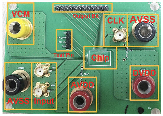
Figure 15.
Photograph of the proposed ADC Chip on PCB.
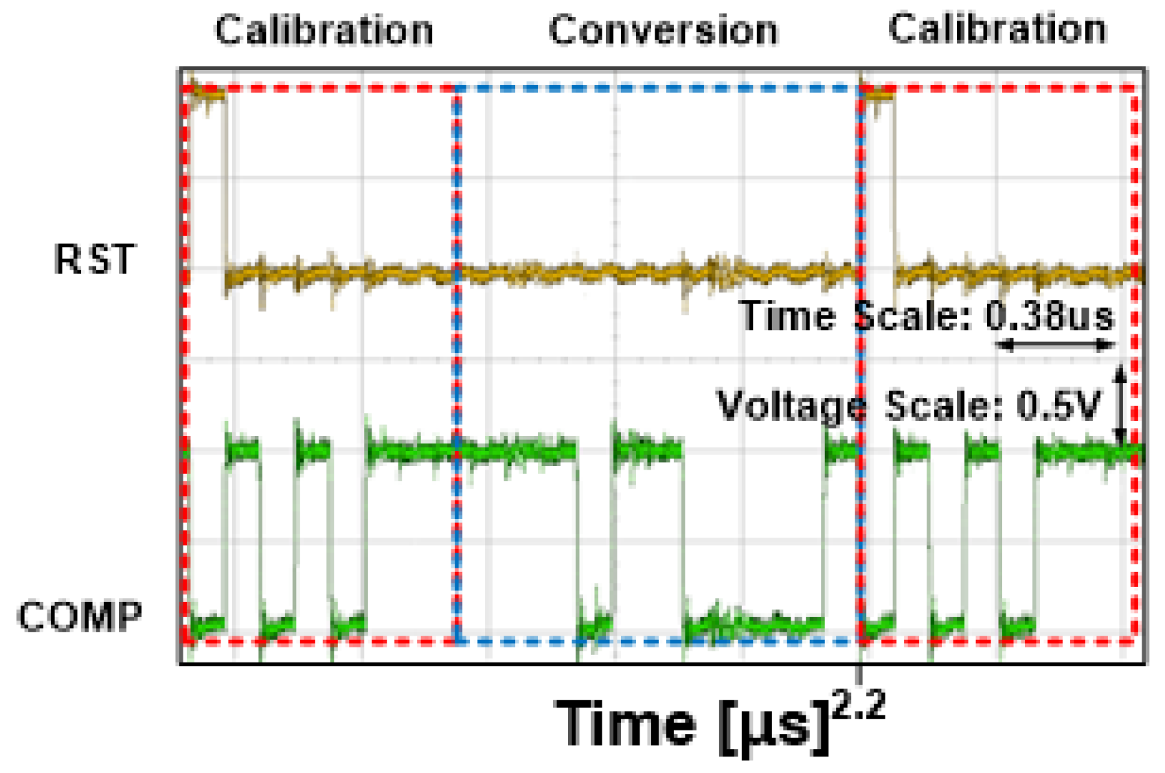
The measured waveforms of the CLK, RST, CAL_DONE, and signals are illustrated in Figure 16. As the RST signal becomes high, the binary search calibration algorithm performs for , the CAL_DONE signal becomes high at the end of the 8th , and the 12-bit data conversion operation is performed for 14 CLKs. During the calibration process, the frequency of the signal is reduced to half with respect to that of the clock signal during calibration time and becomes high during the conversion time. Figure 17 presents the measured waveform of the RST and COMP signals. As the COMP signal stays high during the calibration time (), the CAL[4:1] signal becomes ‘1111’ and becomes . These measurement results prove the proper functionality of the binary search calibration algorithm described in Table 1.
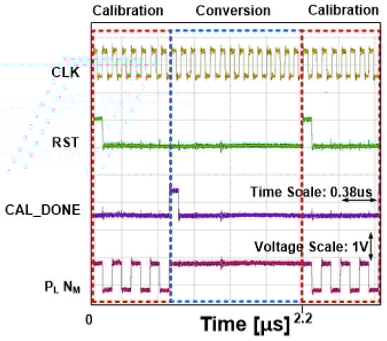
Figure 16.
Measured waveforms of the CLK, RST, CAL_DONE, and signals.
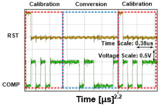
Figure 17.
Measured waveforms of the RST and COMP signals.
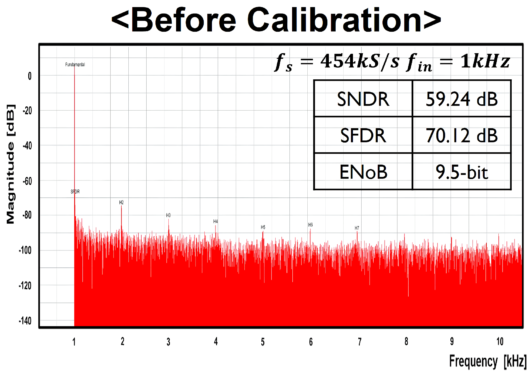
The INL and DNL before calibration shown in Figure 18 are measured to be and , respectively. On the other hand, the INL and DNL after calibration shown in Figure 19 are measured to be −1.8/1.7 LSB and LSB, respectively. Hence, the binary search calibration algorithm enhances the performance of the linearity of the proposed ADC by approximately 1 bit. The measured SNDR (Signal-to-Noise Distortion Ratio) and ENoB before calibration from FFT (Fast Fourier Transform) shown in Figure 20 are and 9.5-bit, respectively. After calibration, SNDR and ENoB are measured to be and 10.3-bit, respectively, as presented in Figure 21. The analog and digital power consumption are measured to be 16.1 and , respectively, resulting in a total power dissipation of 30.7 .
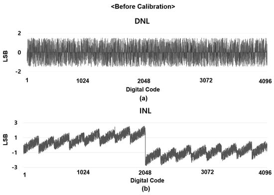
Figure 18.
Plot of linearity before calibration of (a) DNL and (b) INL.
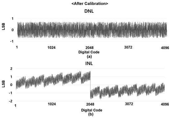
Figure 19.
Plot of linearity after calibration of (a) DNL and (b) INL.
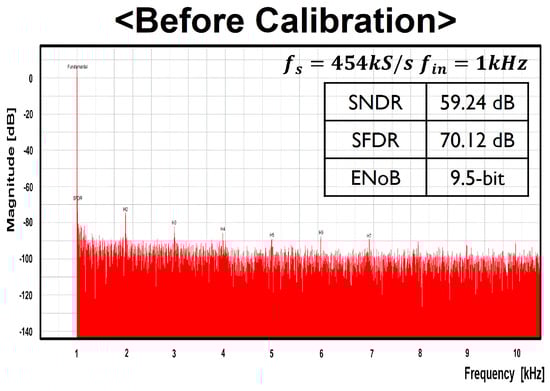
Figure 20.
FFT measurement result before calibration.
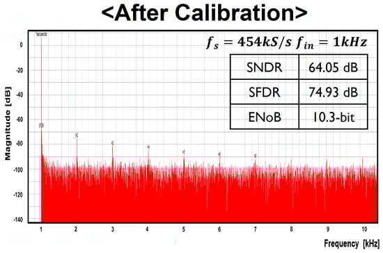
Figure 21.
FFT measurement result after calibration.
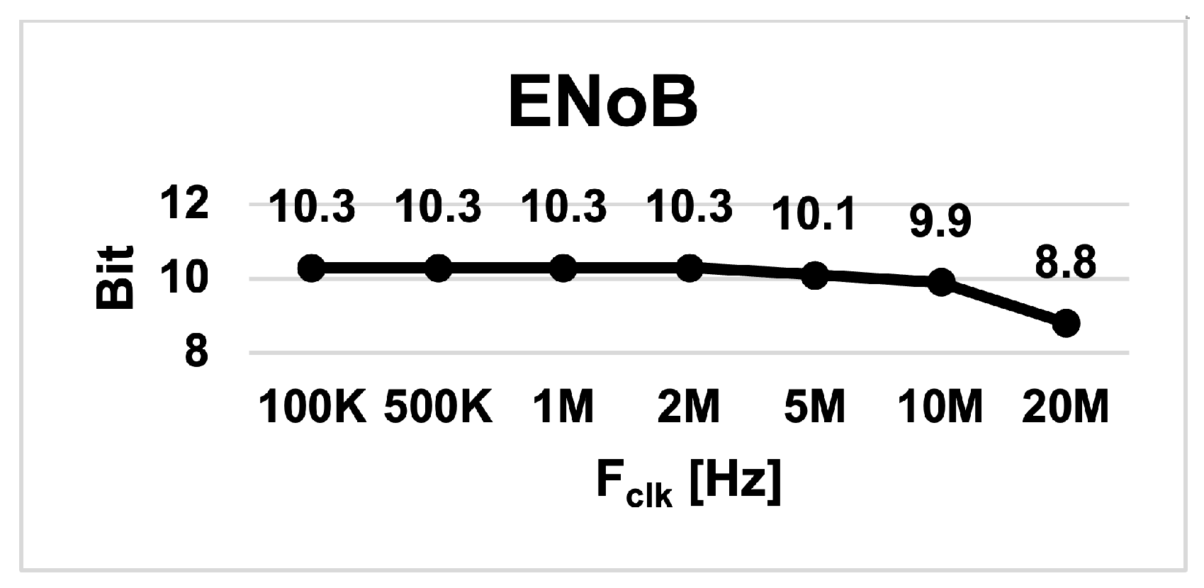
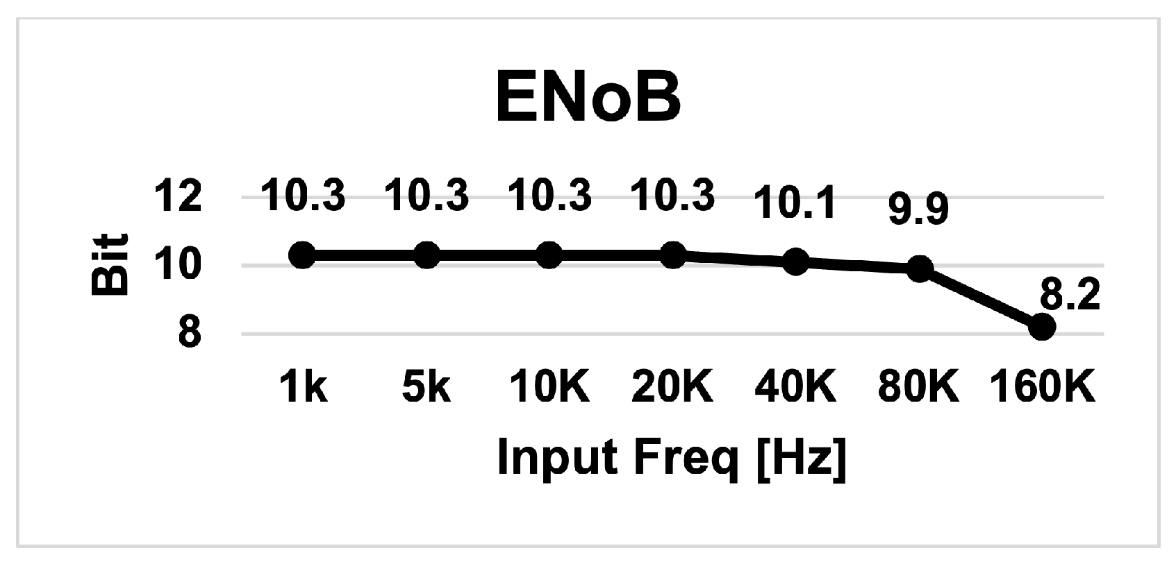
As the clock frequency varies from to with the input frequency fixed to , as shown in Figure 22, the measured ENoB remains at 10.3-bit up to and degrades to 8.8-bit afterwards. Figure 23 illustrates that the measured ENoB remains at 10.3-bit up to of the input frequency and decreases to 8.2-bit with the clock frequency fixed to .
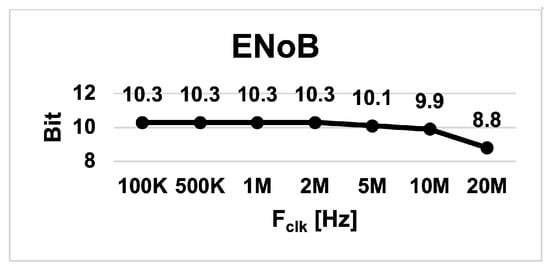
Figure 22.
Plot of ENoB as a function of clock frequency .

Figure 23.
Plot of ENoB as a function of input frequency .
A comparison of the static/dynamic performance parameters of the ADC between the proposed work and the conventional ones is made in Table 2. The authors of [8,12] employed the linear search algorithm and showed a comparable enhancement of INL/DNL and ENoB compared with the proposed work with the binary search algorithm. However, the proposed ADC with faster sampling rate performed with a lower power consumption and FoM. The works of [7,9,10,11] with the resolution of 12-bit and a SAR architecture the same as the proposed one exhibited comparative static/dynamic performances to the proposed one, except for calibration circuitry.
Table 2.
Performance comparison of the proposed ADC.
4. Conclusions
This paper proposes a 12-bit SAR ADC with foreground calibration using the binary search algorithm for biomedical signal processing. By incorporating calibration switch control logic into the conventional SAR ADC, the capacitance of the calibration split capacitor is determined within 8 clock signals by the binary search algorithm. The proposed binary search calibration algorithm with 4-bit resolution (CAL[4:1]) and a of is approximately 3.75 times faster than the conventional linear search calibration one. The proposed binary search calibration algorithm aims to ensure that the calibrated split capacitance closely matches the desired value, thus achieving optimal performance in the SAR ADC. Since a differential mode is employed in the C-DAC circuit, the linearity and ENoB performance of the proposed ADC are superior to those of the conventional single-ended mode. The proposed SAR ADC is implemented by a CMOS 1-poly 8-metal process with a supply voltage of . The effective layout area excluding bonding pads is . Measurement results of the proposed ADC after calibration show a power consumption of (analog and digital power of 16.1 and , respectively), INL of , DNL of −0.7/0.7 LSB, ENoB of 10.3-bit, and FoM of 53.7 step. The proposed 12-bit ADC with the binary search algorithm is applicable to low-power bio-signal processing and IoT platforms.
Author Contributions
Conceptualization, J.-I.Y. and K.S.Y.; methodology, J.-I.Y. and K.S.Y.; software, J.-I.Y.; validation, J.-I.Y. and K.S.Y.; formal analysis, J.-I.Y.; investigation, J.-I.Y.; resources, J.-I.Y.; data curation, J.-I.Y.; writing—original draft preparation, J.-I.Y.; writing—review and editing, H.L.; visualization, J.-I.Y.; supervision, K.S.Y. and H.L; project administration, K.S.Y.; funding acquisition, K.S.Y. and H.L. All authors have read and agreed to the published version of the manuscript.
Funding
This work was supported in part by a National Research Foundation of Korea (NRF) grant funded by the Korean government (MSIT) (2022R1F1A1069055), in part by the MSIT (Ministry of Science and ICT), Korea, under the Innovative Human Resource Development for Local Intellectualization support program (IITP-2023-RS-2023-00259678) supervised by the IITP (Institute for Information and Communications Technology Planning and Evaluation), in part by an Institute of Information and Communications Technology Planning and Evaluation (IITP) grant funded by the Korean government (MSIT) (No.RS-2022-00155915, Artificial Intelligence Convergence Innovation Human Resources Development (Inha University)), and in part by an Inha University Research Grant. MPW and Cadence design tools were supported by IDEC.
Institutional Review Board Statement
Not applicable.
Informed Consent Statement
Not applicable.
Data Availability Statement
The data present in this study are available on request from the corresponding author.
Conflicts of Interest
The authors declare no conflicts of interest. The funders had no role in the design of the study; in the collection, analyses, or interpretation of data; in the writing of the manuscript; or in the decision to publish the results.
Abbreviations
The following abbreviations are used in this manuscript:
| SAR | Successive Approximation Register |
| ADC | Analog to Digital Converter |
| CMOS | Complementary Metal Oxide Semiconductor |
| INL | Integral Non-Linearity |
| DNL | Differential Non-Linearity |
| LSB | Least Significant Bit |
| ENoB | Effective Number of Bits |
| FFT | Fast Fourier Transform |
| FoM | Figure of Merit |
| EEG | Electroencephalography |
| ECG | Electrocardiography |
| EMG | Electromyography |
| TS SS | Two-Step Single-Slope |
| R-DAC | Resistor Digital to Analog Converter |
| C-DAC | Capacitor Digital to Analog Converter |
| RFID | Radio-Frequency Identification |
| CLK | Clock Signal |
| RST | Reset Signal |
| CAL | Calibration Signal |
| COMP | Comparator Signal |
| PCB | Printed Circuit Board |
| AVDD | Analog Power Supply Voltage |
| AVSS | Analog Ground |
| DVDD | Digital Power Supply Voltage |
| DVSS | Digital Ground |
| VCM | Common-Mode Voltage |
| SNDR | Signal-to-Noise Distortion Ratio |
References
- Somappa, L.; Baghini, M.S. Continuous-Time Hybrid ΔΣ Modulators for Sub-μW Power Multichannel Biomedical Applications. IEEE Trans. Large Scale Integr. (VLSI) Syst. 2022, 30, 406–417. [Google Scholar] [CrossRef]
- Zhou, X.; Gui, X.; Gusev, M.; Ackovska, N.; Zhang, Y.; Geng, L. A 12-Bit 20-kS/s 640-nW SAR ADC with a VCDL-based Open-loop Time-Domain Comparator. IEEE Trans. Circuits Syst. II Express Briefs 2021, 69, 359–363. [Google Scholar] [CrossRef]
- Vafaei, M.; Hosseini, M.; Abiri, E.; Salehi, M. A 0.2-V 1.2 nW 1-KS/s SAR ADC with a Novel comparator structure for biomedical applications. Integration 2023, 88, 362–370. [Google Scholar] [CrossRef]
- Mao, W.; Li, Y.; Heng, C.H.; Lian, Y. A Low Power 12-Bit 1-kS/s SAR ADC for Biomedical Signal Processing. IEEE Trans. Circuits Syst. I Regul. Pap. 2018, 66, 477–488. [Google Scholar] [CrossRef]
- Zhang, Z.; Yu, Q.; Li, J.; Wang, X.Z.; Ning, N. A 12-Bit Dynamic Tracking Algorithm-Based SAR ADC with Real-Time QRS Detection. IEEE Trans. Circuits Syst. I Regul. Pap. 2020, 67, 2923–2933. [Google Scholar] [CrossRef]
- Lee, W.E.; Lin, T.H. A 0.6-V 12-Bit Set-and-Down SAR ADC with a DAC-Based Bypass Window Switching Method. IEEE Trans. Circuits Syst. II Express Briefs 2023, 70, 3223–3227. [Google Scholar] [CrossRef]
- Song, Z.; Ma, Z.H.; Yao, Y.; Zou, R.f.; Hu, J.G. A ENOB 10.3 bit, 103 μW ON-CHIP CALIBRATION SAR ADC. J. Phys. Conf. Ser. 2023, 2524, 012019. [Google Scholar] [CrossRef]
- Zhang, Q.; Ning, N.; Zhang, Z.; Li, J.; Wu, K.; Yu, Q. A 12-Bit Two-Step Single-Slope ADC with a Constant Input-Common-Mode Level Resistor Ramp Generator. IEEE Trans. Large Scale Integr. (VLSI) Syst. 2022, 30, 644–655. [Google Scholar] [CrossRef]
- De Venuto, D.; Castro, D.T.; Ponomarev, Y.; Stikvoort, E. 0.8 μW 12-bit SAR ADC Sensors Interface for RFID Applications. Microelectron. J. 2010, 41, 746–751. [Google Scholar] [CrossRef]
- Ding, M.; Harpe, P.; Chen, G.; Busze, B.; Liu, Y.H.; Bachmann, C.; Philips, K.; van Roermund, A. A Hybrid Design Automation Tool for SAR ADCs in IoT. IEEE Trans. Large Scale Integr. (VLSI) Syst. 2018, 26, 2853–2862. [Google Scholar] [CrossRef]
- Yang, S.; Zhang, H.; Fu, W.; Yi, T.; Hong, Z. A Low Power 12-bit 200-kS/s SAR ADC with a Differential Time Domain Comparator. J. Semicond. 2011, 32, 035002. [Google Scholar] [CrossRef]
- Brenna, S.; Bonfanti, A.; Lacaita, A.L. A 70.7-dB SNDR 100-kS/s 14-b SAR ADC with Attenuation Capacitance Calibration in 0.35-μm CMOS. Analog Integr. Circuits Signal Process. 2016, 89, 357–371. [Google Scholar] [CrossRef]
- Chung, Y.H.; Zeng, Q.F.; Lin, Y.S. A 12-bit SAR ADC with a DAC-Configurable Window Switching Scheme. IEEE Trans. Circuits Syst. I Regul. Pap. 2020, 67, 358–368. [Google Scholar] [CrossRef]
- Zhang, D.; Alvandpour, A. A 12.5-ENOB 10-kS/s Redundant SAR ADC in 65-nm CMOS. IEEE Trans. Circuits Syst. II Express Briefs 2016, 63, 244–248. [Google Scholar] [CrossRef]
- Zhang, H.; Tan, Z.; Chu, C.; Chen, B.; Li, H.; Coln, M.; Nguyen, K. A 1-V 560-nW SAR ADC with 90-dB SNDR for IoT Sensing Applications. IEEE Trans. Circuits Syst. II Express Briefs 2019, 66, 1967–1971. [Google Scholar] [CrossRef]
- Joshi, A.; Shrimali, H.; Sharma, S.K. Digitally Assisted Secondary Switch-and-Compare Technique for a SAR ADC. IEEE Trans. Circuits Syst. II Express Briefs 2021, 68, 2317–2321. [Google Scholar] [CrossRef]
- Hsieh, S.E.; Kao, C.C.; Hsieh, C.C. A 0.5-V 12-bit SAR ADC Using Adaptive Time-Domain Comparator with Noise Optimization. IEEE J. Solid-State Circuits 2018, 53, 2763–2771. [Google Scholar] [CrossRef]
- Harpe, P.; Cantatore, E.; van Roermund, A. A 10b/12b 40 kS/s SAR ADC with Data-Driven Noise Reduction Achieving up to 10.1b ENOB at 2.2 fJ/Conversion-Step. IEEE J. Solid-State Circuits 2013, 48, 3011–3018. [Google Scholar] [CrossRef]
- Jo, Y.J.; Kim, J.E.; Baek, K.H.; Kim, T.T.H. A 0.007 mm2 0.6 V 6 MS/s Low-Power Double Rail-to-Rail SAR ADC in 65-nm CMOS. IEEE Trans. Circuits Syst. II Express Briefs 2021, 68, 3088–3092. [Google Scholar] [CrossRef]
- Hou, Y.; Qu, J.; Tian, Z.; Atef, M.; Yousef, K.; Lian, Y.; Wang, G. A 61-nW Level-Crossing ADC with Adaptive Sampling for Biomedical Applications. IEEE Trans. Circuits Syst. II Express Briefs 2019, 66, 56–60. [Google Scholar] [CrossRef]
- Wang, J.; Zhu, Z. A 0.6-V 9-bit 1-MS/s Charging Sharing SAR ADC with Judging-Window Switching Logic and Independent Reset Comparator for Power-Effective Applications. IEEE Trans. Circuits Syst. II Express Briefs 2020, 67, 1750–1754. [Google Scholar] [CrossRef]
- Jung, D.K.; Seong, K.; Han, J.S.; Shim, Y.; Baek, K.H. A 0.5 V 10 b 3 MS/s 2-Then-1b/Cycle SAR ADC with Digital-Based Time-Domain Reference and Dual-Mode Comparator. IEEE Trans. Circuits Syst. II Express Briefs 2022, 69, 909–913. [Google Scholar] [CrossRef]
- Song, J.; Jun, J.; Kim, C. A 0.5 V 10-bit 3 MS/s SAR ADC with Adaptive-Reset Switching Scheme and Near-Threshold Voltage-Optimized Design Technique. IEEE Trans. Circuits Syst. II Express Briefs 2020, 67, 1184–1188. [Google Scholar] [CrossRef]
- Yoshioka, K. VCO-Based Comparator: A Fully Adaptive Noise Scaling Comparator for High-Precision and Low-Power SAR ADCs. IEEE Trans. Large Scale Integr. (VLSI) Syst. 2021, 29, 2143–2152. [Google Scholar] [CrossRef]
- Chen, Y.; Zhu, X.; Tamura, H.; Kibune, M.; Tomita, Y.; Hamada, T.; Yoshioka, M.; Ishikawa, K.; Takayama, T.; Ogawa, J.; et al. Split Capacitor DAC Mismatch Calibration in Successive Approximation ADC. IEICE Trans. Electron. 2010, 93, 295–302. [Google Scholar] [CrossRef]


Disclaimer/Publisher’s Note: The statements, opinions and data contained in all publications are solely those of the individual author(s) and contributor(s) and not of MDPI and/or the editor(s). MDPI and/or the editor(s) disclaim responsibility for any injury to people or property resulting from any ideas, methods, instructions or products referred to in the content. |
© 2024 by the authors. Licensee MDPI, Basel, Switzerland. This article is an open access article distributed under the terms and conditions of the Creative Commons Attribution (CC BY) license (https://creativecommons.org/licenses/by/4.0/).