Abstract
With the outstanding growth of Internet of Things (IoT) devices, security and power efficiency of integrated circuits can no longer be overlooked. Current approved standards for cryptographic algorithms are not suitable for constrained environments. In this context, the National Institute of Standards and Technology (NIST) started a lightweight cryptography (LWC) competition to develop new algorithm standards that can be fit into small devices. In 2023, NIST has decided to standardize the Ascon family for LWC. This algorithm has been designed to be more resilient to side-channel and fault-based analysis. Nonetheless, hardware implementations of Ascon have been broken by multiple statistical fault analysis and power analysis. These attacks have underlined the necessity to develop adapted countermeasures to side-channel and perturbation-based attacks. However, existing countermeasures are power and area consuming. In this article, we propose a new countermeasure for the Ascon cipher that does not significantly increase the area and power consumption. Our architecture relies on the nonvolatile feature of the Magnetic Tunnel Junction (MTJ) that is the single element of the emerging Magnetic Random Access Memories (MRAM). The proposed circuit removes the bias exploited by statistical attacks. In addition, we have duplicated and complemented the permutation of Ascon to enhance the power analysis robustness of the circuit. Besides the security aspect, our circuit can save current manipulated data, ensuring energy saving from 11% to 32.5% in case of power failure. The area overhead, compared to an unprotected circuit, is .
1. Introduction
Over the last decade, the microelectronics domain has undergone a tremendous leap forward. The Internet of Things (IoT) has exponentially increased communications between objects, offering new prospects for a smart city and a smart home, or even automotive applications. The deployment and sustainability of these objects rely on small and low-power circuits [1]. Furthermore, sensitive information can be shared by IoT nodes, thus implying to strengthen the security of IoT objects.
Conventional cryptography algorithms, such as the Advanced Encryption Standard [2], were designed to be implemented on desktop or server environments, which render their use impracticable in constrained devices. To tackle this challenge, the cryptographic community actively researches alternative security primitives fulfilling the requirements of IoT circuits. Following this effort, several LWC algorithms have emerged. These algorithms are named after their low energy impact and area footprint. In 2017, the National Institute of Standards and Technology (NIST) initiated a process to evaluate and standardize LWC algorithms. All algorithms submitted in this process must implement an Authenticated Encryption with Associated Data functionality.
Recently, the NIST awarded the Ascon authenticated cipher [3] for lightweight cryptography standardization. It was already selected as the primary choice in the lightweight category in an earlier CAESAR competition [4]. During the standardization process, several power-analysis-based and statistical-fault-based attacks on Ascon [5,6,7] have emphasized the necessity to develop tailored countermeasures to secure the implementation of the cipher. These attacks either target the beginning or the end of the encryption process. To preserve the lightweight feature of Ascon, the countermeasure should keep its power and area consumption criteria.
To date, IoT objects are traditionally powered through physical connection or battery-based systems. However, it is not scalable and batteries have a limited lifetime. To ensure a better operability of IoT devices, energy harvesting techniques are currently under intensive research [8]. These techniques consist of harvesting energy from different external sources and convert it into electricity. Nonetheless, a continuous power delivery cannot be assured by these systems, as the energy of ambient sources may be intermittent or the energy harvested could be insufficient for the IoT objects to operate properly. Consequently, IoT devices relying on energy harvesting systems could be subject to data loss.
To reduce the power consumption of current hardware architectures, several nonvolatile memories have been proposed. Among these innovating technologies, the Spin Transfer Torque MRAM (STT-MRAM) [9] has lured digital designers to use them for designing low-power applications. A CMOS/MRAM hardware implementation of Ascon has already been put forward in the literature [10]. The authors have developed an ASIC design flow to implement hybrid CMOS/MRAM circuit using existing Electronic Design Automation (EDA) tools. They have substituted all volatile CMOS Flip-Flops with Nonvolatile Flip-Flops (NVFF) in the permutation, in the round counter, and in the Finite State Machine (FSM). This hybridized implementation enables the cryptographic primitive to quickly recover from an unplanned power failure. This architecture ensures energy savings ranging from 11% to 48% at the cost of a 5.5% area overhead compared to a CMOS reference implementation. Besides the low-power aspects, the nonvolatile feature could be used to store intermediate state before any potential fault injection attack. The faulty state could be substituted with the correct state saved in the memory to thwart the effect of fault injection.
2. Our Contribution
In this paper, we present a novel hardware countermeasure for the Ascon cipher, based on the association of CMOS and STT-MRAM.
This countermeasure relies on:
- A duplicated-complemented permutation for which the internal state S and its complemented value are computed in parallel.
- A Differential Novolatile Flip-Flops (DNVFF) adding the nonvolatility property to the internal state registers of the duplicated-complemented permutation. This DNVFF combines two CMOS FF and a nonvolatile circuitry.
The protection strategy is based on:
- Saving the states S and in the penultimate round of each encryption before potential attacks. Faults are detected by xoring the tag T with its inverted value . If a fault is detected, faulty states can be corrected, thus preventing an attacker from exploiting injected faults. To assess the effectiveness of the proposed countermeasure, we have performed Statistical Ineffective Fault Analysis (SIFA) [11] and Subset Fault Analysis (SSFA) [7] on both unprotected and protected version of the cipher.
- Reducing the dependency between manipulated data and power consumption thanks to the duplicated-complemented permutation, which makes it more difficult to recover the key by means of side-channel analysis. We have also conducted both a Correlation Power Analysis (CPA) and Differential Power Analysis (DPA) [5] on Ascon. These evaluations have been performed through power analysis simulations.
Note that the proposed circuit can also save current manipulated data, enabling consequent energy saving in case of power failure. To implement our countermeasure, we have targeted the CMOS 28 nm FD-SOI Design Kit (DK) from STMicroelectronics.
The remainder of this paper is structured as follows. Section 3 presents the Ascon cipher and introduces the STT-MRAM. Existing side-channel and fault-based analyses are also described. In Section 4, we explain the design and the operation of our proposed solution. Section 5 is devoted to the results of this study. The two last sections are dedicated to the discussion and conclusion.
3. Background and Related Work
This section opens with a brief description of Ascon. Then, we define STT-MRAM and its modes of operation. This background is closed by the presentation of the methodologies used for both side-channel and fault-based attacks. In the rest of this paper, denotes a bitwise XOR operation between a and b, and refers to a bitwise AND operation between a and b.
3.1. Description of Ascon
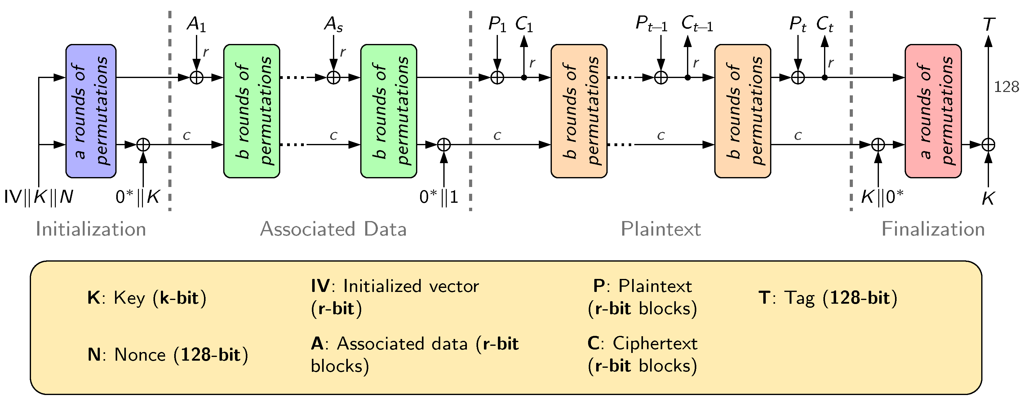
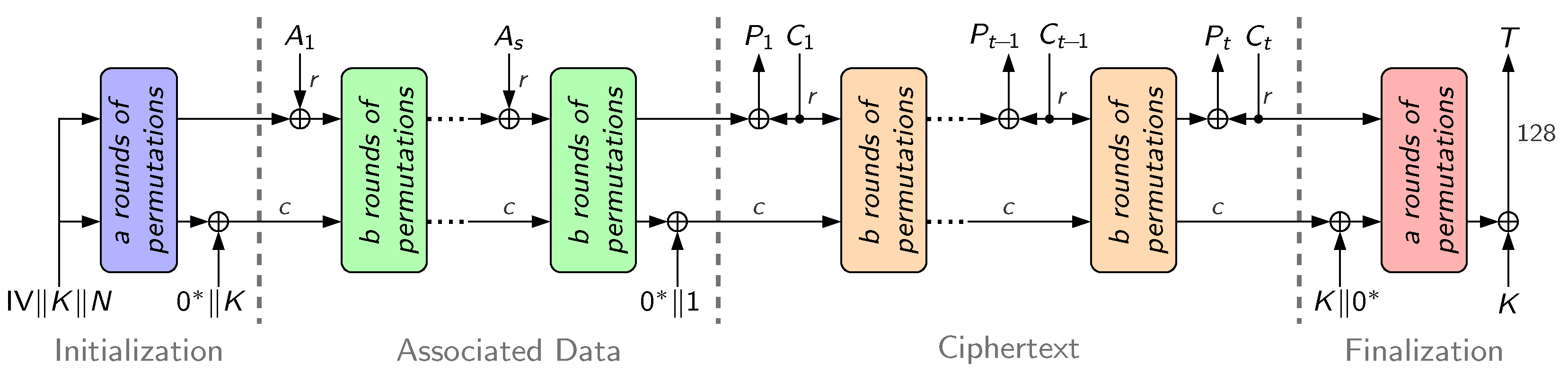
Ascon [3] is an Authenticated Encryption with Associated Data algorithm, which also offers some hashing functionalities. The encryption process is depicted on Figure 1. The algorithm operates on a 320-bit state S divided into a rate part and a capacity part , where . The block size of the data injected within the algorithm is defined by the rate part r.
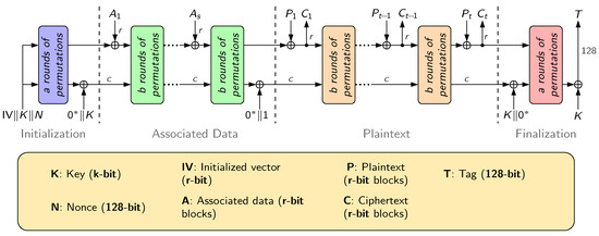
Figure 1.
Encryption mechanism of the Ascon cipher.
The encryption unfolds in four phases. In the beginning, the state takes a public nonce N, a private key K, and an initialization vector . The nonce prevents replay attacks when it is used in a stateful protocol. Associated data and plaintext are injected by a block of r bits in the second and the third phase, respectively. The associated data are used to bind a ciphertext to a context, so that it cannot be used for other purposes. The second phase is not processed if there are no associated data. The resulting blocks of ciphertext are extracted in the third phase. The authentication tag T is produced by xoring the algorithm end state with the key K. This tag ensures the integrity and the authenticity of the encryption.
Decryption also has four phases. Its process is shown in Figure 2. The main difference with the encryption scheme is the third phase, which decrypts each r-bit ciphertext block into r-bit plaintext. The other three phases remain unchanged.
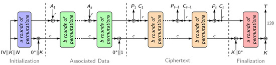
Figure 2.
Decryption mechanism of the Ascon cipher.
The permutation of Ascon consists of an iterative execution of either a or b round transformations. The internal state is split into five 64-bit words . Regarding the round transformation, it is composed of a constant addition to , a substitution layer, and a diffusion layer. The substitution layer is formed with a 5-bit nonlinear S-Box. Each S-Box depends on one bit of each word. The diffusion layer operates on each word separately.
In this article, only the encryption mechanism is targeted. We have conducted all our experiments on the Ascon-128 variant, meaning that a = 12, b = 6, r = 64, c = 256, and k = 128.
3.2. STT-MRAM
An STT-MRAM is a passive element composed of a Magnetic Tunnel Junction (MTJ), which is itself formed by two FerroMagnetic (FM) layers separated by an insulating tunnel barrier. A typical MTJ stack is illustrated on Figure 3.
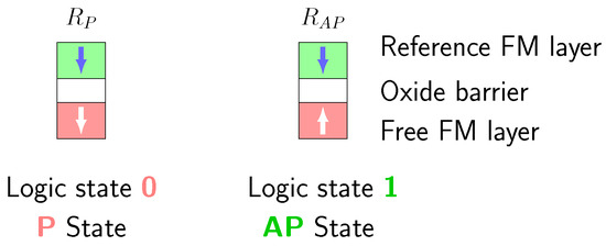
Figure 3.
MTJ with its different magnetization configurations.
The magnetization of the reference FM layer is always fixed, while the other FM layer can toggle between AntiParallel and Parallel state (AP and P, respectively). The read and write operations are achieved by allowing an electrical current to flow through it. The resistance in AP state is denoted whereas , which is lower than , refers to the resistance in the P state. Conventionally, represents logic 1 and logic 0. The resistance ratio between the two magnetic states is expressed as the Tunnel Magnetoresistance Ratio .
3.3. Statistical Ineffective Fault Analysis (SIFA)
SIFA uses the probability that the fault injected does not lead to a successful disruption of the device [12]. In other words, the injected fault affects the execution of the encryption in such a way that the final output is not influenced. SIFA assumes that the fault distribution exhibits a nonuniform characteristic under ineffective fault injection. The bias observed in the fault distribution can be exploited to distinguish the correct key hypothesis from the incorrect key hypothesis. The statistical distinguisher used by SIFA is the Squared Euclidean Imbalance (). It can be calculated as:
where refers to the fault probability distribution and represents a uniform distribution.
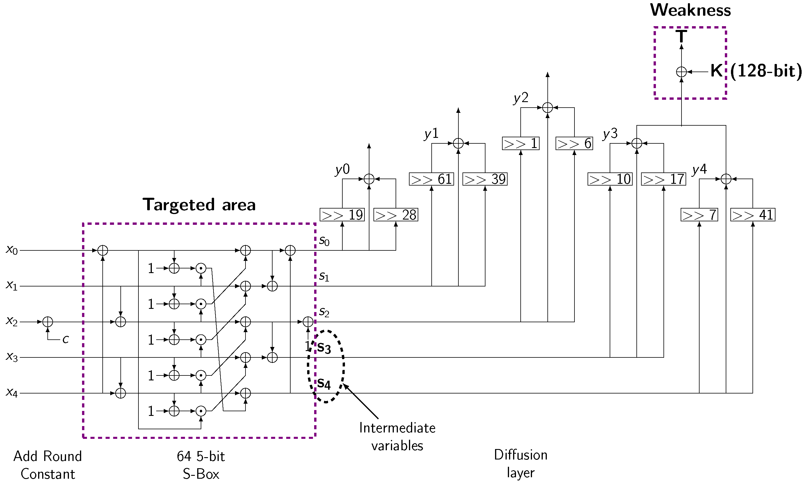
For the Ascon cipher, K. Ramezanpour et al. [11] have conducted SIFA on the last round of the finalization stage. The cryptanalysis is performed on the S-Box outputs before the tag T is released as represented in Figure 4. In this figure, is the input of the permutation, denotes the output of the substitution layer and is the output of the diffusion layer. The linear mapping of the inverse diffusion layer can be represented in matrix form as:
where is a sparse matrix of dimension . The first row of matrices has nonzero elements at locations which represent the right shift value of the diffusion function i. The second row is calculated by shifting the first row to the right by one element, and so on. Given a S-Box j, the output bits and can be expressed as:
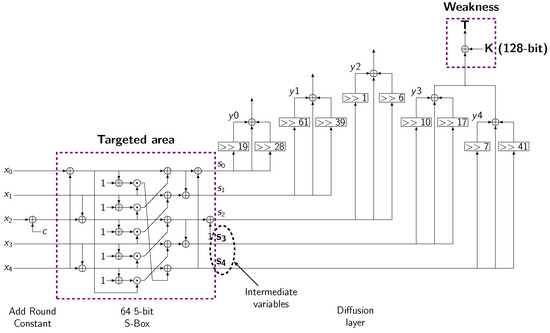
Figure 4.
Fault analysis on the last round of the Finalization phase.
In this relation represents the first and second parts of the tag, denotes the key bits, and is the r-th element in the j-th row of the inverse diffusion matrix .
As inverse diffusion matrices and contain, respectively, 33 and 35 nonzero elements [13], computing and using (3) and (4) would require to make assumptions on bits of the key. To reduce the key search hypothesis, ref. [11] proposed a double-fault methodology and a key dividing strategy.
Double-fault: The methodology consists of injecting faults into two S-Boxes . The statistical analysis is performed using the bits and . The intermediate variables can be referred as a 2-bit variable .
Key dividing strategy: The 128-bit key is divided into words of n bits, where n is a power of 2. Equations (3) and (4) can be rewritten using bits within the key word:
where:
The hypothesis for a S-Box j is expressed using the key bit combinations :
Hence, for every pair of S-Boxes, the corresponding key hypothesis is the vector . To retrieve the whole key, double-fault experiments are needed. Consider a case where n is set to 64. Therefore, 63 pairs of S-Boxes must be attacked and the key hypothesis contains four elements, meaning that there are sets of possible vectors .
The presented attack involves two steps which are described in two algorithms:
Algorithm 1: Find all possible values of using SIFA. Perform N encryptions targeting S-Box pairs . A set of correct tags is obtained. Intermediate variables are computed using (5) and (6). For every pair of S-Boxes, the number of correct key guesses is equal to .
Algorithm 2: Recover the key bits. Set to one of possible guesses from Algorithm 1. Among different guesses for , select one that has the same value of as in . Proceed the same way for others . At the end, we get a vector . This sequence is then used to retrieve key bits with (7). If the key found is incorrect, repeat the procedure by selecting another value of .
3.4. Subset Fault Analysis (SSFA)
As far the SSFA is concerned, it also exploits the bias introduced in the fault distribution [7]. Nonetheless, SSFA only considers effective faults. To the best of our knowledge, this attack was only proposed on Ascon. The targeted fault model is a bit-reset. When the input of the substitution layer is set to 0, the XOR operation between and is biased. SSFA reuses the same key dividing methodology introduced with the SIFA, but does not require a double-fault injection.
The attack combines two phases computed by two algorithms:
Algorithm 1: Find all possible values of using SSFA. Perform N encryptions targeting S-Box . We get a set of faulty tags. Intermediate variables are computed using (5) and (6). For every S-Box, the number of correct key guesses is equal to .
Algorithm 2: Recover the key bits. Select one of correct key guesses for each S-Box. We get a vector . This set is then used to find key bits with (7). For , there are solutions to test in the worst case.
3.5. Side-Channel Attacks
Side-channel attacks on Ascon rely on the well-known Differential Power Analysis (DPA) [14] and Correlation Power Analysis (CPA) [15]. The encryption process of Ascon start by initializing a constant vector , the key , and a public nonce (see Figure 1). From that point, only the key is unknown [5]. It can be recovered by performing several encryptions with different nonce. The output register after one round computation is defined by:
For a S-Box j, the output bit can be expressed in the Algebraic Normal Form:
From this relation, all bits that do not have an influence on power consumption can be removed:
where depends on one bit from key () and two bits from two parts of the nonce ( and ). If we combine (9) and (11):
Additions to index j are computed modulo-64 as the bits are located in a 64-bit register. To retrieve , the register can be targeted. In similar fashion, can be expressed as:
where . By varying the nonce for each encryption, all key bits can be retrieved. Equation (13) requires to find before .
3.6. Related Work
In the literature, several CMOS/MRAM implementations of lightweight ciphers have been investigated [10,16]. Such implementations embed NVFF to save intermediate state and algorithm progression. These implementations are compatible with the CMOS manufacturing process. They have been shown to be energy efficient, considering several use cases. Nevertheless, they have only covered the power aspect of hybrid architectures.
Regarding the existing countermeasures to SIFA, Saha et al. [17] used masking and repetition code techniques. Their solution has been reported to be successful in protecting against ineffective faults. However, the area overhead is not negligible (). In [18], the authors proposed a duplication method to protect PRESENT cipher [19]. In their implementation, the permutation and its duplicate version compute either the state or the inverted state. Their architecture can remove all biases exploited by SIFA. Compared to an unprotected version, the area overhead is about .
Among the many hardware implementation of Ascon algorithm, we choose to implement an unprotected version of Ascon-128 authenticated cipher with only one permutation round per clock cycle executed a = 12 or b = 6 times during the process and a 64-bit data block interface (r = 64). A 320-bit register saves the intermediate state of Ascon. Additional FSM and counter ensure the correctness of computation during all phases of the encryption process (see architecture in Figure 7).
In this work, we propose a CMOS/MRAM based countermeasure to protect against SIFA and SSFA. Our implementation also enhances the robustness against side-channel analysis. Moreover, our architecture is capable of saving intermediate states, thus enabling to restart the encryption from the last backup point after a power-off phase.
4. Proposed Solution
4.1. Core Idea
As a reminder, an effective fault occurs when the injected fault affects the execution of the process and changes the final output. If the injected fault does not change the final output, it is an ineffective fault. To protect the cipher against both SIFA and SSFA, it is necessary to detect both effective and ineffective faults. In other words, the bias in fault distribution must be removed whatever the fault model. To do so, we propose to correct all faults introduced in the last round of the encryption procedure. With SSFA, it would not be possible to steal the secret key since there is no faulty tag. With SIFA, an attacker could not discriminate correct tags from faulty tags.
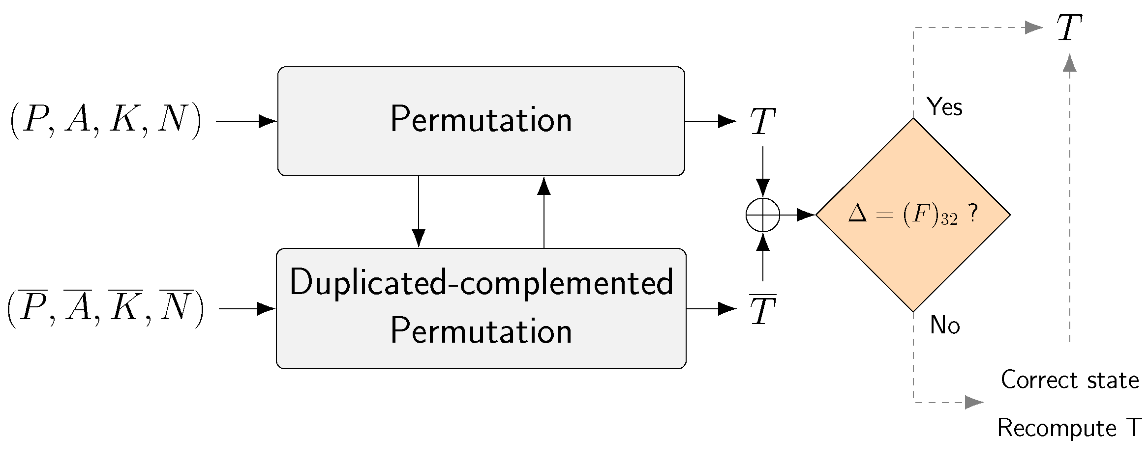
To detect injected faults, we designed a second instance of Ascon permutation in such a way that the Boolean equations and internal states are complemented. For example, the original is transformed into . This duplicated-complemented permutation allows us to compute . At the end of the Finalization stage, tag (T) is compared with its complemented value (). If no faults are introduced, no correction is necessary. If faults are detected, the state is corrected and T is recomputed. The architecture is illustrated in Figure 5.
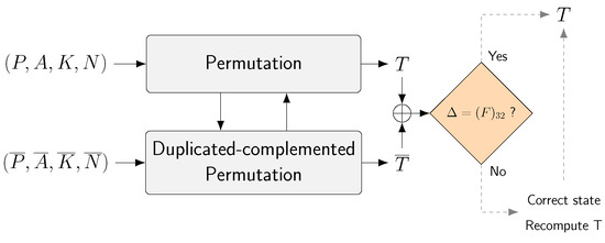
Figure 5.
Overview of the proposed countermeasure.
4.2. Differential Nonvolatile Flip-Flop Design
To correct faulty state, we save the content of intermediate state register at the penultimate round. To this end, all FFs in the state register were substituted by DNVFFs. This DNVFF is composed of two CMOS FFs, with a shared nonvolatile circuitry. It is represented in Figure 6. The basic operation is described below:
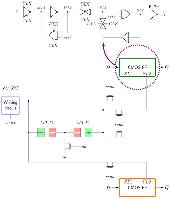
Figure 6.
Differential Nonvolatile Flip-Flop (DNVFF).
- CMOS FFs are based on transmission gate DFF triggered by a rising edge of the clock. When the asynchronous reset is asserted, the output is forced to 0.
- When the write signal is enabled, both and are stored into and . MTJs are always in opposite states. As the memory is nonvolatile, information is retained even if power is removed.
- When the read signal is enabled, nodes are discharged through pass transistors. Depending on MTJ resistance values, two nodes will be forced to 0 and two nodes will be forced to 1. The read operation can only be activated if and only if the clock signal is low.
This architecture has the benefit to use a shared nonvolatile circuitry, meaning that the area of the DNVFF is smaller than twice the area of a single NVFF. As the circuit is not a standard cell library, it has been designed accordingly. We have used the MTJ electrical model from [20] to carry out electrical simulations. The most important MTJ-related parameters we set are collected in Table 1. These parameters are issued from MRAMs state-of-the-art [9,21]. Table 2 summarizes the design environment applied to design the DNVFF. The logical library (.lib/.db) is compulsory to synthesize a DNVFF-based circuit. It accurately reflects the characteristics of the cell. The logical model (.v) will be used to conduct further gate-level simulations. It is important to note that we did not draw the layout of the cell. Instead, we considered the DNVFF area equal to two times the CMOS DFF area, plus an increase of 30%, representing the cost of nonvolatile circuitry. This seems a fair estimation, considering the size of the cell in terms of NOT gates. It allows us to provide an area assessment of the countermeasure. However, we produced a physical library (LEF and abstract view) of the DNVFF. This library is essential to place and route the DNVFF inside the Ascon circuit. It contains pin locations, placement information, cell dimensions, and obstruction zones. During the fabrication process, MTJs are usually placed between metalization layers 3 and 4 [22]. Thus, obstruction zones have been specified to take in consideration the space occupied by the MTJs.

Table 1.
MTJ parameters used in the STT compact model.
Table 2.
Design environment.
4.3. Protected Ascon Implementation
To implement the duplicated-complemented permutation, in charge of computing the inverted tag (Figure 5), we applied a dual logic strategy. The duality principle of Boolean algebra states that an equation remains valid if both sides are replaced by their duals [23]. The dual of Boolean function is obtained as follows:
- Interchange all 0 s with 1 s, and all 1 s with 0 s;
- Change OR gates into AND gates, and AND gates into OR gates;
- Convert XOR gates to XNOR gates, and XNOR gates to XOR gates.
It can be easily adapted to any logical equation of round transformations. All the inverter gates involved in the S-Box calculation can be removed, as the inverted value is already available in the completed S-Box. Similarly, all inverter gates implemented in the inverted S-Box computation can be removed, as the complemented value is already available in the S-Box.
The block diagram of the protected Ascon implementation is represented in Figure 7. The architecture includes four blocks. The FSM is responsible for managing the encryption process. It delivers control signals to the counter, the permutation and the output registers. The 4-bit counter ensures that the correct number of rounds is executed for each stage of the encryption. Both the FSM and the counter are inferred with NVFFs, to be able to save the algorithm progression before a potential power failure. The NVFF architecture is similar to that of the DNVFF, except that the CMOS datapath is not duplicated. The duplicated-complemented permutation performs one round transformation in every clock cycle. It is one of possible implementation of Ascon [24]. Our countermeasure could be tailored for another hardware implementations. Output registers are neither duplicated nor hybridized. The area and power consumption of output registers are related to message length. Hybridize such registers would require to conduct several analysis for different message sizes. This is, in our opinion, the subject of another study. In our implementation, associated data and plaintext sizes are fixed at 64 bits. As far as the operating condition is concerned, the clock frequency is set to 100 MHz and the voltage is fixed at 1 V.
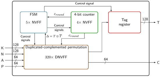
Figure 7.
System architecture.
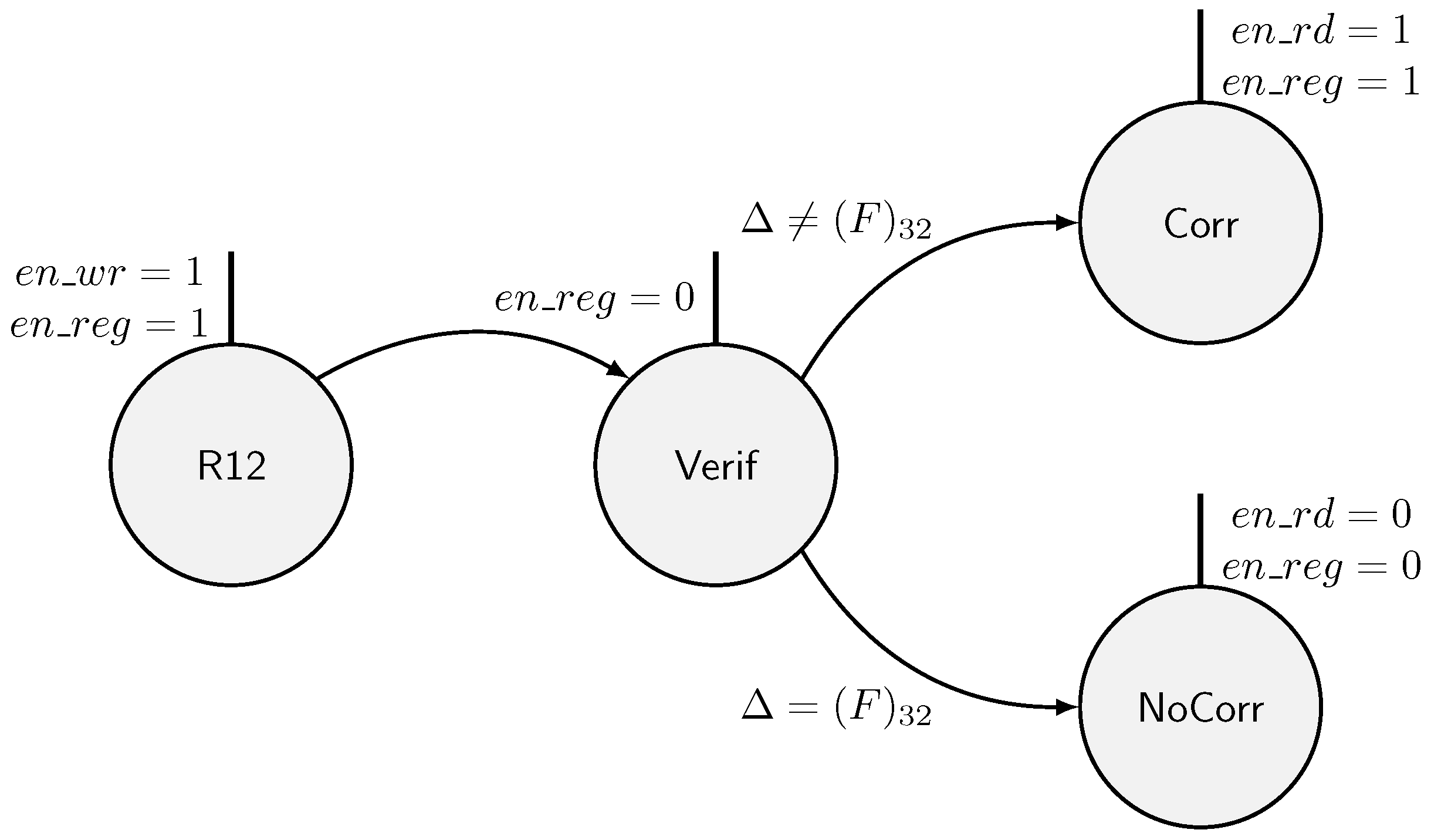
Fault correction mechanism is handled by the FSM. It requires three additional states as depicted in Figure 8. The first state checks if faults were injected in the last round (R12). In such a case, MTJs are read and the state is corrected. To correct the state, an extra clock cycle is necessary. The computation time of an encryption with state correction is then different from the computation time of an encryption without state correction. This difference in computation time could be used by an attacker to discriminate ineffective faults from effective faults. To avoid that, a dummy state (NoCorr) is introduced. During the verification and the noncorrection steps, the intermediate state registers are disabled (see Figure 9).
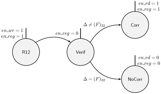
Figure 8.
FSM states managing the fault correction mechanism.
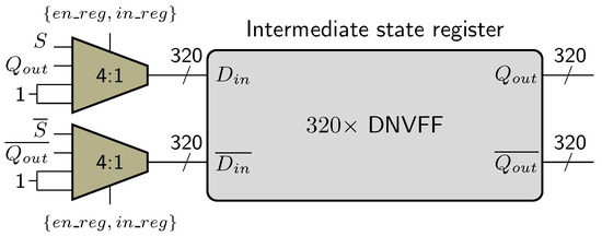
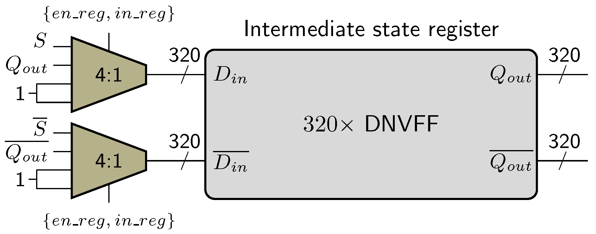
Figure 9.
Intermediate state registers overview.
The power consumption of a logic gate is directly related to the switching activity. An output transition from 0 to 1 is more power consuming than a transition from 1 to 0, from 0 to 0 or from 1 to 1. This difference in power consumption is exploited during side-channel analysis to reveal the secret key. As a remainder, DPA and CPA on Ascon are conducted at the end of the first round in the Initialization stage. To enhance the robustness of the circuit towards power analysis attacks, we suggest to charge all DNVFF outputs to ‘1’ at the beginning of the encryption, as illustrated in Figure 9. When DNVFFs are updated at the end of the first round, either output Q or output makes a transition from 1 to 0. This approach is similar to the one employed in the Wave Dynamic Differential Logic (WDDL) [25]. WDDL implements standard cells by pairs so that at any step of the computation, one and only one of the two gates switches.
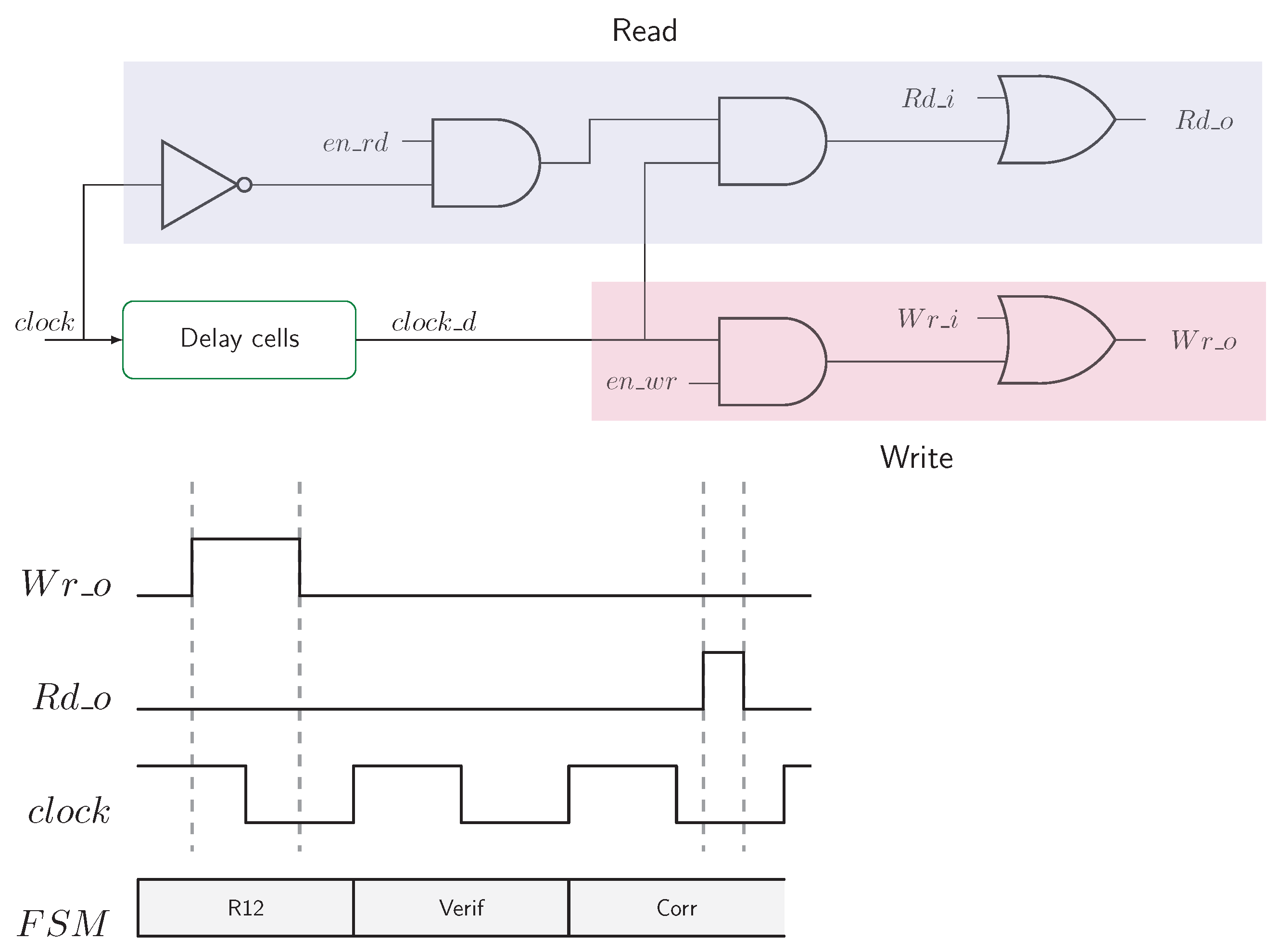
As stated earlier, the read operation cannot be enabled when the clock signal is high. In the same way, all the DNVFF outputs must be stable before being written into the MTJs. An incorrect generation of read and write pulses could induce timing violations, causing a circuit malfunction. To this end, we have developed a dedicated control circuit using delay cells. It is represented in Figure 10. The write signal is shifted to ensure that all registers are updated before writing the penultimate round into MTJs. Regarding the read operation, a short but sufficient pulse is generated between a falling and a rising edge of the clock. Pins denoted as Wr_i and Rd_i are external pins, used to save the context before a power-off phase. Note that this circuit is shared with all DNVFFs.
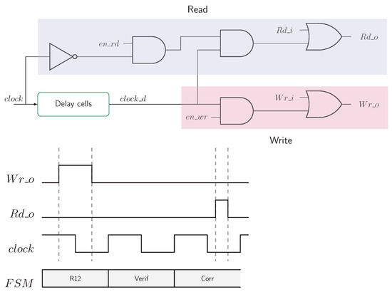
Figure 10.
Write/Read control circuit.
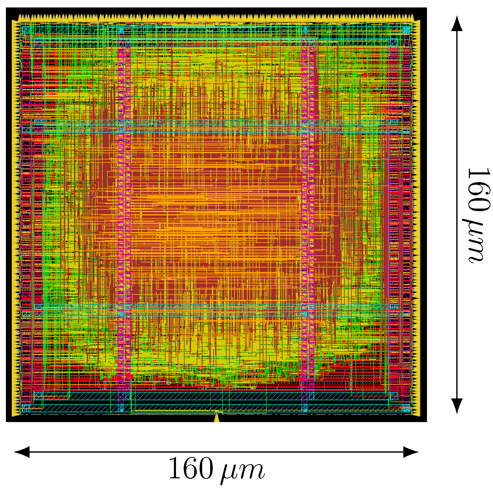
The ASIC design flow adopted to synthesize, place and route the design is described in Table 3. Special regards must be given during the synthesis. The synthesis tool tends to over-optimize the design to enhance timing, resulting in unbalanced dual-rail implementations. To solve the problem out, we applied a “bottom-up” strategy. This approach consists of synthesizing all submodules separately, starting from the lowest hierarchy level and proceeding up until the top-level design is compiled. During the placement routing, we precluded the tool from removing delay cells introduced in the circuit (Figure 10). The obtained layout of the protected version of Ascon is depicted in Figure 11. The floorplan dimension was fixed to m by m. We have conducted several timing analysis to confirm the functionality of the proposed countermeasure under different process, voltage, and temperature conditions.
Table 3.
ASIC design environment.
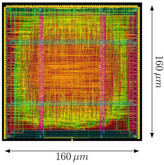
Figure 11.
Layout of the protected implementation of Ascon.
To assess the impact of the proposed countermeasure in terms of area and power consumption, we also designed, in parallel, an unprotected CMOS version of Ascon. Table 4 reports the area overhead of the countermeasure, for each submodule, in terms of and Gate Equivalent (GE). GE is computed using the smallest NAND2 gate in the ST DK. This unit is commonly used to specify the technology-independent complexity of digital electronic circuits (). As a remainder, we provide an area estimation as we did not draw the full layout of the DNVFF. The area overhead of the proposed countermeasure is compared to an unprotected version of Ascon. The hardware cost of the Write/Read control circuit (Figure 10) is not significant as it is shared across the circuit. Regarding the power consumption, the unprotected version consumes mW for one encryption, whereas the protected version consumes mW, representing an increase of .
Table 4.
Area requirements for both unprotected and protected designs.
If the throughput is still unchanged compared to the unprotected Ascon version, we need one more clock cycle to verify the tag T and its complemented value —and correct the tag T if a fault was occured—before ending the finalization process.
As mentioned previously, the proposed implementation is able to save the current state and the algorithm progression into the memory. In case of power loss, data can be reloaded, preventing a full algorithm re-computation. To be more energy efficient, the energy required to save and restore information must be lower than the energy wasted due to power failure plus the energy required to recompute lost data. In other words, in case of power failure, the proposed implementation is more energy efficient than a pure CMOS architecture when:
Table 5 sums up the energy comparison between both implementations in case of power loss at the end of algorithm stages. The proposed architecture offers energy reduction ranging from 11% to 32.5% compared to a duplicated-complemented CMOS version.
Table 5.
Energy consumption for one encryption in case of power failure during initialization and associated data phases.
Compared to existing countermeasures, our architecture has a lower area overhead than [17] (), but has a higher area overhead than [18] (). However, the countermeasure of [18] does not enhance the robustness against side-channel attacks, and does not offer the possibility to restart from last backup point in case of power failure.
5. Security Evaluation
5.1. Simulation Flow for Fault-Based Attacks
The security assessment is done through fault attack simulations on the post-route netlists. To inject faults in round computation, a dedicated testbench has been developed, using the and statements of the SystemVerilog language [26]. This testbench allows us to specify the targeted fault model, for one or several bits, at any time in the computation, everywhere in the design. Input vectors are generated with a Python version of Ascon. The results are stored in files for each S-Box or pair of S-Boxes targeted. The cryptanalysis for both SIFA and SSFA is conducted with Python scripts. Equations are solved using a CryptoMiniSat5 solver [27]. The related package for Python can be retrieved here (https://github.com/msoos/cryptominisat, accessed on 1 September 2024). All scripts are fully automated.
To make simulations more realistic, we have reproduced the effects of missed faults, successful but ineffective faults, and successful and effective faults observed with a clock glitch attack in [12]. Missed faults correspond to the case where an attacker did not manage to alter the execution of the encryption. Successful but ineffective faults refers to the scenario where an attacker successfully disturbs the execution, but no effect is observed in the outcome of the encryption. On the contrary, the computation is affected with successful and effective faults attacks. For SIFA, the bias observed results in the combination of successful but ineffective faults and missed faults. For SSFA, missed faults heightens the number of encryption required to reveal the secret key. To create missed faults, we set the probability of fault injection to 70%. This rate is relevant for the CMOS 28 nm technology node [28].
As specified in Section 2, the key is divided into words of n bits. For all our experiments, we have fixed n to 64, thus implying to target 62 pairs of S-Boxes for SIFA and 63 S-Boxes for SSFA. We have conducted 1000 encryptions for each target.
5.2. SIFA
We have considered several use cases to evaluate the effectiveness of the countermeasure under different fault models:
- Case #1: Bit-reset on bits for each pair of S-Boxes ;
- Case #2: Bit-set on bits for each pair of S-Boxes ;
- Case #3 (protected version only): Bit-reset on bits for each pair of S-Boxes ;
- Case #4 (protected version only): Bit-reset on bits and bit-set on bits for each pair of S-Boxes .
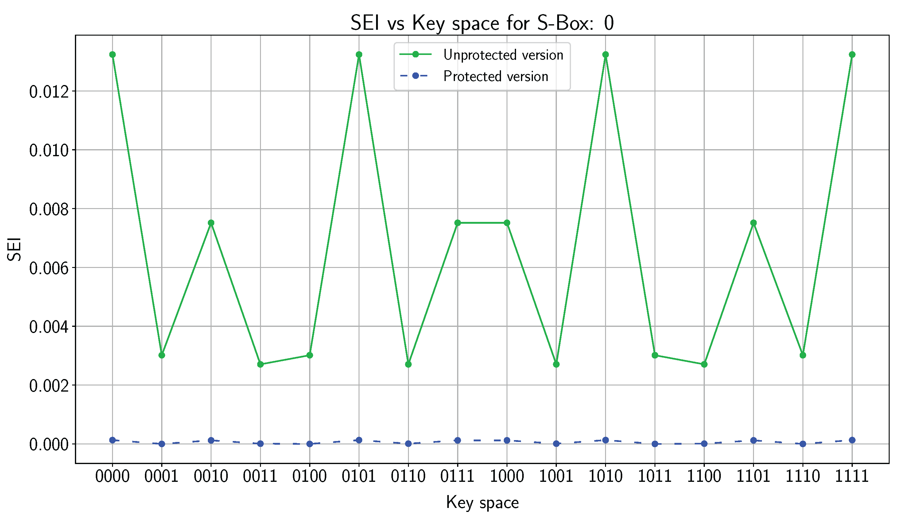
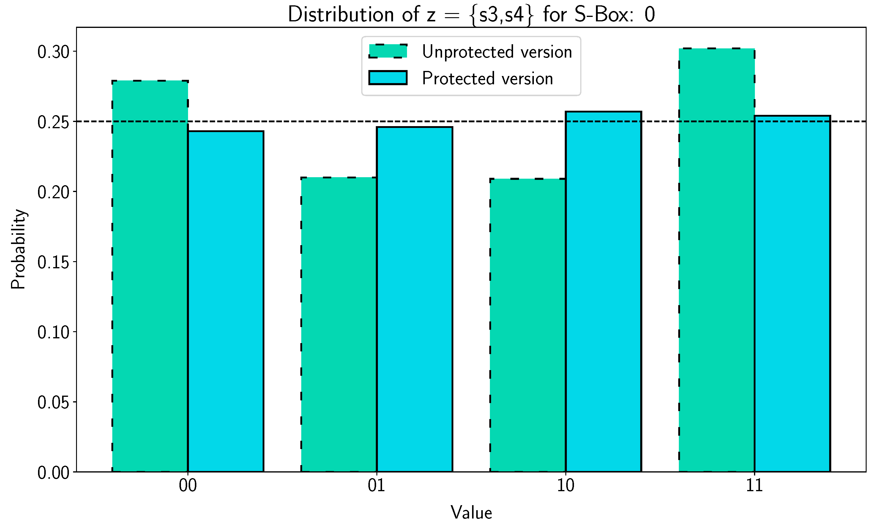
Figure 12 represents the fault distribution probability density of S-Box 0 for case #1 for both the unprotected version and protected version. Corresponding SEI values are displayed on Figure 13. On the protected implementation, for 1000 encryptions, we have obtained 1000 correct tags. Therefore, any bias can be observed on the fault distribution of Figure 12 (blue histogram). On the unprotected architecture, over 1000 encryptions, 346 correct tags (ineffective faults and missed faults) have been retrieved. A significant bias is observed on the fault distribution of Figure 12 (green histogram). The orders of magnitude of the for the protected and unprotected version are and , respectively. The low values of obtained with protected version mean that the fault distribution is close to a uniform distribution.
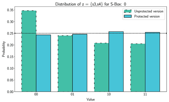
Figure 12.
SIFA Case #1: Fault distribution for S-Box 0 for protected version (blue) and unprotected version (green).
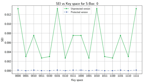
Figure 13.
Case #1: versus key search space for S-Box 0 for protected version (blue) and unprotected version (green).
Table 6 summarizes the results for each case on both the unprotected and protected version of the cipher. The result for the case #4 is not very surprising. Even though all bits are attacked in a complementary way, the relation remains valid, meaning there is no state correction. Although this scenario is theoretically possible, it seems irreproducible in practice given that it would require to inject four faults at four different locations, in a complementary manner. At the best of our knowledge, no attack using this fault model has been proposed in the literature. In conclusion, the proposed countermeasure completely removes the significant bias introduced by fault injections, preventing an attacker to recover the key by SIFA.
Table 6.
SIFA summary for each case.
5.3. SSFA
In the same vein, we have considered multiple attack scenarios:
- Case #1: Bit-reset on input bit of each S-Box j;
- Case #2 (protected version only): Bit-reset on input bits of each S-Box j;
- Case #3 (protected version only): Bit-reset on input bit and bit-set on input bit of each S-Box j.
The resulting fault distribution for the case #1 is depicted in Figure 14. For 1000 encryptions, we extracted 0 faulty tags on the protected implementation, whereas we retrieved 368 faulty tags on the unprotected implementation. For the protected version, the bias is completely removed from the fault distribution of Figure 14 (blue histogram). For the unprotected version, a significant bias can be observed on the fault distribution of Figure 14 (green histogram). The results for each case are summed up in Table 7. Similar behavior can be observed for the SSFA. Once again, the case #3 seems unfeasible in practical experiments. To conclude, the proposed architecture completely removes the bias induced by fault injections, making it impossible to retrieve the secret key by means of SSFA.
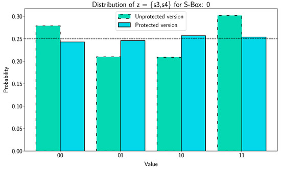
Figure 14.
SSFA Case #1: Fault distribution for S-Box 0 for the protected version (blue) and unprotected version (green).
Table 7.
SSFA summary for each case.
5.4. Power Analysis Attacks
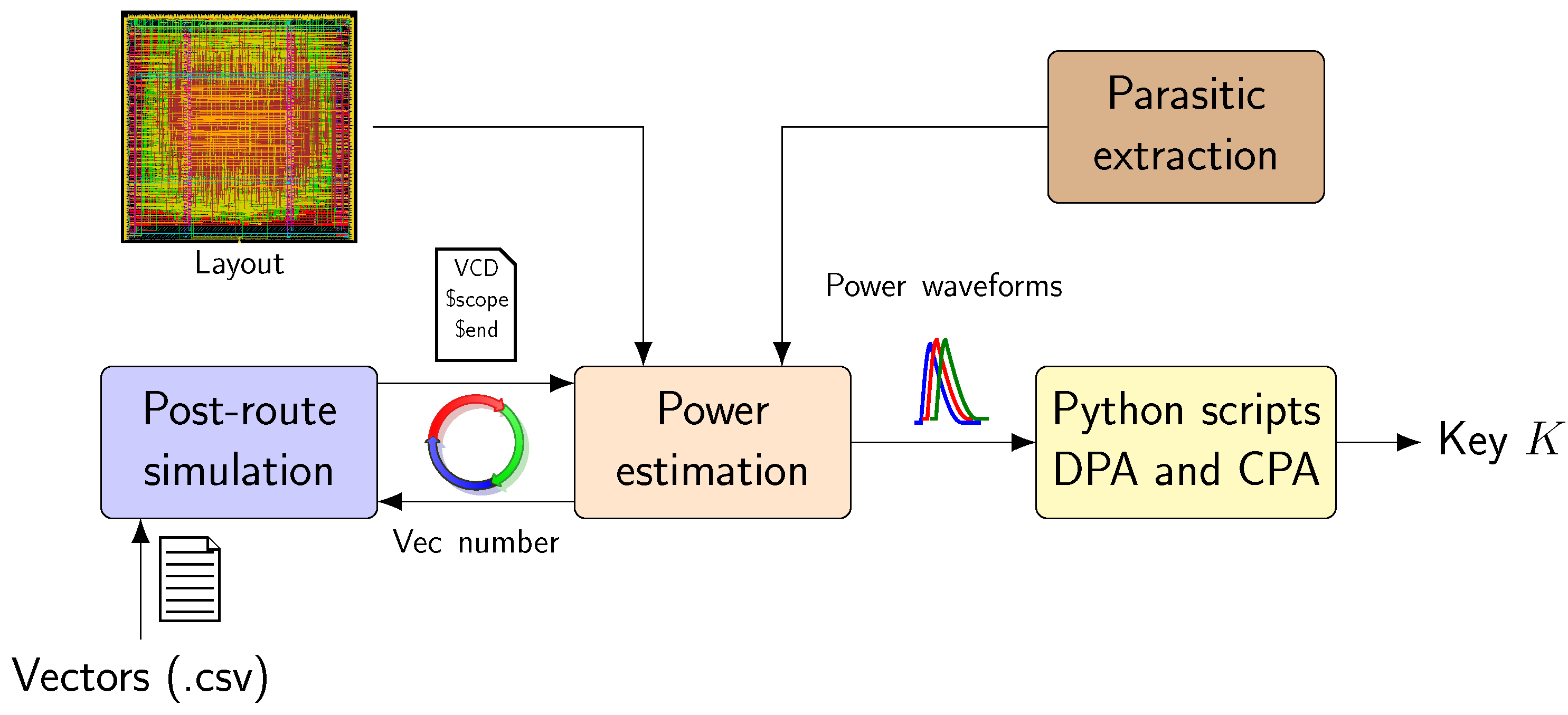
A power analysis evaluation needs a consequent set of power traces. Generating this set by means of transistor-level simulations is unrealistic, as it would require significant time resources. Thus, we rather use a power estimation tool (Cadence Voltus). Figure 15 shows the simulation flow adopted to carry out side-channel attacks. Power waveforms are computed from the physical layout of the circuit. Switching activities are stored in VCD files. These files are generated on-the-fly thanks to logical simulations. A similar flow has already been presented in the literature [29].
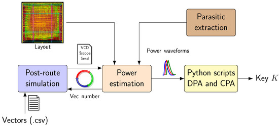
Figure 15.
Side-channel analysis with ASIC design flow.
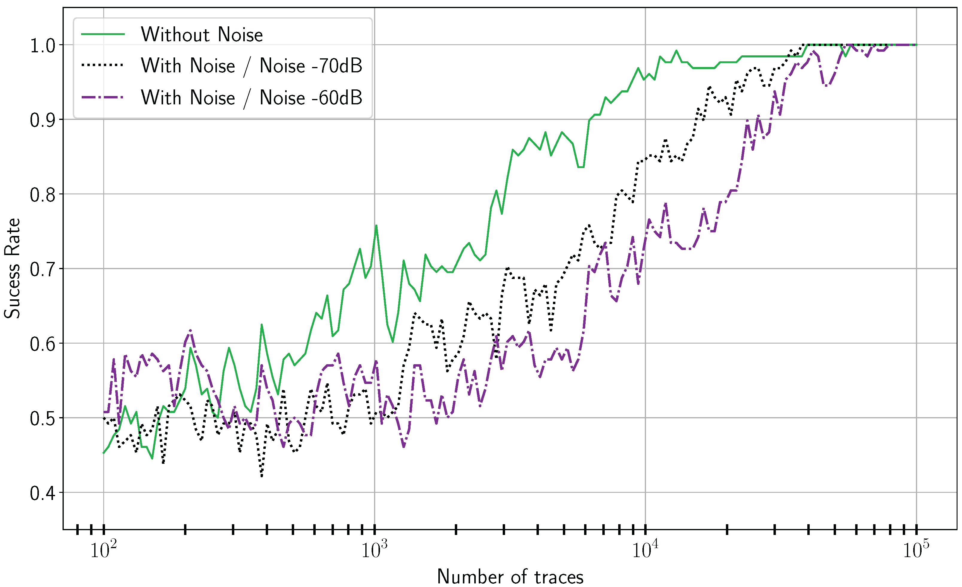
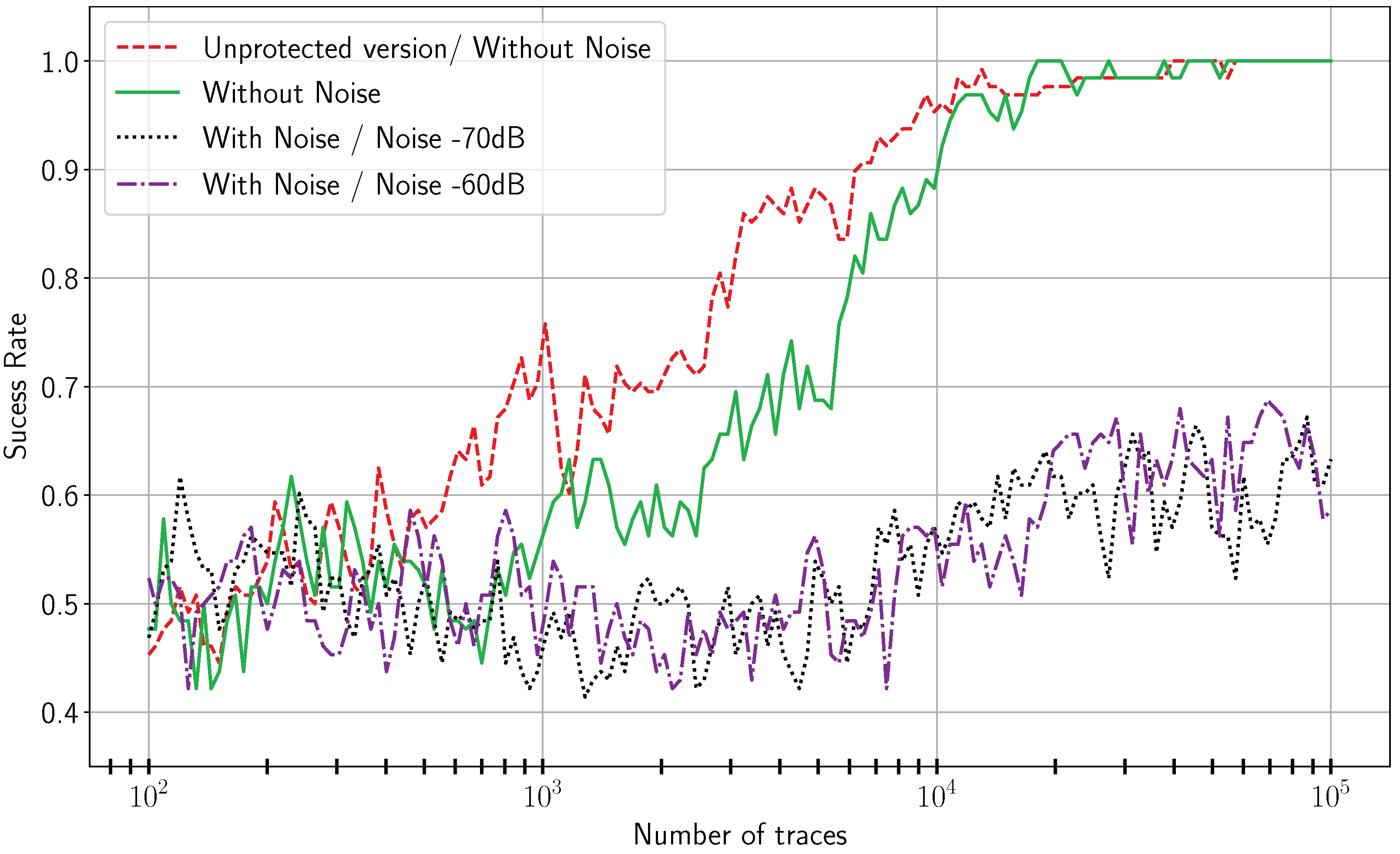
The cryptanalysis is performed with Python scripts. For all analysis, we have plotted the success rate versus the number of power traces. In our simulations, we consider the attack successful if we manage to retrieve all key bits (). However, it would be possible to recover last key bits by exhaustive research for in a reasonable time. We used a Hamming Weight (HW) as model to conduct CPA. The sampling rate is fixed at 1 ns. Timing window is fixed at 10 ns, the duration of one clock period. Thus, each power waveform contains 10 sample points per clock cycle. Additive Gaussian White Noise has been added on power signals to take into account impact of ambient noise on the success rate. In practical experiments, this noise could be generated for instance by measurement devices. Noise levels are fixed at dB and dB. To enhance the script efficiency, Pearson Correlation is calculated in an incremental fashion using the formula from [30]. To further decrease the computation time, all intermediate variables and HW are pre-computed. The power analysis is performed over 100,000 power traces for both protected and unprotected version.
Figure 16 and Figure 17, respectively, represent the success rates for CPA on unprotected and protected implementations. Without noise, all key bits can be recovered regardless the architecture. The leakage is not completely removed in the protected version as cell interconnections are not equally sized, resulting in unbalanced capacitance loads in dual-rail [31]. That is why it remains possible to recover the key with CPA. Nonetheless, in presence of noise, it is impossible to extract key bits on the protected implementation with 100,000 traces.
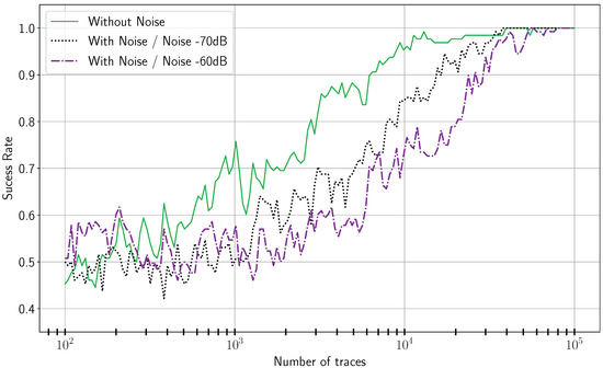
Figure 16.
CPA on the unprotected implementation.
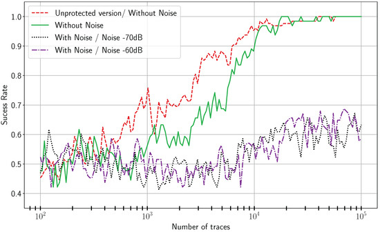
Figure 17.
CPA on the proposed implementation.
Regarding DPA, the results are depicted in Figure 18 and Figure 19. On the unprotected implementation, the secret key can be retrieved with or without noise. On the contrary, even with 100,000 power traces, the secret key is uncovered on the proposed architecture. In conclusion, our countermeasure significantly increases the number of traces required to recover the secret key with DPA.
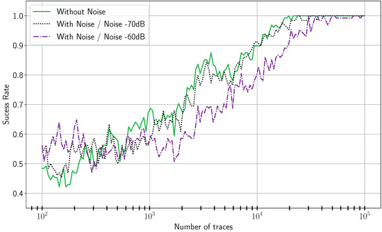
Figure 18.
DPA on the unprotected implementation.
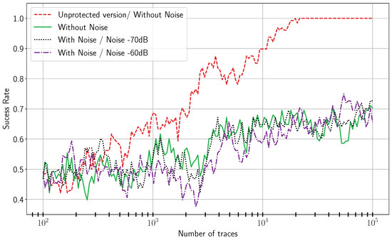
Figure 19.
DPA on the proposed implementation.
6. Discussion
As demonstrated in the previous section, our countermeasure is efficient to protect Ascon from both SIFA and SSFA. The bias introduced by fault injection attacks are removed by correcting the state. When the state is not corrected, no difference in power consumption is induced. However, an additional energy () is required to read MTJs when the state need to be corrected. From this observation, one could hypothesize that an attacker could be able to know when there is a state correction by monitoring the power consumption of the device. Measuring the power consumption of a device undergoing a fault-based attack is difficult. Fault injection equipments could interfere with probe measurement, making the power measurement unreliable. This attack scenario seems unlikely.
In addition, the countermeasure could become ineffective if the state registers, i.e., the DNVFFs, are attacked during the writing operation. To the best of our knowledge, no attack was presented in the literature that specifically targets the intermediate state register. Nevertheless, if this scenario occurs, one solution could be to save the state two rounds before the tag computation. This would increase the encryption time by only one clock period compared to the current circuit. A fault injection in 10th round of the Finalization phase is not exploitable due to the diffusion feature of Ascon.
In [32], C. Dobraunig et al. conducted an SIFA attack during the Initialization stage of the decryption process of Ascon. The countermeasure proposed in this work could be tailored to also cover this attack scenario. A correction of the intermediate state could be performed during the Initialization phase. To do so, it would be necessary to introduce new states in the FSM, as depicted in Figure 8.
Finally, one could wonder if data stored in MTJs can remain secure under fault injection. In [33], the authors demonstrated that information stored in the memory can be altered if the MTJ is illuminated by a laser beam during 1 s. This time duration is relatively high compared to the encryption time. On top of that, CMOS will be highly sensitive to a laser pulse of 1 s, thus creating a significant number of fault in the computation. Performing SIFA and SSFA by attacking MTJs is then unfeasible. Nonetheless, ref. [33] have also shown that for a laser power of mW and a laser pulse of s, MTJ cells pass into a degradation region, where P and AP states have different resistance values. This could disrupt reading circuit of the DNVFF, thus inducing persistent faults in the computation. In such a case, Persistent Fault Analysis (PFA) [34] and Statistical Ineffective Persistent Faults Analysis (SIPFA) [35] could become possible. We leave this problem open for future research.
7. Conclusions
In this work, we focused on the CMOS/MRAM hybridization and the Ascon authenticated cipher. We presented a countermeasure against fault-based attacks and side-channel attacks. The basic idea is to correct all faults introduced in the algorithm computation caused by fault injection attacks. To detect faults, we duplicated and complemented the permutation of Ascon. The fault correction is based on DNVFFs. These DNVFFs are composed of two CMOS FF and a nonvolatile circuit. The nonvolatily is used to perform write and read operations of MTJ cells. In the penultimate round of each encryption, the state is stored into MTJ cells. When a fault is detected, MTJs cells are read and the state is corrected. We precisely detailed how to implement this countermeasure within a hardware implementation of Ascon. Compared to a reference implementation, the area overhead of the proposed architecture is . For the power consumption aspect, the countermeasure can save up to 32.5% energy in case of power failure compared to a naïve duplicated-complemented Ascon.
The security analysis was done through fault attack and power analysis simulations. To this end, we developed a simulation flow using existing EDA tools. In the fault analysis experiments, the countermeasure completely removes the statistical bias introduced by ineffective and effective faults. We showed that it is impossible to reveal the secret key with SIFA and SSFA. Regarding side-channel attacks, our countermeasure enhances the robustness of the circuit against DPA. In addition, our countermeasure makes it more difficult to recover secret information by means of CPA.
Our case of study is based on Ascon and STT-MRAM. It could be interesting to apply the principle of our countermeasure to other emerging nonvolatile memories, such as Ferroelectric Field-Effect Transistor [36], Phase Change Memory [37], or Resistive Random Access Memory [38]. As these memories have different characteristics, the performance could be enhanced or degraded compared to our MRAM-based countermeasure. The countermeasure could also be adopted to other lightweight ciphers, such as PRESENT [19].
Author Contributions
Conceptualization, N.R., O.P., J.-M.D. and J.-B.R.; Methodology, N.R.; Validation, G.D.P.; Writing—original draft, N.R.; Writing—review & editing, N.R., O.P., G.D.P., J.-M.D. and J.-B.R.; Supervision, O.P., J.-M.D. and J.-B.R.; Project administration, J.-B.R. All authors have read and agreed to the published version of the manuscript.
Funding
This research was funded by the Agence Nationale de la Recherche grant number ANR-19-CE39-0010.
Data Availability Statement
Data are contained within the article.
Conflicts of Interest
The authors declare no conflicts of interest.
Abbreviations
The following abbreviations are used in this manuscript:
| AP | Antiparallel |
| ASIC | Application Specific Integrated Circuit |
| CMOS | Complementary Metal Oxide Semiconductor |
| CPA | Correlation Power Analysis |
| DK | Design Kit |
| DNVFF | Differential Nonvolatile Flip-Flop |
| DPA | Differential Power Analysis |
| EDA | Electronic Design Automation |
| FM | Ferromagnetic |
| FSM | Finite State Machine |
| GE | Gate Equivalent |
| HW | Hamming Weight |
| IoT | Internet of Things |
| LWC | Lightweight Cryptography |
| MRAM | Magnetic Random Access Memory |
| MTJ | Magnetic Tunnel Junction |
| NIST | National Institute of Standards and Technology |
| NVFF | Nonvolatile Flip-Flop |
| P | Parallel |
| SEI | Squared Euclidean Imbalance |
| SR | Success Rate |
| SIFA | Statistical Ineffective Fault Analysis |
| SSFA | Subset Fault Analysis |
| TMR | Tunnel Magnetoresistance Ratio |
| WDDL | Wave Dynamic Differential Logic |
References
- Alioto, M.; Shahghasemi, M. The Internet of Things on Its Edge: Trends Toward Its Tipping Point. IEEE Consumer Electron. Mag. 2018, 7, 77–87. [Google Scholar] [CrossRef]
- NIST FIPS PUB 197; Advanced Encryption Standard (AES). National Institute of Standards and Technology, U.S. Department of Commerce: Gaithersburg, MD, USA, 2001.
- Dobraunig, C.; Eichlseder, M.; Mendel, F.; Schläffer, M. Ascon v1.2: Lightweight Authenticated Encryption and Hashing. J. Cryptol. 2021, 34, 33. [Google Scholar] [CrossRef]
- Bernstein, D.J. CAESAR Competition. 2014. Available online: https://competitions.cr.yp.to/index.html (accessed on 1 September 2024).
- Samwel, N.; Daemen, J. DPA on hardware implementations of Ascon and Keyak. In Proceedings of the Computing Frontiers Conference, CF’17, Siena, Italy, 15–17 May 2017; ACM: New York, NY, USA, 2017; pp. 415–424. [Google Scholar] [CrossRef]
- Ramezanpour, K.; Ampadu, P.; Diehl, W. FIMA: Fault Intensity Map Analysis; Springer: Cham, Switzerland, 2019; pp. 63–79. [Google Scholar] [CrossRef]
- Joshi, P.; Mazumdar, B. SSFA: Subset fault analysis of ASCON-128 authenticated cipher. Microelectron. Reliab. 2021, 123, 114155. [Google Scholar] [CrossRef]
- Sanislav, T.; Mois, G.D.; Zeadally, S.; Folea, S.C. Energy Harvesting Techniques for Internet of Things (IoT). IEEE Access 2021, 9, 39530–39549. [Google Scholar] [CrossRef]
- Dieny, B.; Prejbeanu, I.L.; Garello, K.; Gambardella, P.; Freitas, P.; Lehndorff, R.; Raberg, W.; Ebels, U.; Demokritov, S.O.; Akerman, J.; et al. Opportunities and challenges for spintronics in the microelectronics industry. Nat. Electron. 2020, 3, 446–459. [Google Scholar] [CrossRef]
- Roussel, N.; Potin, O.; di Pendina, G.; Dutertre, J.; Rigaud, J. CMOS/STT-MRAM Based Ascon LWC: A Power Efficient Hardware Implementation. In Proceedings of the 29th IEEE International Conference on Electronics, Circuits and Systems, ICECS 2022, Glasgow, UK, 24–26 October 2022; IEEE: New York, NY, USA, 2022; pp. 1–4. [Google Scholar] [CrossRef]
- Ramezanpour, K.; Ampadu, P.; Diehl, W. A Statistical Fault Analysis Methodology for the Ascon Authenticated Cipher. In Proceedings of the IEEE International Symposium on Hardware Oriented Security and Trust, HOST 2019, McLean, VA, USA, 5–10 May 2019; IEEE: New York, NY, USA, 2019; pp. 41–50. [Google Scholar] [CrossRef]
- Dobraunig, C.; Eichlseder, M.; Korak, T.; Mangard, S.; Mendel, F.; Primas, R. SIFA: Exploiting Ineffective Fault Inductions on Symmetric Cryptography. IACR Trans. Cryptogr. Hardw. Embed. Syst. 2018, 2018, 547–572. [Google Scholar] [CrossRef]
- Tezcan, C. Truncated, Impossible, and Improbable Differential Analysis of ASCON. In Proceedings of the 2nd International Conference on Information Systems Security and Privacy, ICISSP 2016, Rome, Italy, 19–21 February 2016; Camp, O., Furnell, S., Mori, P., Eds.; SciTePress: Lisbon, Portugal, 2016; pp. 325–332. [Google Scholar] [CrossRef]
- Kocher, P.C.; Jaffe, J.; Jun, B. Differential Power Analysis; Springer: Berlin/Heidelberg, Germany, 1999; pp. 388–397. [Google Scholar] [CrossRef]
- Brier, E.; Clavier, C.; Olivier, F. Correlation Power Analysis with a Leakage Model; Springer: Berlin/Heidelberg, Germany, 2004; pp. 16–29. [Google Scholar] [CrossRef]
- Kharbouche-Harrari, M.; di Pendina, G.; Wacquez, R.; Dieny, B.; Aboulkassimi, D.; Postel-Pellerin, J.; Portal, J. Light-Weight Cipher Based on Hybrid CMOS/STT-MRAM: Power/Area Analysis. In Proceedings of the IEEE International Symposium on Circuits and Systems, ISCAS 2019, Sapporo, Japan, 26–29 May 2019; IEEE: New York, NY, USA, 2019; pp. 1–5. [Google Scholar] [CrossRef]
- Saha, S.; Jap, D.; Roy, D.B.; Chakraborty, A.; Bhasin, S.; Mukhopadhyay, D. A Framework to Counter Statistical Ineffective Fault Analysis of Block Ciphers Using Domain Transformation and Error Correction. IEEE Trans. Inf. Forensics Secur. 2020, 15, 1905–1919. [Google Scholar] [CrossRef]
- Baksi, A.; Kumar, V.B.Y.; Karmakar, B.; Bhasin, S.; Saha, D.; Chattopadhyay, A. A Novel Duplication Based Countermeasure to Statistical Ineffective Fault Analysis; Springer: Cham, Switzerland, 2020; pp. 525–542. [Google Scholar] [CrossRef]
- Bogdanov, A.; Knudsen, L.R.; Leander, G.; Paar, C.; Poschmann, A.; Robshaw, M.J.B.; Seurin, Y.; Vikkelsoe, C. PRESENT: An Ultra-Lightweight Block Cipher; Springer: Berlin/Heidelberg, Germany, 2007; pp. 450–466. [Google Scholar] [CrossRef]
- Jabeur, K.; Bernard-Granger, F.; Di Pendina, G.; Prenat, G.; Dieny, B. Comparison of Verilog-A compact modelling strategies for spintronic devices. Electron. Lett. 2014, 50, 1353–1355. [Google Scholar] [CrossRef]
- Prenat, G.; Jabeur, K.; Vanhauwaert, P.; di Pendina, G.; Oboril, F.; Bishnoi, R.; Ebrahimi, M.; Lamard, N.; Boulle, O.; Garello, K.; et al. Ultra-Fast and High-Reliability SOT-MRAM: From Cache Replacement to Normally-Off Computing. IEEE Trans. Multi Scale Comput. Syst. 2016, 2, 49–60. [Google Scholar] [CrossRef]
- Coi, O.; Pendina, G.; Prenat, G.; Torres, L. Spin-Transfer Torque Magnetic Tunnel Junction for Single-Event Effects Mitigation in IC Design. IEEE Trans. Nucl. Sci. 2020, 67, 1674–1681. [Google Scholar] [CrossRef]
- Goodstein, R. Boolean Algebra; Dover Books on Mathematics; Dover Publications: Mineola, NY, USA, 2012. [Google Scholar]
- Groß, H.; Wenger, E.; Dobraunig, C.; Ehrenhöfer, C. Ascon hardware implementations and side-channel evaluation. Microprocess. Microsyst. 2017, 52, 470–479. [Google Scholar] [CrossRef]
- Tiri, K.; Verbauwhede, I. A Logic Level Design Methodology for a Secure DPA Resistant ASIC or FPGA Implementation. In Proceedings of the 2004 Design, Automation and Test in Europe Conference and Exposition (DATE 2004), Paris, France, 16–20 February 2004; IEEE Computer Society: Washington, DC, USA, 2004; pp. 246–251. [Google Scholar] [CrossRef]
- IEEE STD 1800-2009; IEEE Standard for SystemVerilog–Unified Hardware Design, Specification, and Verification Language. IEEE: Piscataway, NJ, USA, 2009; pp. 1–1285. [CrossRef]
- Soos, M.; Nohl, K.; Castelluccia, C. Extending SAT Solvers to Cryptographic Problems. In International Conference on Theory and Applications of Satisfiability Testing, Proceedings of the 12th International Conference, SAT 2009, Swansea, UK, 30 June–3 July 2009; Lecture Notes in Computer Science; Kullmann, O., Ed.; Springer: Berlin/Heidelberg, Germany, 2009; Volume 5584, pp. 244–257. [Google Scholar] [CrossRef]
- Dutertre, J.; Beroulle, V.; Candelier, P.; Castro, S.D.; Faber, L.; Flottes, M.; Gendrier, P.; Hély, D.; Leveugle, R.; Maistri, P.; et al. Laser Fault Injection at the CMOS 28 nm Technology Node: An Analysis of the Fault Model. In Proceedings of the 2018 Workshop on Fault Diagnosis and Tolerance in Cryptography, FDTC 2018, Amsterdam, The Netherlands, 13 September 2018; IEEE Computer Society: Washington, DC, USA, 2018; pp. 1–6. [Google Scholar] [CrossRef]
- Park, J.; Anandakumar, N.N.; Saha, D.; Mehta, D.; Pundir, N.; Rahman, F.; Farahmandi, F.; Tehranipoor, M.M.; PQC-SEP: Power Side-Channel Evaluation Platform for Post-Quantum Cryptography Algorithms. Cryptology ePrint Archive, Paper 2022/527. 2022. Available online: https://eprint.iacr.org/2022/527 (accessed on 1 September 2024).
- Bottinelli, P.; Bos, J.W. Computational aspects of correlation power analysis. J. Cryptogr. Eng. 2017, 7, 167–181. [Google Scholar] [CrossRef]
- Guilley, S.; Chaudhuri, S.; Sauvage, L.; Graba, T.; Danger, J.L.; Hoogvorst, P.; Vong, V.N.; Nassar, M.; Flament, F. Shall we trust WDDL? In Future of Trust in Computing, Proceedings of the First International Conference Future of Trust in Computing 2008, Villach, Austria, 11–12 March 2008; Vieweg+Teubner: Wiesbaden, Germany, 2009; pp. 208–215. [Google Scholar] [CrossRef]
- Dobraunig, C.; Mangard, S.; Mendel, F.; Primas, R. Fault Attacks on Nonce-Based Authenticated Encryption: Application to Keyak and Ketje; Springer: Cham, Switzerland, 2019; pp. 257–277. [Google Scholar] [CrossRef]
- Yazigy, N.; Postel-Pellerin, J.; Marca, V.D.; Sousa, R.C.; Ribotta, A.L.; Pendina, G.D.; Canet, P. Real-time electrical measurements during laser attack on STT-MRAM. In Proceedings of the 2023 35th International Conference on Microelectronic Test Structure (ICMTS), Tokyo, Japan, 27–30 March 2023; pp. 1–6. [Google Scholar] [CrossRef]
- Zhang, F.; Lou, X.; Zhao, X.; Bhasin, S.; He, W.; Ding, R.; Qureshi, S.; Ren, K. Persistent Fault Analysis on Block Ciphers. IACR Trans. Cryptogr. Hardw. Embed. Syst. 2018, 2018, 150–172. [Google Scholar] [CrossRef]
- Bagheri, N.; Sadeghi, S.; Ravi, P.; Bhasin, S.; Soleimany, H. SIPFA: Statistical Ineffective Persistent Faults Analysis on Feistel Ciphers. IACR Trans. Cryptogr. Hardw. Embed. Syst. 2022, 2022, 367–390. [Google Scholar] [CrossRef]
- Marchand, C.; O’Connor, I.; Cantan, M.; Breyer, E.T.; Slesazeck, S.; Mikolajick, T. FeFET based Logic-in-Memory: An overview. In Proceedings of the 16th International Conference on Design & Technology of Integrated Systems in Nanoscale Era, DTIS 2021, Montpellier, France, 28–30 June 2021; IEEE: New York, NY, USA, 2021; pp. 1–6. [Google Scholar] [CrossRef]
- Khan, R.S.; Noor, N.; Jin, C.; Scoggin, J.; Woods, Z.; Muneer, S.; Ciardullo, A.; Nguyen, P.; Gokirmak, A.; van Dijk, M.; et al. Phase Change Memory and Its Applications in Hardware Security; CRC Press: Boca Raton, FL, USA, 2017; pp. 93–114. [Google Scholar] [CrossRef]
- Rajendran, G.; Banerjee, W.; Chattopadhyay, A.; Aly, M.M.S. Application of Resistive Random Access Memory in Hardware Security: A Review. Adv. Electron. Mater. 2021, 7, 2100536. [Google Scholar] [CrossRef]


Disclaimer/Publisher’s Note: The statements, opinions and data contained in all publications are solely those of the individual author(s) and contributor(s) and not of MDPI and/or the editor(s). MDPI and/or the editor(s) disclaim responsibility for any injury to people or property resulting from any ideas, methods, instructions or products referred to in the content. |
© 2024 by the authors. Licensee MDPI, Basel, Switzerland. This article is an open access article distributed under the terms and conditions of the Creative Commons Attribution (CC BY) license (https://creativecommons.org/licenses/by/4.0/).