1. Introduction
Since the invention of the automobile, road accidents and automotive vehicles have gone hand in hand. On 29 January 1886, Carl Benz applied for a patent for his “vehicle powered by a gas engine”, which may be regarded as the birth certificate of the automobile. Just a few years later, the first recorded gasoline car accident happened in Ohio in 1891.
Since then, various kinds of motor vehicles became a necessity in everyday life. The growing number of cars has exacerbated the road accident problem to the point where the UN General Assembly adopted resolution A/RES/74/299 on “Improving Global Road Safety”. This resolution established a target to reduce by at least 50% the number of road traffic deaths and injuries by 2030 [
1]. It is estimated that every year the lives of approximately 1.3 million people are cut short as a result of a road traffic crash. These types of traffic injuries are the leading cause of death for children [
2]. Most of these accidents happen in the areas around schools and playgrounds where a driver cannot respond fast enough to a child’s sudden appearance on the road.
The Advanced Driving Assistance System (ADAS) is a convenient option for increasing driving safety and reducing the number and severity of accidents [
3,
4]. These systems usually employ frequency-modulated continuous wave (FMCW) radar as a primary sensor. Radar sensors, unlike cameras, can operate in a variety of lighting and weather conditions, do not require a direct line of sight to the object, and can pass through optically opaque materials. A growing number of these systems feed processed radar data into a centralized processing unit (CPU). The CPU then runs a massive deep learning neural network to determine what is ahead of the vehicle and whether to brake or accelerate. Prior to feeding the data into this processing unit, the raw radar data are typically processed using some higher-order radar signal processing method [
5,
6]. For example, to obtain the distance and velocity information of the obstacles, Doppler fast Fourier transform (FFT) can be used. Depending on how the radar was set up and the Doppler-FFT implementation, the Doppler processing time can range from milliseconds to dozens of milliseconds. On the other hand, neural network inference typically takes much longer and can be measured in tens or even hundreds of milliseconds [
6,
7,
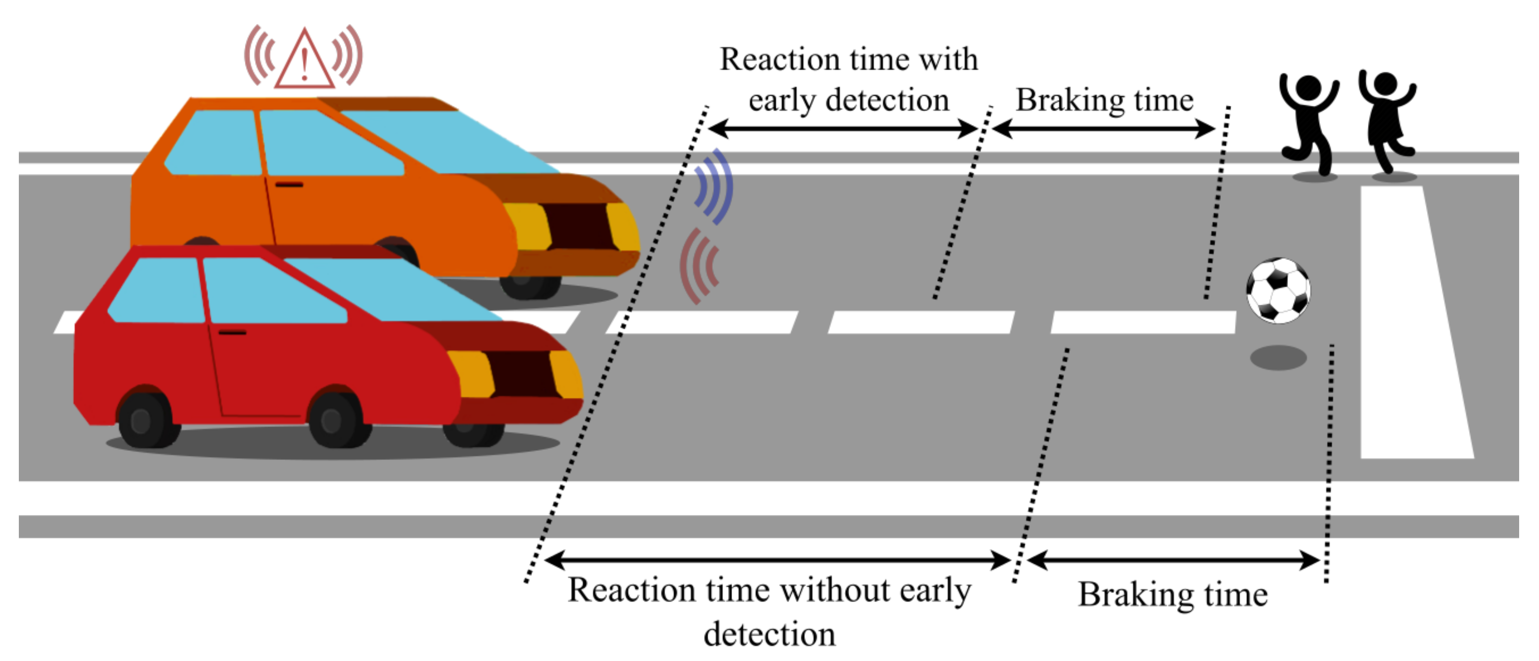
8]. Given the variety of sensors in modern automobiles, it is obvious that the CPU cannot make all decisions while still operating in real time. Instead, in order to avoid potential collisions (
Figure 1), the decision must be made at a low level very close to the sensor itself and distance information must be sent immediately without waiting for higher-order processing algorithms.
There is a number of low level range-Doppler-FFT hardware accelerators described in the scientific and technical literature that can determine whether an obstacle is present without invoking fully pledged CPU processing [
9,
10,
11,
12,
13]. These topologies typically do not account for nor report the time required to receive data from the radar front-end and assume that data are continuously streamed into the accelerator, which is not the case in most of the realistic automotive scenarios. As a result, the latencies of these systems may be overoptimistic. Furthermore, most of the proposed architectures are not flexible enough to accommodate a wide range of radar sensors employed in the automotive industry.
This manuscript presents a radar signal processing architecture for the early detection of automotive obstacles that does not impede subsequent higher-order processing and considers the time required to receive the data from the radar front-end. The proposed architecture was designed using the agile [
14] digital design methodology and it is written in the Chisel [
15] hardware design language. This architecture is suitable for interfacing with different types of automotive radar front-ends. It supports a collection of pipelined FFT processors with a plethora of parametrization options and six different variants of the CFAR algorithm.
The paper is organized as follows:
Section 2 gives a short overview of the FMCW radar front-end and back-end.
Section 3 presents the proposed hardware generator for early obstacle detection and an overview of each block in the system.
Section 4 presents a method for reducing the system latency and discusses the system limitations and the minimum achievable latency. In
Section 5, experimental results are demonstrated and finally,
Section 6 draws the conclusion.
2. Operating Principles of an FMCW Radar
Conventional automotive radar operates with a sequence of FMCW signals and is a well-studied research field [
4,
16,
17,
18]. The typical frequency bands for automotive radar are 24 and 77/79
, with most of the manufacturers shifting toward 77/79
for newer radar generations. This is due to the larger available bandwidth (76–77
for long-range and 77–81
for short-range applications), higher Doppler sensitivity (and thus higher velocity resolution), and smaller antennas [
19]. These types of radar can be classified depending on the measurement range: short-range radar (up to 50 m), mid-range radar (up to 100 m), and long-range radar (up to 250 m) [
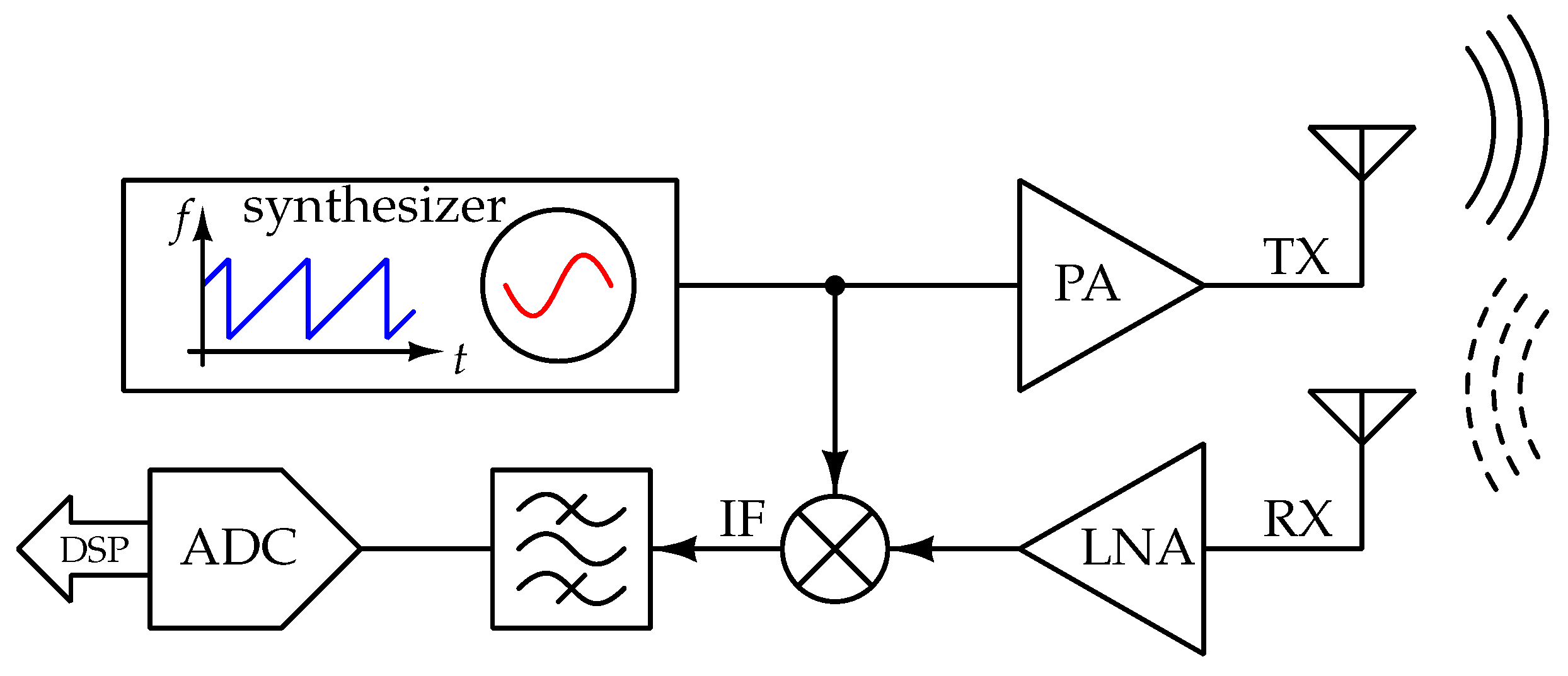
20]. A simplified block diagram of a typical FMCW radar front-end with Single-Input Single-Output (SISO) is given in
Figure 2.
These systems consist of a frequency synthesizer that generates a linear chirp/sweep. The generated chirp is amplified and then transmitted with the TX antenna. After the reflection off an object, the chirp is received at the RX antenna. The RX and the TX signals are mixed to produce the IF signal, resulting in a frequency proportional to the object distance and called the beat frequency. The beat frequency
is proportional to the round-trip delay
:
where
r is the distance from the radar to the object and
c is the speed of light. The beat frequency is then equal to:
where
B is the bandwidth of the transmitted signal and
is the duration of the transmitted chirp.
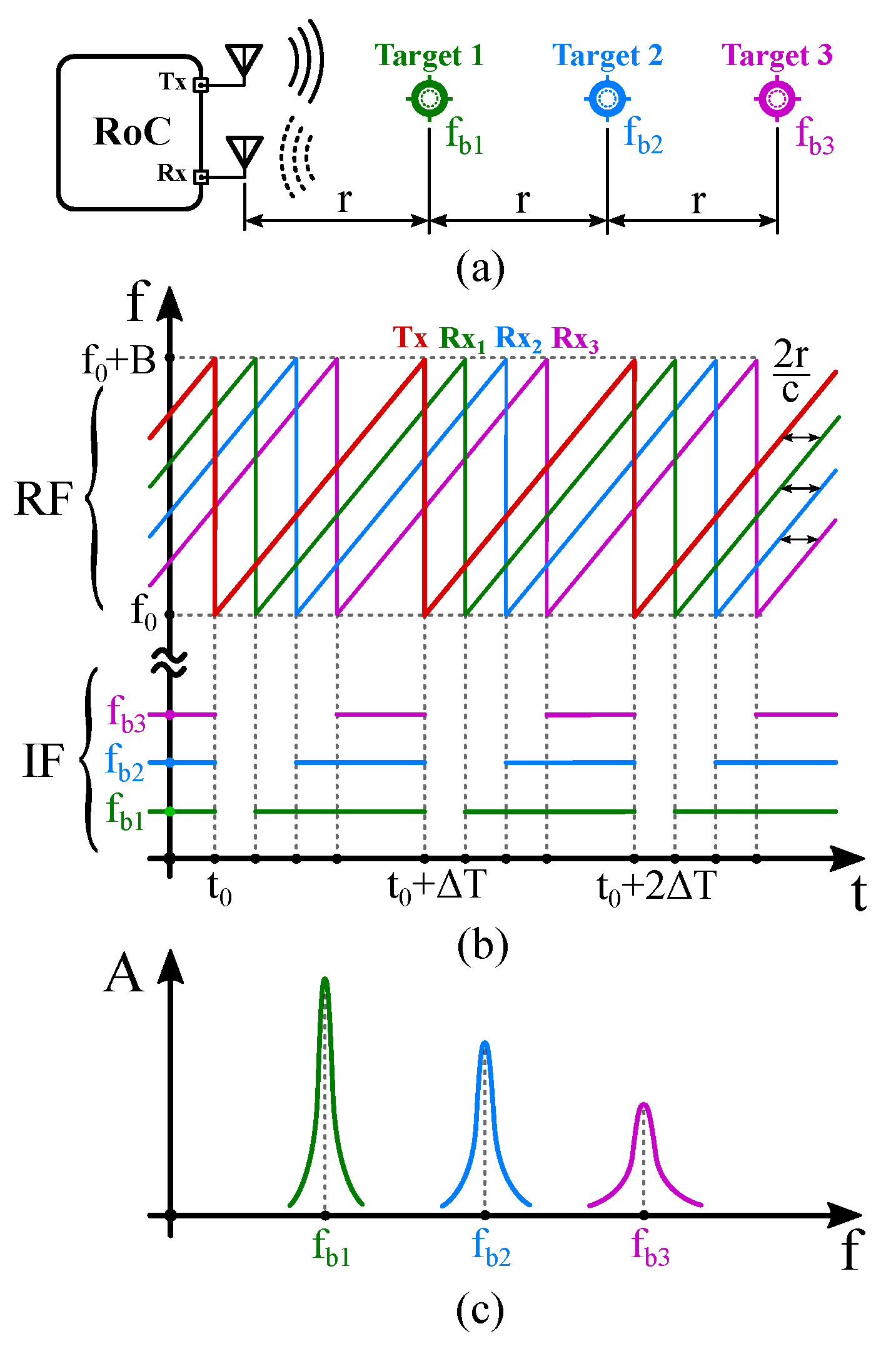
The range processing based on the Fourier transform of the beat frequencies is called “range FFT”. An illustration of the TX and the RX chirps and the beat frequencies extracted by the FFT are shown in
Figure 3.
While range processing is based on the Fourier transform of the beat frequencies, Doppler-induced phase progression over the consecutive chirps (each with a duration of
) is used for velocity estimation. Chirps are commonly designed to be short enough that the distance-induced component of the beat frequency dominates, and their Doppler shift, i.e., the velocity component, is negligible (hence the name fast chirp). The phase progression is given by:
where
presents the round-trip delay change displacement,
is the spatial displacement of an object,
is the wavelength of the transmitted RF signal, and
is frequency of the aforementioned signal. It can be assumed that
. Velocity
v is finally equal to:
Unlike temperature or pressure sensors, where the sensed value is directly correlated with the sensor’s output value, the raw data from the ADC output of the radar front-end (shown in
Figure 2) must be processed before useful information can be obtained. This information can be, but is not limited to, the previously mentioned object range or velocity.
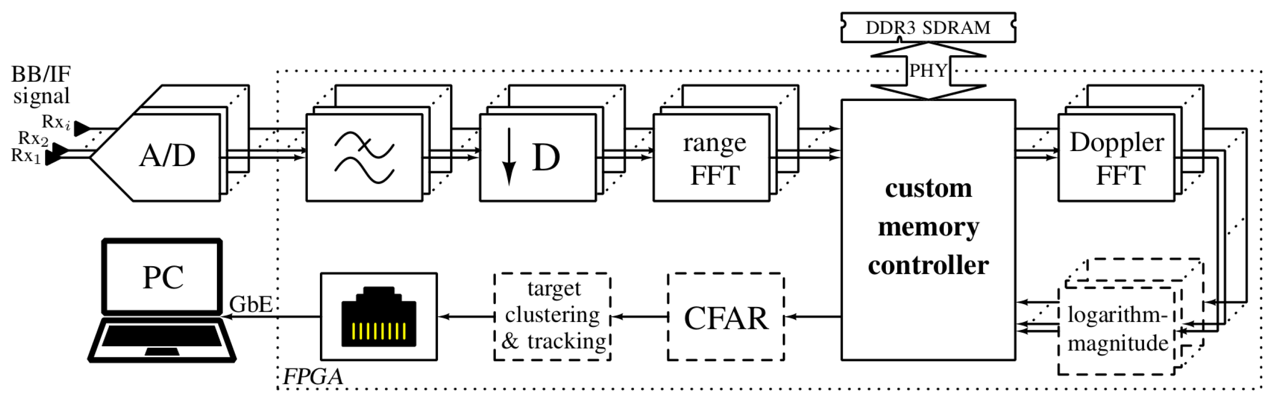
Figure 4 shows a typical radar back-end used for range-Doppler digital signal processing. Usually, data are acquired from an array of ADCs (one ADC per RX channel) and the raw ADC samples are filtered and down-sampled before FFT processing. Multiple parallel processing chains are used to enable real-time data throughput.
In the text to follow, a block of data that contains samples from a single chirp received by the radar back-end and sent by a radar front-end’s ADC will be referred to as a data block.
It is not uncommon for a single vehicle to contain multiple different radar sensors in order to detect objects and obstacles, as well as their location and speed relative to the vehicle. To process the raw data from multiple different radar sensors with a low latency, each radar sensor should have an optimized radar back-end to carry out the processing. In order to accomplish this, the following section proposes a hardware generator for early automotive obstacle detection.
3. Hardware Design Generator Architecture
The proposed open-source hardware generator [
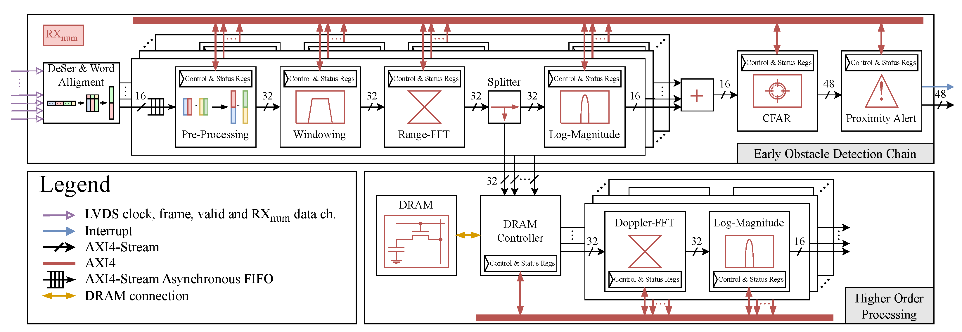
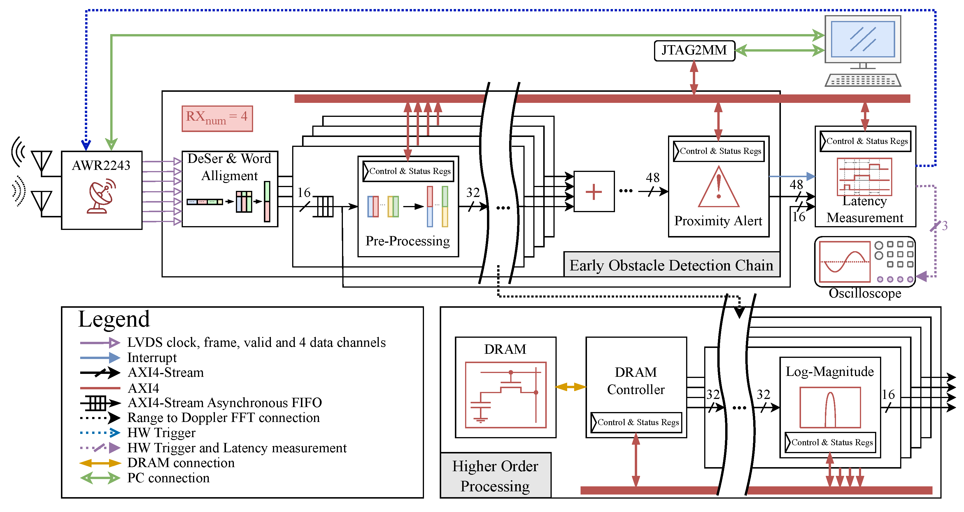
21] was developed with two objectives in mind. The first is that the generator instances should always be prepared to accept new data from the radar front-end. The second objective for the system is to detect obstacles as quickly as possible. For this purpose, the early obstacle detection chain was designed to work concurrently with higher-order processing chain and not to interfere with its operation. A block diagram of the proposed early obstacle detection chain and its connection to the higher-order processing chain (Doppler-FFT and beyond) is shown in
Figure 5.
To achieve full streaming operation for both range and Doppler-FFT, the fully streaming single-path delay feedback (SDF) FFT architecture [
22] was used, which achieves a good balance between resource occupation and execution time [
23]. The remaining components use the input/output AXI4-Stream ready-valid handshake interface and have no effect on the system’s streaming capabilities.
To ensure that both the early obstacle detection chain and the higher-order processing chain operate concurrently, an AXI4-Stream splitter block was used. The splitter block operates as follows: the input data and validity are passed to both splitter outputs, and input ready is only active when both outputs have active ready signals. Because the early obstacle detection chain should not interfere with higher-order processing, the output of the splitter connected to the log-magnitude block must always be ready. To achieve this, all blocks in the early obstacle detection chain following the splitter must be ready at all times. The proximity alert block was designed to accept new data at all times since the log-magnitude and CFAR blocks are both fully streaming.
The proposed generator has a configurable number of RX data channels (RX
num), and all of the blocks shown in
Figure 5 are highly configurable. Compared to an FFT processor for FMCW radar signal processing described in [
9] that includes windowing and magnitude connected in a similar manner as in
Figure 5, the proposed architecture of the FMCW radar baseband processor is much more customizable and thus suitable for interfacing with a much higher number of different radar sensors.
Moreover, latency is a critical factor in the early obstacle detection chain; thus, a method for reducing the system latency was proposed. By flushing data during the time between two consecutive radar data blocks, the system latency can be significantly reduced. The following subsections provide an overview of the used blocks as well as additional information on data flushing.
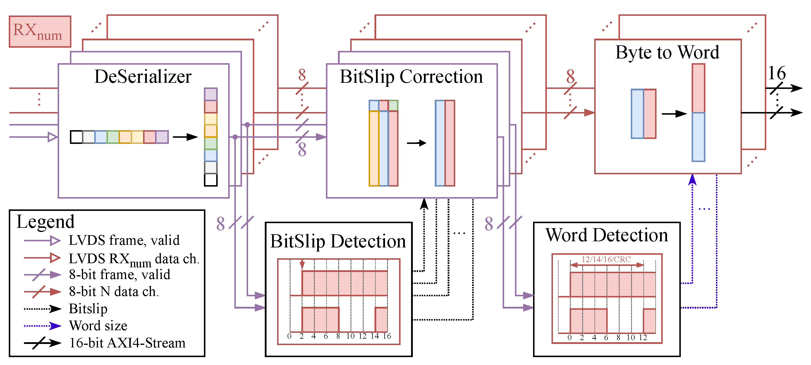
3.1. Deserialization and Word Alignment Block
Radar front-end raw ADC data are typically transmitted over some high-speed serial interface, such as low-voltage differential signaling (LVDS) [
24]. When uncoded data are sent over LVDS lines, additional signal lines are required to aid in timing extraction (for example, frame clock and valid signals). To detect accidental changes in the digital data, some radar front-ends can also send an error-detecting code such as a cyclic redundancy check (CRC).
The deserialization and word alignment block receives data from the radar front-end and converts it to 16-bit words. A block diagram is shown in
Figure 6 and it consists of the deserializer followed by the bitslip detection and correction blocks.
The deserializer module expects DDR (double data rate) data and has a deserialization factor of 1:8. This block needs two different clock inputs to deserialize the input data, a serial radar front-end clock and a clock generated by dividing the serial clock by four (this clock will be referred to simply as the “clock” for the remainder of this subsection and all other blocks in this subsection use this clock).
In order to properly align the received data, the bitslip detection block calculates the bitslip value based on the deserialized frame clock and valid signals (see
Figure 6) and this value is then fed into the bitslip correction block, where the data are aligned.
After detecting and correcting the bitslip value, the word detection block computes the word width using the aligned frame clock and valid signals and can detect word sizes of 12, 14, or 16 bits and a CRC value of 32 bits.
The word size value is then used to perform byte-to-word conversion (12, 14, 16 or 32 for CRC). Missing LSB bits are zero-padded if the word size is less than 16 bits (12 or 14). The byte-to-word block’s output is AXI4-Stream with a data size of 18 bits, 16 bits for the output word and 2 bits for the word size information.
The clock domain crossing from this clock region to the DSP clock region (clock region of the pre-processing block and blocks that follow) is accomplished using AXI4-Stream asynchronous FIFOs. The depth of the used FIFOs is four, and this value has been used for calculation of the worst-case FIFO latency. The block’s overall latency is eight clock periods, four for the deserializer and word detection block and the rest for the asynchronous FIFO.
3.2. Pre-Processing Block
The pre-processing block packs and arranges the received raw ADC data so that the output data stream is adjusted to the subsequent SDF-FFT block. Several radar configuration parameters, stored inside control registers, such as radar data type (complex or real data), flags for sending the first real or imaginary part of the complex data, data block size, number of data blocks inside the frame, etc., are used as control values for the appropriate data packing. This data packing also includes performing zero padding logic to the nearest factor of two when the data block size is not the same as the FFT size.
Additionally, a parallel CRC is calculated on the data block and compared with the received radar front-end CRC in order to detect and potentially prevent issues with LVDS data transfer and, at the same time, false alarms at the output of the chain.
Another important feature of this block is the generation of the last signal (part of the output AXI4 streaming interface) that directly impacts the FFT flushing functionality. The values inside control registers for the data block size and number of data blocks, after which the last signal generated shall be specified.
The overall latency of the pre-processing block is optimized to be only one clock period.
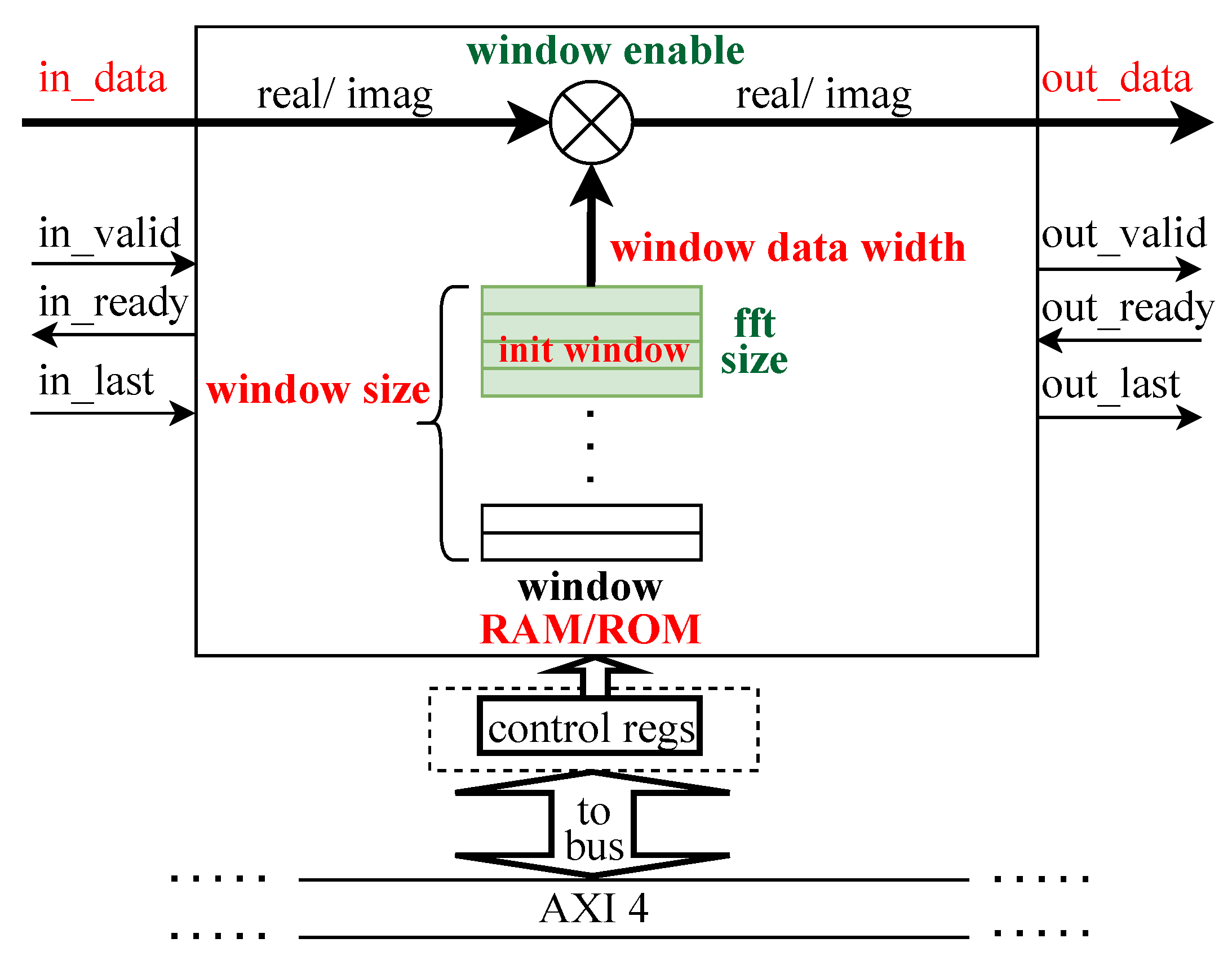
3.3. Windowing
Windowing is used prior to performing an FFT to mitigate the spectral leakage presentable inside the frequency spectrum. A design diagram of the windowing block, showing the input/output signals, the parameters of the module, as well as the control registers, is depicted in
Figure 7. The windowing operation is performed by continuous multiplication of the input samples with windowing coefficients.
The parameter RAM/ROM defines the type of memory where the coefficients are saved. In the case of ROM storage, users can specify one of the following windowing functions: Triangular, Hamming, Hanning, or Blackman. On the other hand, when RAM (BRAM) is selected, any windowing function can be set up by loading memory with coefficients using an AXI4 memory mapped interface during the initialization phase of the system working flow. The init_window parameter determines the initial content of the RAM.
The number of pipeline registers added after the multiplier determines how latency-sensitive this block is. The windowing block has no effect on the system latency if it operates in pass-through mode.
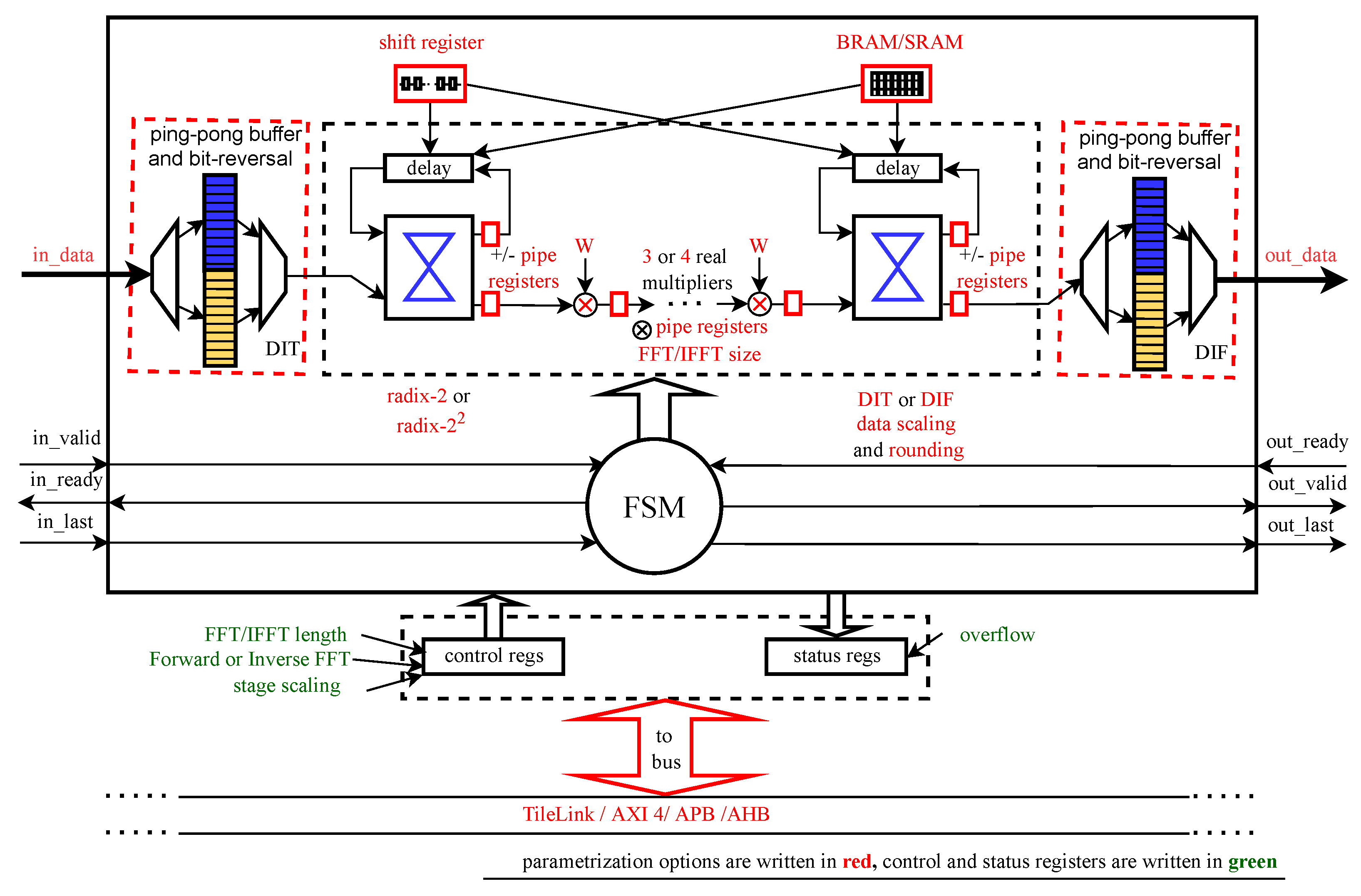
3.4. Single-Path Delay Feedback FFT Processor
Because of its continuous streaming capabilities and as a conceptual compromise between area-efficient memory-based time-multiplexed and direct-mapped fully parallel FFT architectures, the SDF-FFT [
22] was used for both range- and Doppler-FFT. The block diagram of the used SDF-FFT is shown in
Figure 8.
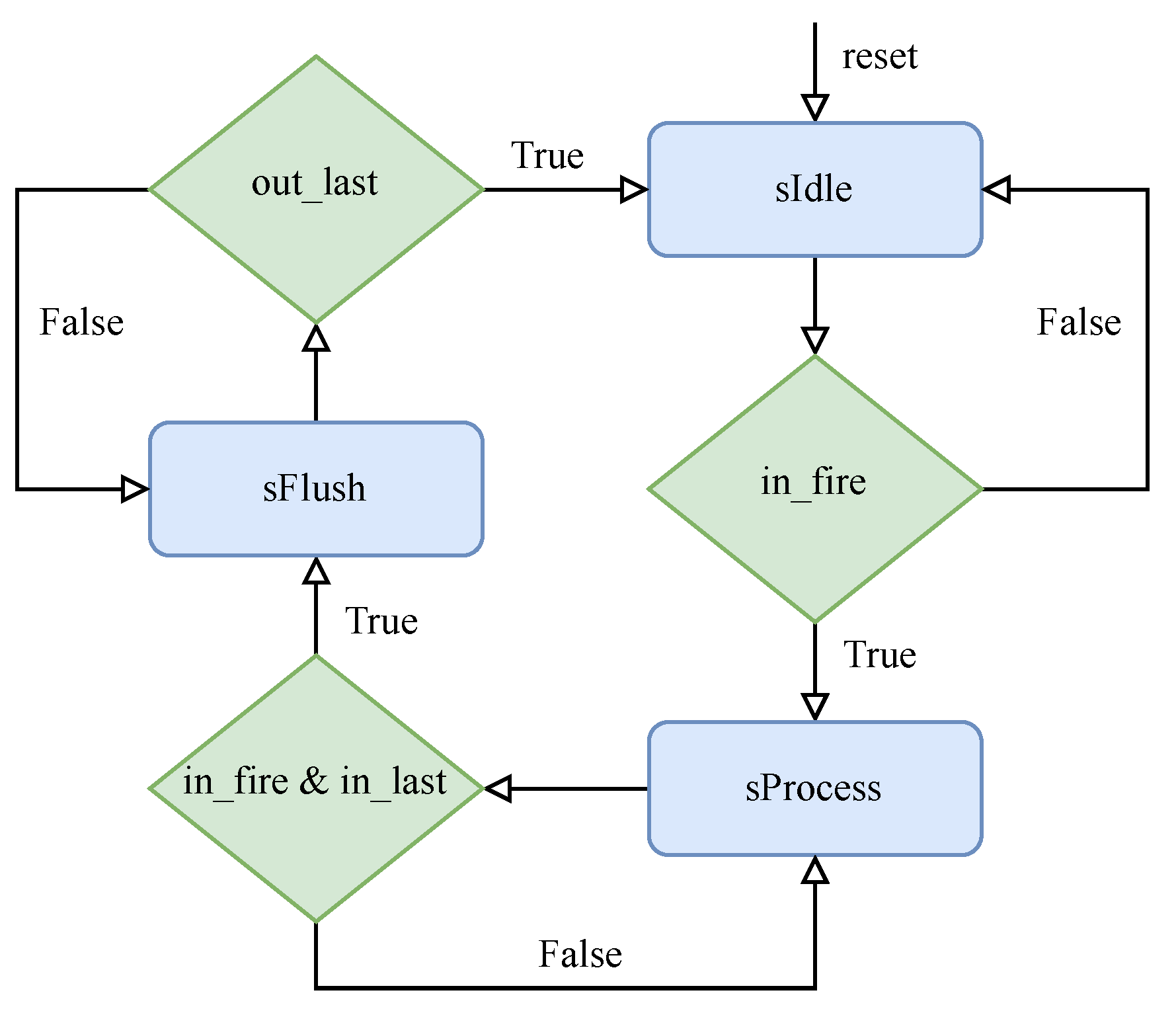
A simple finite state machine (FSM) that controls the data flow of the used SDF-FFT processor is given in
Figure 9. In the FSM diagram, some of the signals are omitted for clarity but a brief explanation of each state is as follows:
sIdle is a reset state and some register initializations are carried out in this state. The system stays in the
sIdle state until the signal
in_fire (in_ready && in_valid) from the input side is not asserted. Data processing is performed in the
sProcess state and when
in_fire is not active, the system stays in this state but the counters predetermined for stage control are frozen. A transition from the
sProcess to the
sFlush state happens if
in_last and
in_fire signals are activated. In the
sFlush state, data flushing is active. Once
out_last (indicating the last sample in the output stream) is asserted, FSM transits to the
sIdle state.
The data flushing feature is essential for reducing the system detection latency. Without the
sFlush state, for the first valid data to appear at the output of the SDF-FFT, two radar data blocks have to be received at the input of the SDF-FFT. However, if the
in_last signal is always generated with the last sample of each data block, the SDF-FFT control logic forces data flushing that can significantly reduce the total latency. During the flushing interval
in_ready is de-asserted, indicating that the SDF-FFT is not ready to accept new radar data until the processing of the current data block is finished. Therefore, to avoid additional delay, the interval between two succeeding data blocks must be longer than the time needed to perform the data flushing operation. A more detailed discussion on this topic is given in
Section 4.
The core latency directly depends on the FFT size, the number of included pipeline registers, the multiplier structure, as well as if the bit-reversal is performed and has the same value for both radix-2 and radix-
scheme and for both decimation-in-time (DIT) and decimation-in-frequency (DIF) butterfly types [
22]. The latency when DIF radix-
scheme is used with four real multipliers and bit-reversal is:
where
is the length of the FFT window and where AddP and MulP represent the number of pipeline registers used for addition and multiplication, respectively.
In the realized design shown in
Section 5 only one pipeline register for both addition and multiplication is used and the size of the FFT is equal to 1024. Based on (
5):
the latency of the used SDF-FFT is 2078 clock cycles.
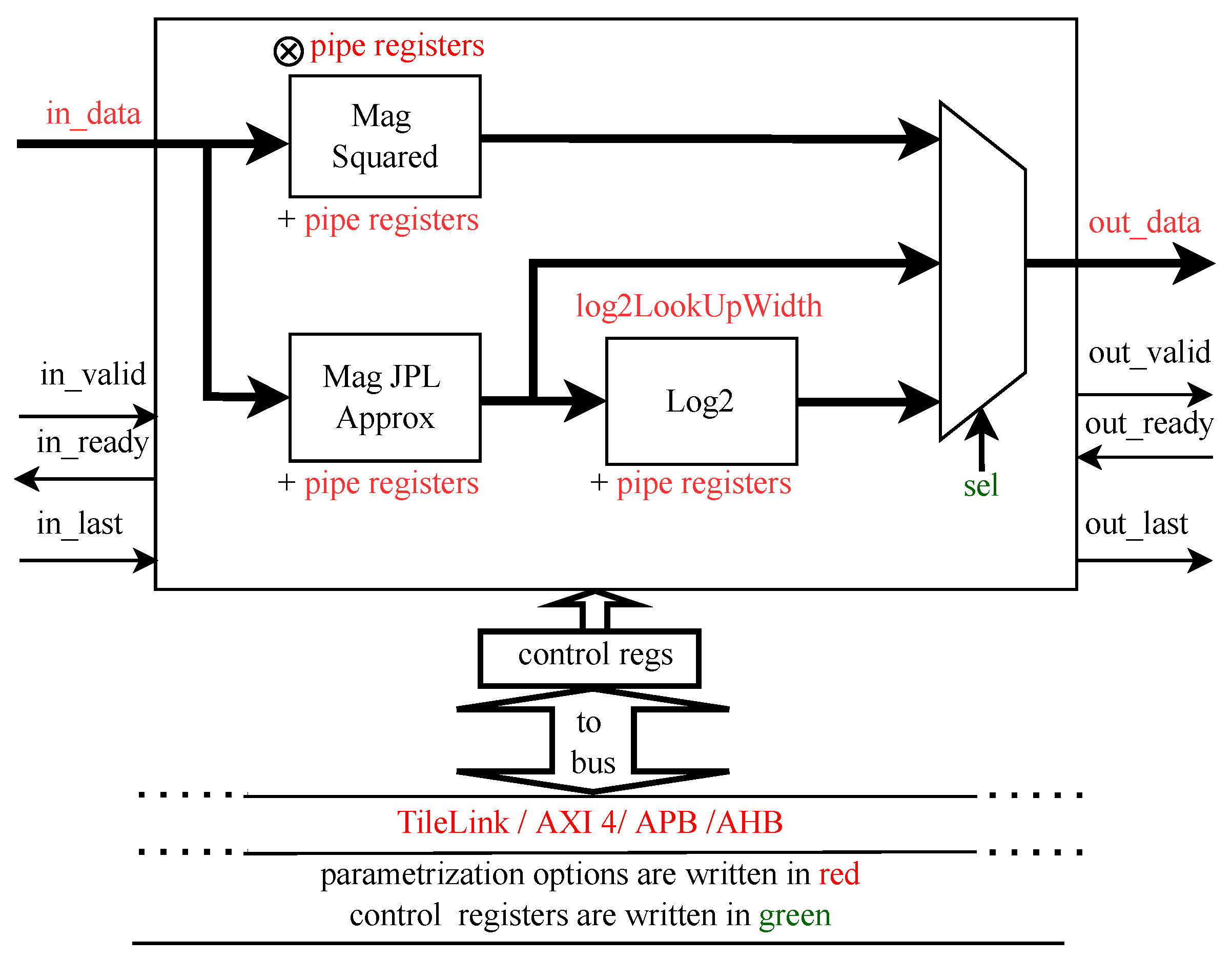
3.5. Logarithm-Magnitude Multiplexer
A fully streaming computation of the input complex sample magnitude, i.e., the absolute value, is performed by the logarithm-magnitude multiplexer (LogMagMux) block, depicted in
Figure 10. Additionally, the squared magnitude and logarithm for the base 2 (
) of the absolute value of a complex input value is also supported.
The computation of the magnitude of the input samples in the magnitude sub-block is realized using the JPL approximation of the square root. Compared to the magnitude approximation used in [
9], the JPL approximation has a significantly lower mean error and standard deviation. The implementation employs only shifters and adders. The estimated magnitude is fed into a log2 computation sub-block that uses a look-up table-based approximation to compute the base-2 logarithm of the magnitude. The squared-magnitude sub-block is the simplest one and employs a few multipliers and adders for its implementation. Each sub-block contains optional pipeline registers for increasing the maximum operating frequency. Those pipeline registers define the latency of the module.
The overall latency of the log-magnitude multiplexer is equal to two times the number of total pipeline registers, which is far less than the complex methods for magnitude and log-magnitude estimation in hardware that employs the iterative CORDIC algorithm. A single instance of this Chisel design generator used in
Section 5 employs three pipeline registers, so the latency is six clock cycles.
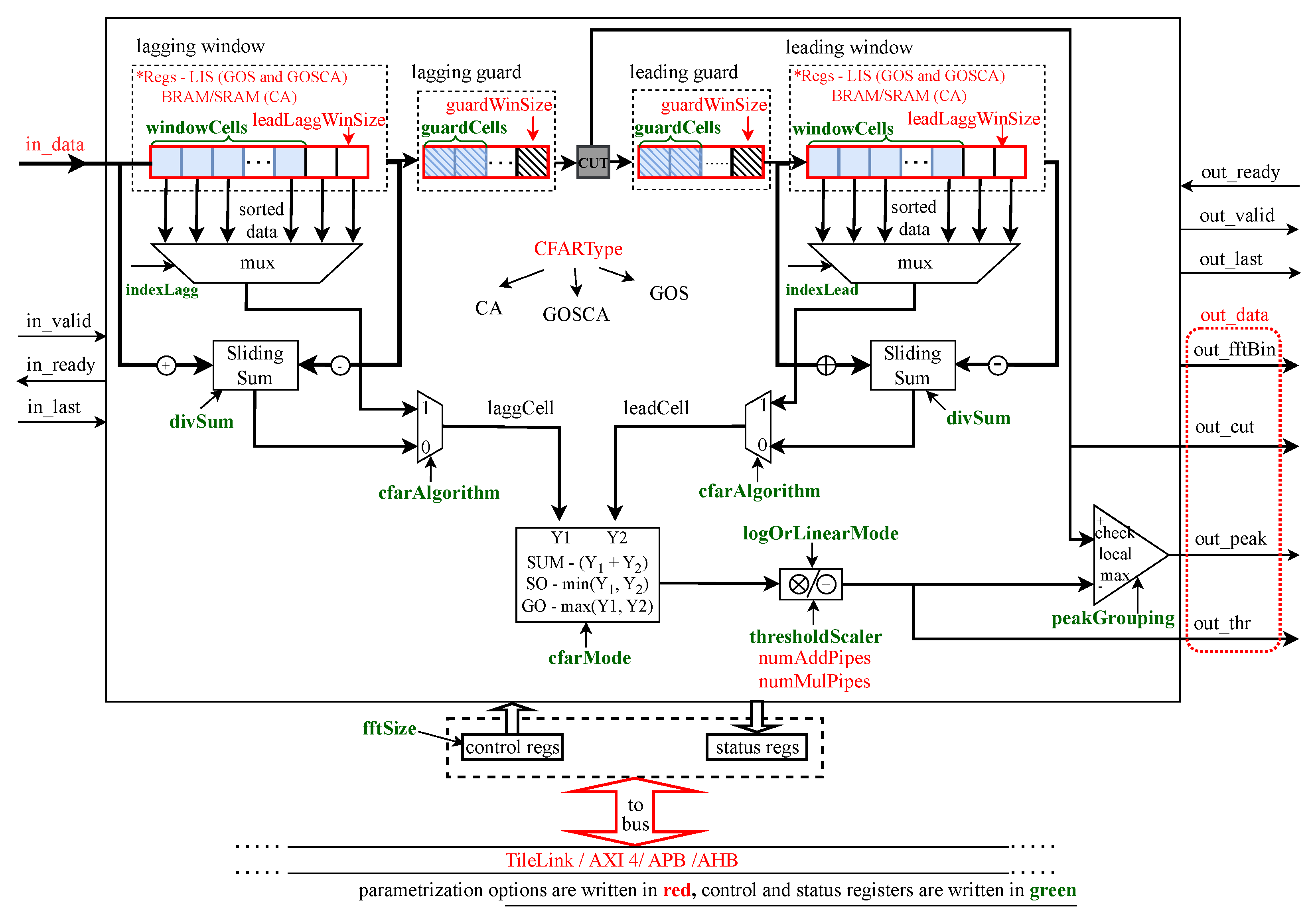
3.6. Constant False Alarm Rate (CFAR) Detector
CFAR detectors are used in radar signal processing systems as an indispensable block for object detection in cluttered and noisy environments. The overall block-level architecture of CFAR detectors, particularly suitable for applications which require continuous data streaming [
25], is given in
Figure 11.
The presented generator of CFAR detectors provides up to six different CFAR algorithms that are available to choose from in compile time and throughout runtime. All these algorithms are implemented such that the input power samples (in_data) are shifted through the lagging and leading reference windows, the guard cells, and the cell under test (CUT); the adaptive threshold is continuously calculated and the CUT value is compared against the obtained threshold to decide whether a peak (object) is detected or not in the present cell. The data sent to the output stream are the current cell under test, threshold, frequency bin inside the FFT window, and single-bit peak signal asserted when an object is detected. The supported CFAR algorithms are divided into two groups based on linear or non-linear operation used for their adaptive threshold calculation.
The first group is linear cell averaging (CA) CFAR algorithms:
Sum CA-CFAR
Greatest of (GO) CA-CFAR
Smallest of (SO) CA-CFAR
The characteristic adder circuit, used for adaptive threshold calculation, is realized using the sliding sum concept where in each clock cycle, the incoming data value is added to the current sum while the leading and lagging window output cells are simultaneously subtracted from it.
The second group of supported CFAR algorithms is the non-linear generalized ordered statistic (GOS) CFAR algorithms listed below:
Cell Averaging (CA) GOS-CFAR
Greatest of (GO) GOS-CFAR
Smallest of (SO) COS-CFAR
Since generalized ordered statistic CFAR algorithms require continuous sorting of the input samples, a FIFO-based linear insertion sorter [
26] is used for the lagging and leading reference window implementation. The architecture of the linear insertion sorter is suitable for real-time data processing. The whole generator can be extended without a lot of effort to support other efficient CFAR algorithms [
27] where bubble sort units can be replaced with high-performance linear insertion sorters, thus saving resources and execution time as well.
In contrast to the FFT, flushing has no effect on the CFAR latency but impacts the CFAR processing time of one FFT data block. The first output data value is generated once the lagging reference window and lagging guard cells are filled with input power samples. In other words, when the last sample of the corresponding data block is received, the number of processed power samples is:
where lag
win is the size of the lagging window, lag
guard is the size of the lagging guard, and the data block size is FFT
size. To process the full data block, additional
data values shall be loaded.
When flushing is inactive, additional
data values are provided by the second input data block. Otherwise, the last signal assertion triggers data flushing, thus ensuring that the rest of the power input samples inside the corresponding data block are processed and the results sent to the output stream. Similarly, as stated in
Section 3.4, during flushing time the CFAR module cannot accept new input data values.
For the CA-CFAR algorithms employed in the design in
Section 5, the overall latency of the CFAR detector is the sum of the lagging window size and lagging guard size. Since the lagging window size was set to 32 and the lagging guard size to 8, the total CFAR latency is equal to 40 clock periods.
3.7. Proximity Alert
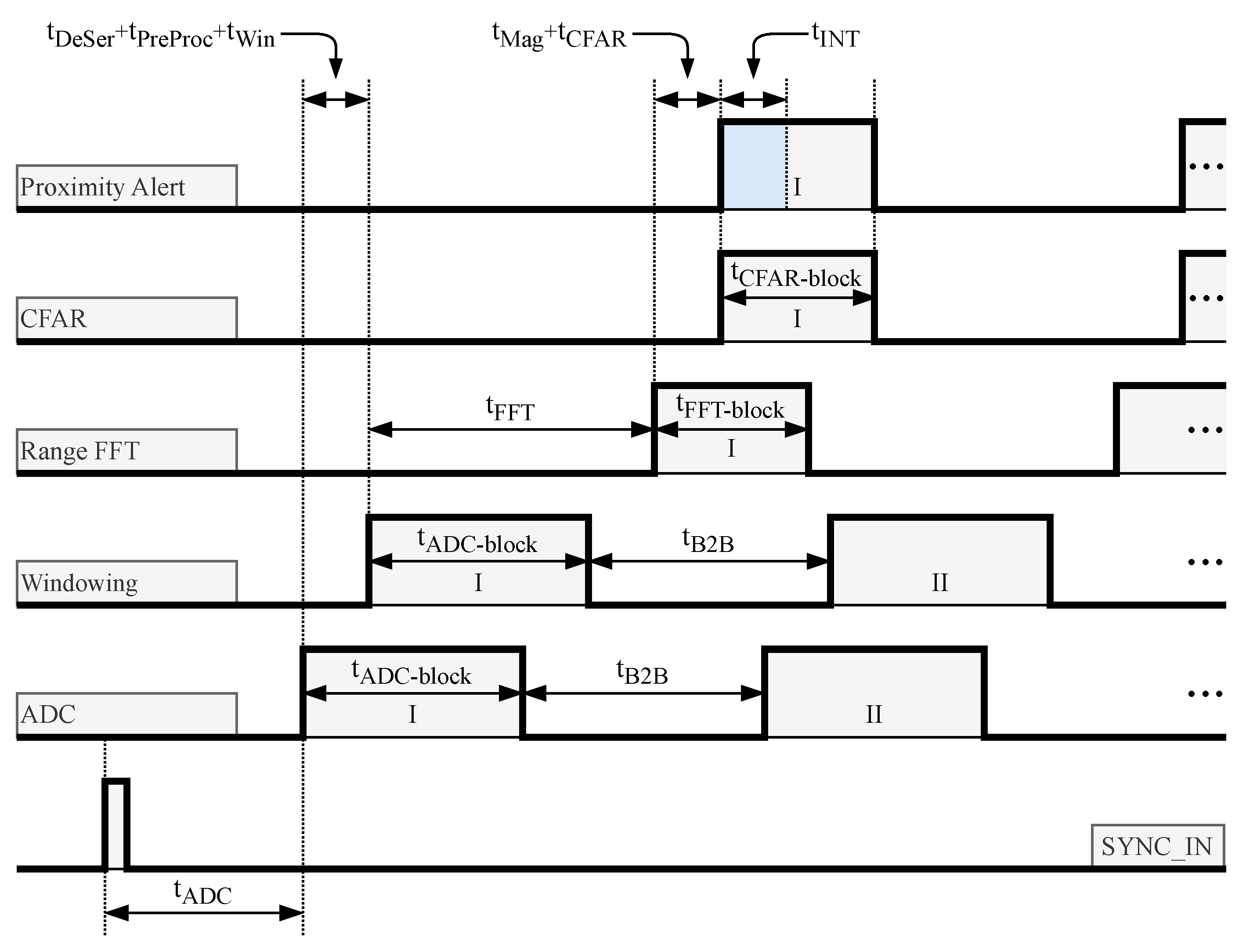
The proximity alert block is used to generate an interrupt when the CFAR detects an object that is closer than the specified range. The range is defined by writing to the corresponding control register. Since the CFAR sends the current bin of the FFT to the proximity alert block, an interrupt will be generated if the CFAR detects an object at the current FFT bin and the bin order is less than the value written in the proximity alert block’s control register. Interrupt generation when the obstacle is too far away can be avoided by writing an appropriate value to this block’s control register.
Figure 12 and
Figure 13 depict the time range t
INT during which an interrupt can be generated. This block has no latency.
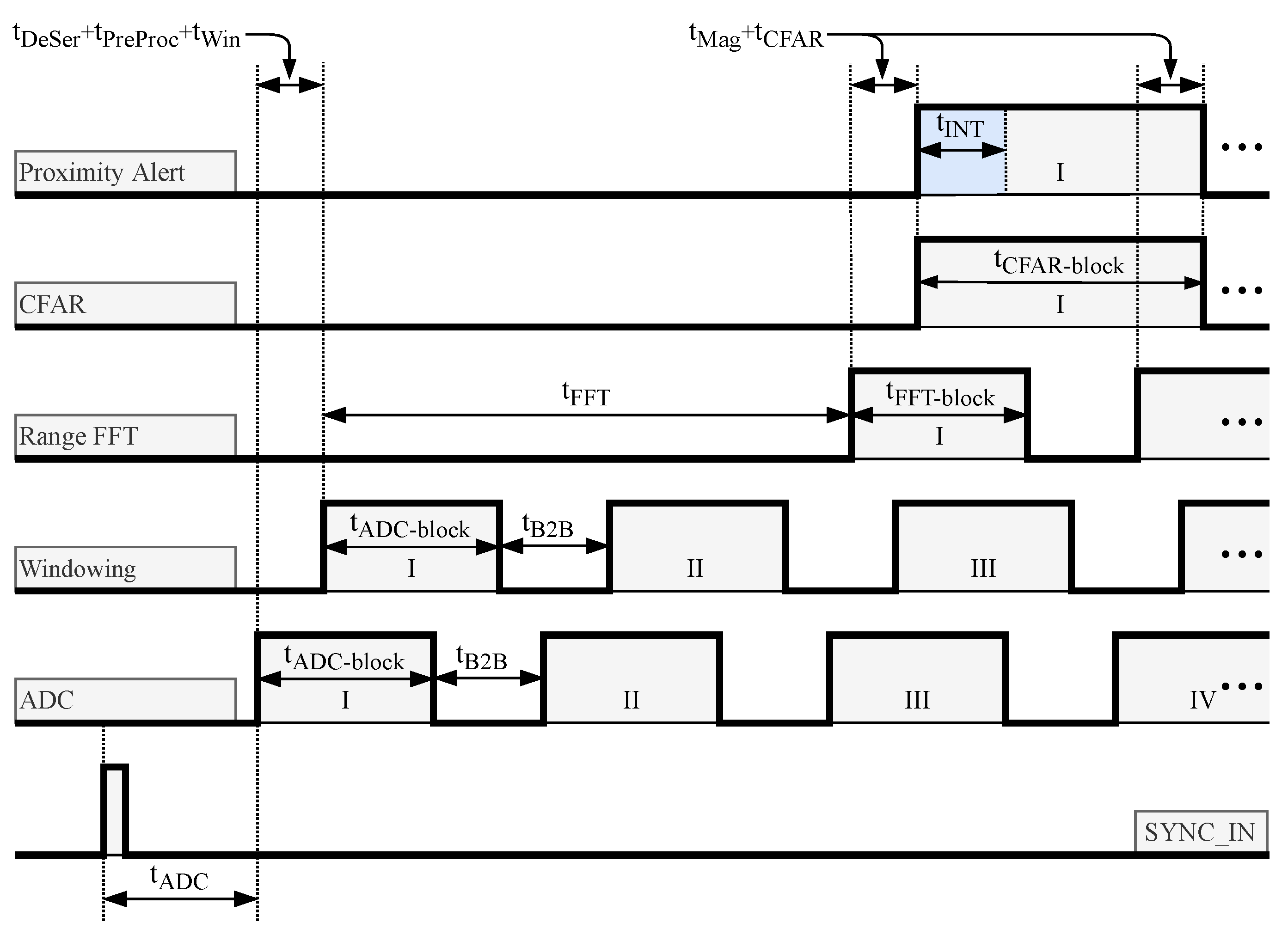
4. System Latency
In order to better understand the limitations and the latency of the system, data diagrams when flushing is inactive are shown in
Figure 12 and when flushing is active in
Figure 13.
To simplify the diagrams, the deserialization and word alignment block, as well as the pre-processing block, were omitted because they are ADC data diagram replicas that have been shifted in time by their respective latencies. The same was carried out for the LogMagMux block, which is the time-shifted replica of the range-FFT data diagram. Considering all the previously calculated latencies for the each block in the early obstacle detection chain, a minimal system latency that depends on both the front-end radar configuration and the proposed system generator parameters is calculated.
The main contributor to the overall system latency is the latency of the SDF-FFT block and to better understand how this latency affects the overall system latency when flushing is inactive,
Figure 12 can be observed. In the first
cycles from (
5) two data blocks are loading into the FFT. After the input data are loaded, additional
cycles are needed to fill the pipeline registers in the SDF-FFT and for the first output data to be generated. The SDF-FFT latency time is equal to:
where
is the duration of a single ADC data block,
is the time between two consecutive ADC data blocks,
is the DSP frequency, and AddP and MulP are the numbers of add and multiplier pipeline registers in the SDF-FFT, respectively.
The time between two ADC data blocks depends only on the radar front-end configuration while the ADC data block duration when data are sent on both edges (DDR) is given by:
where N is the word size in bits,
is both the size of the FFT and the number of samples in a single FMCW chirp, and
is the radar front-end serial frequency.
When flushing is active, SDF-FFT does not need to wait for the second block of input data and instead it generates
zeroes at the input. The SDF-FFT latency when flushing is active is given by:
The second right-hand side term in (
10) represents the time needed to generate
zeroes at the input of the SDF-FFT during flushing. During the time when SDF-FFT fills its input with zeroes no new data should arrive in order for SDF-FFT to function properly and thus the time between data blocks
must be at least the same or larger than the time needed to generate zeroes:
Based on (
8)–(
10), the difference in SDF-FFT latency when flushing is not active and when it is active is equal to:
From (
11) and (
12) for the worst case, when t
B2B is equal to the time needed to generate zeroes, the difference in SDF-FFT latency becomes:
and it can be concluded that the SDF-FFT latency without flushing is always greater than the latency with flushing when condition (
11) is satisfied.
When flushing is active, the FSM state
sFlush from
Figure 9 must be shorter than
from (
11). To avoid dropping input data while in the
sFlush state, the minimum DSP frequency when flushing is active must be at least:
The maximum DSP frequency, on the other hand, is limited by the maximum achievable frequency, which depends on the design implementation. The DRAM controller frequency also limits the DSP frequency. The DSP frequency must be equal to or lower than the DRAM controller frequency in order for the DRAM controller not to drop any data. The maximum DSP frequency can be represented as:
where
is the DRAM controller frequency and
is the maximum achievable frequency for the specific platform.
An important thing to mention is that the flushing functionality is also reducing the time needed for CFAR data block processing (see
Figure 12 and
Figure 13). While the CFAR latency
remains the same with or without flushing, the time needed to process the data block is different due to the way the CFAR lagging window and guard are filled. As mentioned in
Section 3.6, to process the full data block when flushing is inactive additional data must be read from the second input block by CFAR equal to the sum of the lagging window and lagging guard size (
Figure 12). The CFAR processing time when flushing is inactive is equal:
When flushing is active, after the
in_last from
Figure 11, CFAR will generate additional zeroes to fill the lagging window and lagging guard, so the processing time is equal to the FFT processing time:
If the condition from (
11) is met, the CFAR block processing time with flushing is shorter than the CFAR processing time without flushing.
Based on the previous equations and from the block latencies given in the previous chapter, it can be calculated that the overall early obstacle detection chain latency,
, equals:
where
is the deserialization and word alignment block latency,
is the pre-processing block latency,
is the windowing block latency,
is the LogMagMux block latency, and
is the CFAR detector block latency. These latencies are equal to the latency (in clock cycles) of the block divided by the clock frequency. The
is the FFT processor latency given by (
8) when flushing is inactive and by (
10) when flushing is active.
For the Artix-7 FPGA used in
Section 5, the maximum DDR data frequency [
28] is 200 MHz and the maximum logic frequency without time violations is slightly higher than 200 MHz. Based on (
15), the maximum DSP frequency for the setup given in
Section 5 is equal to 200 MHz.
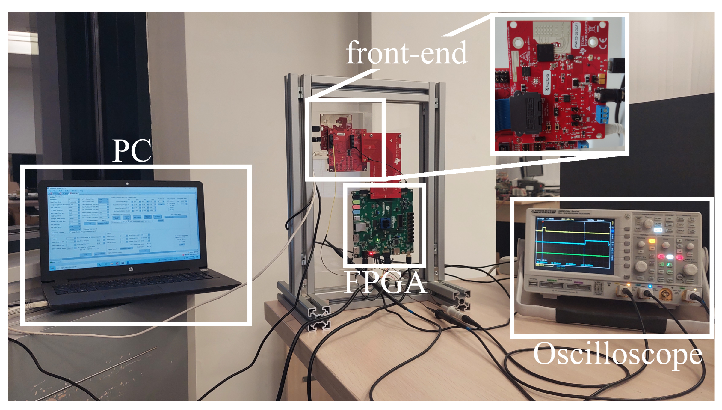
5. Experimental Results
Commercial off-the-shelf (COTS) modules were used for all of the experiment setup apparatus. A single instance of the proposed generator was synthesized and implemented on a Digilent Nexys Video board based on Artix-7 FPGA from Xilinx. Texas Instruments AWR2243 was used as a radar front-end. The connection from the AWR2243 evaluation module [
29] to the FPGA board was realized over an FMC connector [
30]. In order to emulate the real case use of the proposed early detection chain, a higher-order processing chain consisting of Doppler FFT, magnitude block, and DRAM controller was also implemented. To create the experimental setup, the architecture from
Figure 5 was supplemented with the latency measurement block in order to perform latency measurements. The experimental setup block diagram is given in
Figure 14, while the physical setup is shown in
Figure 15. An overview of the key generator parameters and the AWR2243 FMCW chirp parameters are given in
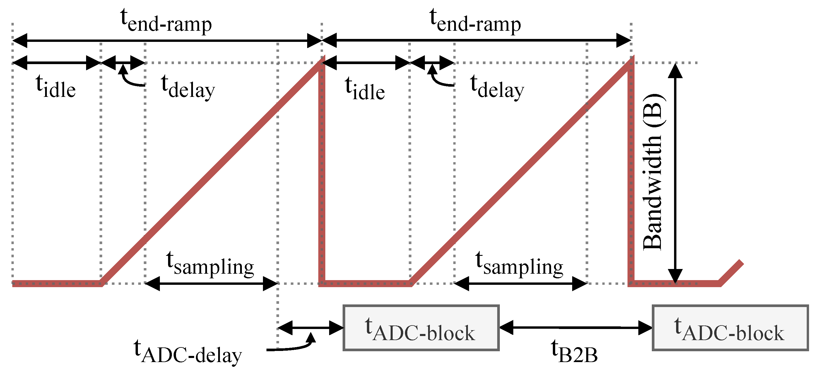
Table 1. A time diagram of the typical FMCW chirp is presented in
Figure 16.
Based on the FMCW chirp parameter values given in
Table 1, the sampling time interval from
Figure 16 is equal to:
From (
9) ADC data block duration
can be calculated and it is equal to 36.4 µs. From
Figure 16, the time between two consecutive ADC data blocks is:
Based on (
14), the minimum frequency for the early obstacle detection chain is equal to approximately 31.9 MHz. On the other hand, the maximum frequency for FPGA given by (
15) is equal to 200 MHz due to the DRAM frequency limitation. The DSP frequency was set to 200 MHz.
The AWR2243 device supports a hardware-based mechanism to trigger radar frames. An external host can pulse the
SYNC_IN signal to start radar frames [
24,
29]. The latency measurement block in
Figure 14 acts as an external host to the AWR2243. The second functionality of the latency measurement block is to calculate the overall system latency. This block consists of a simple FSM that asserts the
SYNC_IN signal so that the AWR2243 can start sending frames. The latency measurement block generates three output signals that are observed on the oscilloscope:
SYNC_IN and two signals used for latency measurement (
S_IN and
S_OUT).
After the user has written in the appropriate control register of the latency measurement block, FSM begins to execute. The signal
SYNC_IN is then generated, and the duration of the
SYNC_IN is set by writing the duration value into the appropriate control register of the block. From the AWR2243 documentation, this duration must be at least 25 ns [
24].
The output signal of the latency measurement block S_IN is asserted when the first data arrive at the pre-processing block’s input. When the last data at the input arrive, this output will be de-asserted. The data block size should be pre-written to the latency measurement block’s control register in order for the FSM to correctly de-assert the S_IN signal. In other words, the duration of the single data block at the pre-processing block’s input is represented by this S_IN output signal. In order to avoid complicated clock crossing from the deserialization and word alignment block to the latency measurement block, only the data block duration at the input of the pre-processing block is measured. The deserialization and word alignment block latency is equal to 0.07 µs (8 clock cycles with the clock frequency of 112.5 MHz, which is the AWR2243 serial frequency divided by 4) and this time is negligible compared to other values.
The output S_OUT is generated in the same manner as the S_IN, but for the proximity alert block output. In other words, the duration of the data block at the end of the early obstacle detection chain is represented by the S_OUT signal.
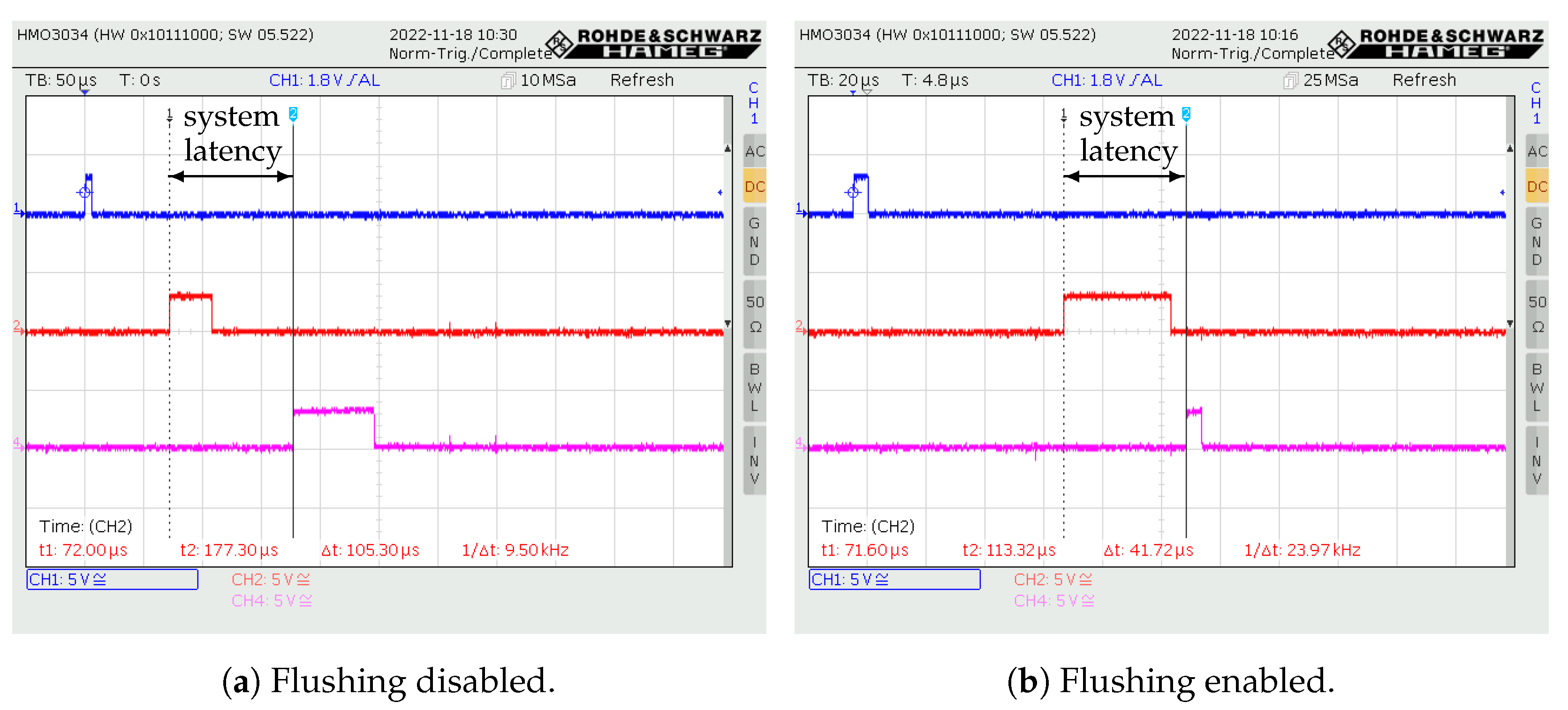
The time elapsed between the positive edge of the signal SYNC_IN and the positive edge of S_IN is equal to the time required for the first data to arrive at the pre-processing block input from the radar front-end after the hardware trigger was asserted.
The time between the positive edge of the signal
S_IN to the negative edge of the same signal is equal to the data block duration
at the input of the pre-processing block. The expected duration of the
is given by (
9). The measured values are shown in
Figure 17a,b when flushing is inactive and when it is active, respectively.
The time between the positive edge of the signal
S_IN and the positive edge of the signal
S_OUT is equal to the latency from the pre-processing block to the output of the system. To obtain the overall system latency, the deserialization and word alignment block latency should be added to the previously mentioned value. This measurement can be used to approximate the overall system latency since the deserialization and word alignment block latency is negligible. This measurement is shown in
Figure 18a,b when flushing is inactive and when flushing is active, respectively. When flushing is inactive the overall latency time can be calculated using (
8) and (
18). For the case when flushing is active, the overall latency time can be calculated using (
10) and (
18).
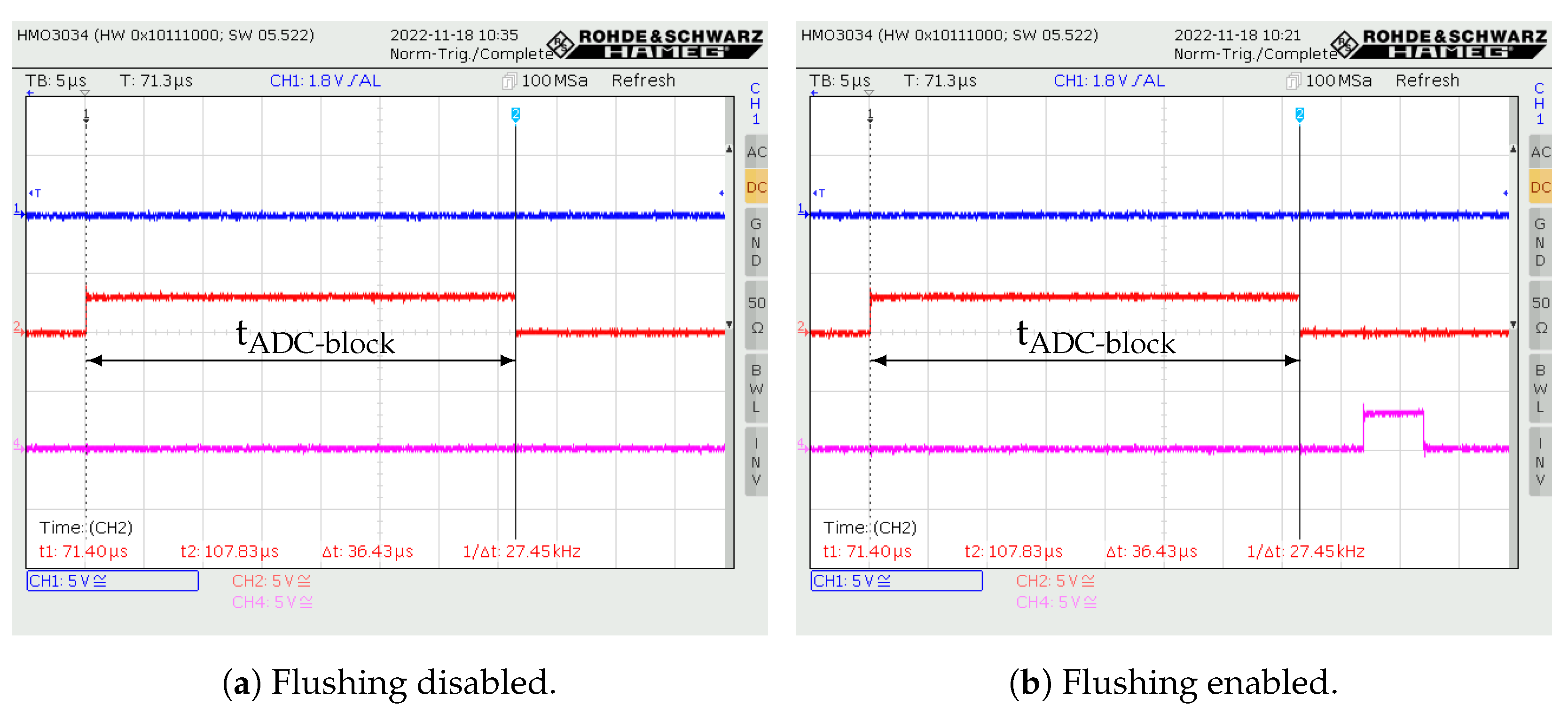
The single CFAR data block processing time
(proximity alert block has no latency) can be calculated by measuring the time between the positive edge of the signal
S_OUT and the negative edge of the same signal. The CFAR block processing time is shown if
Figure 19a when flushing is inactive and in
Figure 19b when flushing is active. When flushing is inactive the duration of the
is given by (
16) and when flushing is active it can be calculated using (
17).
An overview of the measured signals when flushing is inactive and when it is active is given in
Table 2. The calculated values are shown in
Table 3. The value from the positive edge of the
SYNC_IN signal to the positive edge of the
S_IN signal is not calculated since this value depends only on the radar front-end used. Comparing the calculated and measured values from
Table 2 and
Table 3 while keeping in mind that the measurement step of the oscilloscope was between 0.1 µs and 0.4 µs depending on the oscilloscope configuration, it can be seen that the measured values confirm the presented calculations.
By utilizing the flush capability of the proposed generator, for this example, the latency of the system was reduced by about 60.38%. The FPGA resource utilization is given in
Table 4. The resource utilization shows that the proposed design can be implemented on a relatively inexpensive and commercially available FPGA board.
6. Conclusions
This manuscript presented an open-source hardware architecture for the early detection of automotive obstacles that does not impede the operation of the higher-order processing. A method for reducing the overall system latency was proposed and the minimal achievable latency constraints were given. The architecture was developed as a highly parametrized hardware generator that is suitable for interfacing with different types of automotive radar front-ends. For one such radar front-end, TI AWR2243, a single instance of the proposed generator was synthesized and implemented on Digilent’s Nexys Video board based on Artix-7 FPGA from Xilinx. The measured latency of the early detection chain without the proposed method was 105.3 µs, and when the proposed method was used it was 41.72 µs; thus, by using this method the overall system latency was reduced by approximately 60.38%.
It is not uncommon in modern autonomous vehicles to process radar data using a higher-order radar signal processing method, such as Doppler FFT, and then feed the processed data into a large deep learning neural network that determines what is ahead of the vehicle and whether to brake or accelerate. The Doppler processing time can range from milliseconds to tens of milliseconds depending on how the radar front-end is configured, whereas the neural network inference latency is typically much longer, ranging from tens to hundreds of milliseconds. During this time, the vehicle can travel a few meters on the highway. By utilizing the proposed method for time-critical applications, which has a significantly lower latency (bellow 100 µs), braking can occur a few meters earlier, potentially preventing accidents.


