Abstract
In this paper, a parasitic-design-aware simulation-based design tool is proposed for highly linear RF power amplifiers. The main aim of the proposed tool is to speed up the design process of RF power amplifiers. In addition, it provides accurate final designs taking into consideration the effect of parasitic components of both active and passive devices. The proposed tool relies on the knowledge of designing highly linear RF power amplifiers. Both the optimization steps and design methodology are presented in this paper. The proposed tool is verified by designing a highly linear RF power amplifier at three different frequencies (7 GHz, 10 GHz, and 13 GHz) using 65 nm technology node. The results show that an OP1 dB higher than 18 dBm, gain/S21 higher than 7 dB, and OIP3 higher than 24 dBm at 6 dB back-off power can be obtained.
1. Introduction
Today, for any wireless transceiver, the RF power amplifier (PA) is considered one of the important building blocks. This is because RF power amplifiers determine the maximum transmitted power. Designing CMOS RF power amplifiers is challenging due to several factors: First, the different performance specifications of a power amplifier, such as Gain, output 1 dB compression point (OP1 dB), efficiency, and output linearity are dependable on each other. Second, those performance specifications are limited by the existing layout parasitic components of both active and passive devices. Finally, it takes several, time consuming design iterations to account for the electromagnetic interaction between the various passive components within the design [1,2,3,4,5,6,7,8].
Design automation could help to reduce this design time and to reach an optimum design that meets the design targets [9,10]. However, the aforementioned challenges present a limitation even if design automation is used. Design automation approaches that overcome these challenges (trade-offs, effect of parasitic components, and electromagnetic interactions), while reducing time consuming electromagnetic (EM) simulations and layout parasitic extraction, are required.
The design automation of RF circuits, applied for the optimization of a low noise amplifier (LNA), was introduced in [11] where a Pareto-optimal front (POF) of EM-simulated inductors was obtained prior to the optimization. This approach is an offline design methodology where the inductor pareto-optimal fronts are independent of the circuit. Another design automation approach, used for the optimization of a folded cascode operational transconductance amplifier (OTA), was presented in [12], where a simulation-based circuit sizing tool with a template-based layout generation tool were shown. The simulated-annealing-based optimization of a class C CMOS RF power amplifier (operating at a frequency of 900 MHz) was introduced in [13]. The effect of the inductors was taken in consideration by introducing a compact model including some of the parasitic components of the inductor. However, simulated-annealing optimization has slow convergence rates. A simulation-based optimization of RF amplifiers (operating at frequencies less than 10 GHz) was presented in [14], where an online inductor surrogate model was built using machine learning techniques. The main challenge of this approach was that the quality of the surrogate model is not always good, and it depends on the available training data. Evolutionary algorithms were used in the optimization of an LNA in [15], but no inductance modelling was included. Metaheuristics were used in the optimization of an LC voltage-controlled oscillator (VCO) and a CMOS current feedback operational amplifier (operating at a frequency of 1.5–2.5 GHz), using 2п inductance modelling [16]. Evolutionary algorithms were also used in the optimization of an operational amplifier (OPAMP) and an LNA, where the inductance modelling was carried out using linear behavior into performance models [17]. Evolutionary algorithms and simulated-annealing were used in the optimization of single ended LNA and CMOS differential cross coupled oscillator operating at 2.4 GHz frequency [18].
In this paper, a simulation based, design-aware, parasitic-aware optimization tool is introduced for the design of highly linear RF CMOS power amplifiers. The introduced tool overcomes the previously mentioned design challenges by integrating the design experience within the optimization loop to speed up the design process. This design experience has to be programmed once and can be used later for all other designs at different frequencies and using different technology nodes. In addition, parasitic components are estimated such that the outcome of the design tool is close to the final design. The proposed design-aware tool does not require the design space exploration and/or the lengthy global optimization algorithms that were presented in the previous publications [11,14,15,16,17,18]. The tool uses BFGS optimization algorithm, implemented within the virtuoso environment [19], as the core optimizer, and Spectre RF [20] as the simulation engine. The paper is organized as follows: An overview of the proposed design tool and an illustration of the PA architecture adopted in the tool are introduced in Section 2. Section 3 discusses the parasitic modelling approach adapted within the tool. In Section 4, the details of the design-aware optimization and the design flow are explained where the knowledge of the designer is integrated within the tool. Test cases and the results of the optimization are shown in Section 5. A discussion is found in Section 6. Finally, the paper is concluded in Section 7.
2. The Proposed Design Tool for RF Power Amplifiers
The core of the introduced design tool is made up of four main parts; the web interface, the CAD RF circuit simulator, the Parasitic Model Generator, and the Optimizer. Figure 1 shows a simplified diagram of the core of the introduced design tool. The user enters the required performance specifications of the RF power amplifier to the web interface. The web interface is developed using PHP, HTML, CSS, and Java scripting. The communication between the web interface and the RF circuit simulator (cadence-virtuoso) is established through shell scripting and ocean scripting. The CAD RF Circuit Simulator (cadence-virtuoso) is updated by the required performance specifications from the web interface. Then, it invokes the cadence built-in optimizer, which updates the netlist of the adopted highly linear RF power amplifier schematic. Multi-objective optimization is carried out by the hybridization of design-aware optimization flow and the BFGS optimization algorithm [21,22], which is employed in cadence built-in optimizer. The BFGS algorithm is used for finding the best values of the design parameters that can meet the required constraints. The parasitic models are priorly constructed within the parasitic model generator and their values are updated by the optimizer. The new values are included in the updated netlist. The optimization process continues till reaching the best achieved design point. The resulting design parameters are then returned to the user along with the achieved performance. The highly linear PA architecture, adopted as an application for the proposed tool, is explained below.
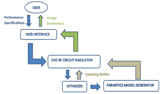
Figure 1.
The core of the design tool.
The Adopted Highly Linear PA Architecture
Figure 2a shows the highly linear power efficient RF CMOS power amplifier architecture adopted by the introduced tool. The architecture is based on achieving high linearity by using parallel cascoded configuration (PCC) topology introduced in [23]. Figure 2b shows the PCC amplifier topology that improves the linearity of RF power amplifiers through transconductance linearization. The topology is made up of two parallel-connected cascode branches. The common source (CS) amplifier, used in the main branch, is biased to operate as a class-AB power amplifier carrying most of the consumed current. while the auxiliary amplifier is biased to operate as a class B amplifier. Transconductance linearization is achieved by choosing the biasing voltages and sizes of the main and auxiliary common source amplifiers such that the non-linearities of both branches are partially cancelled out when added together. If the biasing and sizing of both branches are chosen such that the nth-order transconductances of the main and auxiliary amplifiers, Gn_main and Gn_auxiliary, have almost similar magnitudes and 180 degrees phase shift, their summation at the output node results in their partial cancellation.
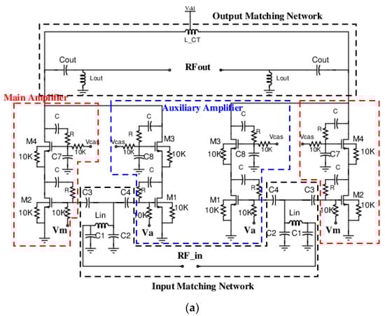
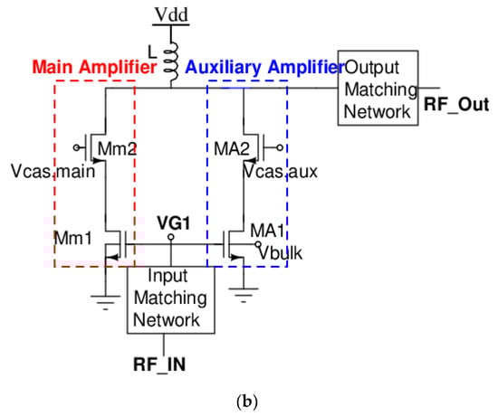
Figure 2.
(a) Highly linear RF power, (b) the idea of the adopted topology.
Based on (1), (2), and (3), the partial cancellation of transconductance non-linearities results in the cancellation of third-order and fifth-order intermodulation distortion (IMD3 and IMD5) as well as the cancellation of third order harmonic distortion (HD3) [23].
where iDS_3, iDS_5 and iDS_3fo are the third, fifth-order intermodulation components (IMD3 and IMD5) of drain current, iDS, and third-order harmonic distortion (HD3), respectively. The cancellation of non-linearities at back-off power results in better linearity and higher efficiency.
As shown in Figure 2a, the main and auxiliary common source devices have separate DC gate biasing. This gives an extra degree of freedom in having different combinations of biasing voltages and sizes of both branches to achieve the required linearization. The input matching network used has a slight modification from the commonly used pi-matching network, where C3 and C4 are added to be part of the input matching network to allow both branches to have a single input matching network. The Cascoded configuration is used to overcome breakdown voltage limitations of CMOS devices. The differential configuration reduces the bond-wire effect of source grounding [23] and even-order intermodulation distortion components (e.g., IMD2 and IMD4). Stability is maintained in the circuit by using negative feedback loops made up of series RC networks. These negative feedback loop components are optimized to maintain stability without causing a severe gain decrease. C7 and C8 are placed at the gates of the cascode devices of both the main and auxiliary amplifiers and optimized to maintain equal VDS swings across the common source and the common gate devices of each branch despite any change in input power. The output matching networks are pi-matching networks where a center-tapped inductance is used as shown in Figure 2a.
3. Parasitic Modelling
Including the layout parasitic components in the design process saves a lot of time and effort. It results in accurate designs whose performance specifications are the same before and after post layout simulations.
3.1. Parasitic Modelling for Passive Devices
The inductances and capacitances used in the optimization process are the foundry process design kit (PDK) devices, their corresponding parasitic components are included within the design kit models. The optimization of the physical parameters of passive devices is carried out. The physical parameters of the inductance that are to be optimized are the inner radius and the number of turns, while those of the capacitance are the length and width.
3.2. Parasitic Modelling for Active Devices
The modelling of the parasitic capacitances arising from transistor layout and its interconnects when operating at gigahertz frequencies is carried out and included in the schematic to be taken in consideration during optimization.
Figure 3 shows the parasitic-aware MOSFET model used within the proposed tool. Using S-parameter simulations of the parasitic extracted view of the PDK transistor taking in consideration parasitic components arising from its interconnects, the impedance values seen from its three terminals are plotted with respect to frequency. Thus, the excess capacitances of Cgs, Cgd, and Cds resulting from the layout are estimated. These values are calculated at different values of channel width. Figure 4 shows the excess capacitances of Cgs, Cgd, and Cds versus the width of the transistor. As depicted, as the width of the transistor increases, those capacitances increase linearly. Polynomial expressions of the parasitic capacitances as functions of the number of fingers of the transistor are obtained using least-mean squares curve-fitting method. Equations (4)–(6) show the resulting expressions of the parasitic capacitances after taking the number of multipliers (M) of transistor in consideration.
where N is the number of fingers and M is the number of multipliers of transistors. The finger width is fixed to 2 µm.
Cgs (in fF) = (1.1 N + 1.5) ∗ M
Cgd (in fF) = (1.1 N + 0.4) ∗ M
Cds (in fF) = (1.59 N + 1.69) ∗ M
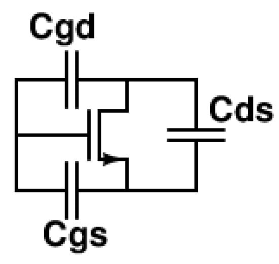
Figure 3.
Parasitic-aware transistor model.
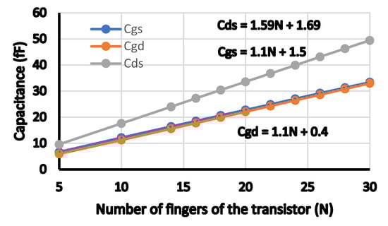
Figure 4.
Cgs, Cgd, and Cds versus the number of fingers of RF transistor (N).
4. Design- Aware Optimization and the Proposed Design Flow
4.1. Design Trade-Offs and Sensitivity Analysis
The key component of the proposed design-aware optimization is to combine the knowledge of the designer along with the optimization. For the power amplifier shown in Figure 2a, almost all the design parameters are affecting all the performance specifications. Those specifications include the output 1 dB compression point (OP1 dB), Gain, output third order intercept point (OIP3) at the operating power, power added efficiency (PAE), and input/output matching. The sensitivity of each performance specification to each design parameter (width, biasing, capacitances, and inductances) is different. For the proposed design-aware optimization, those sensitivities are identified and taken in consideration to speed up the design time. Trade-offs are also understood from this sensitivity test.
Below, some examples showing the sensitivity of the performance specifications to the various design parameters are discussed and verified with simulations. Table 1 lists typical values of the design parameters that are used for the sensitivity analysis/simulation. Figure 5a shows the simulation results of the OIP3 versus the output power for different channel widths of the transistors of the main and auxiliary amplifiers. As depicted, the OIP3 depends significantly on the width of the channel of both the main and auxiliary branches. This is because the OIP3 relies on the non-linearities cancellation between these two branches.

Table 1.
Values of all the design parameters in Figure 2a.
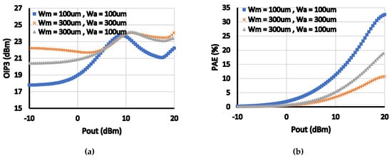
Figure 5.
(a) OIP3 versus Pout, (b) power added efficiency (PAE) versus Pout for different sizes of main and auxiliary amplifiers.
It is important to note that the highest OIP3 values are achieved when both sizes are equal to 300 µm, yet the corresponding PAE is the worst as shown in Figure 5b. The best efficiency is achieved when both transistors have sizes equal to 100 µm, while the OIP3 shows a peaking around 10 dBm. The dependency of OP1 dB on the width of the channel is shown in Figure 6, and as expected the larger the width, the higher the achieved OP1 dB. Those simulations indicate that the channel width of both the main and auxiliary branches determine the OIP3, OP1 dB, and efficiency. There is also a tradeoff between those performance parameters (efficiency and OP1 dB/OIP3). Thus, reaching the required design targets could be time consuming task.
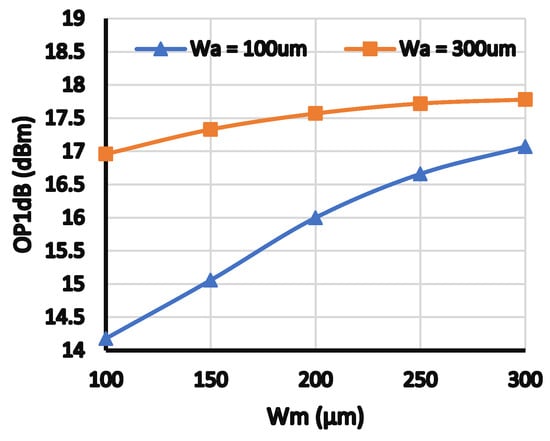
Figure 6.
OP1 dB versus channel widths of main and auxiliary amplifiers.
Figure 7 shows the dependency of OIP3 on the biasing voltages of both main and auxiliary amplifiers. As shown, OIP3 at backed off power increases with increasing the biasing voltage of one of the two amplifiers. However, the best efficiency, as shown in Figure 8, is achieved when Vm = Va = 370 mv which corresponds to an OIP3 peaking around 10 dBm output power (as shown in Figure 7). Thus, from Figure 7 and Figure 8, it is noted that the best non-linearities cancellation provided by the architecture is achieved for this design when Vm = Va = 370 mv. The OP1 dB is determined by the biasing voltage of the main amplifier, as shown in Figure 9. From Figure 5, Figure 6, Figure 7, Figure 8 and Figure 9, it is indicated that the channel widths of the transistors and their biasing affect the OP1 dB, OIP3, and efficiency, and there is an optimum set of design parameters that leads to the optimum solution to satisfy the design requirements. The dependence of OP1 dB on the values of the output matching network is simulated in Figure 10 and Figure 11. As expected, the output matching network affects significantly the OP1 dB. This is because the values of those passive components determine the optimum impedance for power matching.
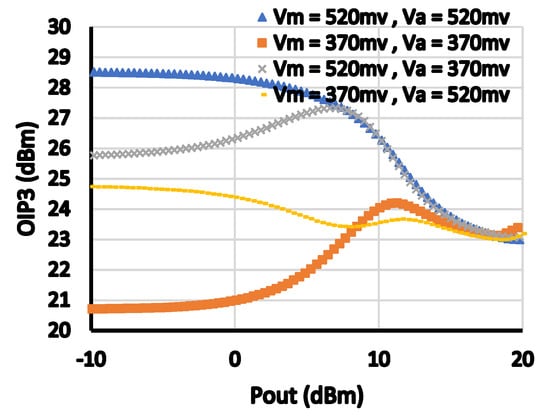
Figure 7.
OIP3 versus Pout for different biasing voltages of main and auxiliary amplifiers.
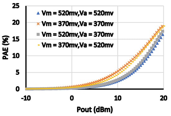
Figure 8.
PAE versus Pout for different biasing voltages of main and auxiliary amplifiers.
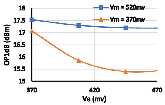
Figure 9.
OP1 dB versus biasing voltages of main and auxiliary amplifiers.
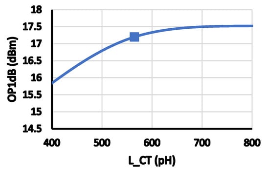
Figure 10.
OP1 dB versus center-tapped output inductance.
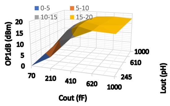
Figure 11.
OP1 dB versus Cout and Lout, at L_CT = 700 pH.
Figure 12 and Figure 13 show the changes in OP1 dB and S21 versus the value of the cascode gate capacitor, Cgate. As depicted, the value of Cgate affects the OP1 dB. This is because the voltage swings at the drain of the cascode devices are divided equally between the voltages across the drain and source terminals of the main and cascode transistors using Cgate. However, the gain is reduced as the value of this capacitance decreases (another trade-off). Figure 14 and Figure 15 show the effect of changing cascode gate biasing voltage on OP1 dB and OIP3. Both OP1 dB and OIP3 are affected because they depend on the non-linear output impedance of the main device.
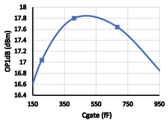
Figure 12.
OP1 dB versus Cgate.
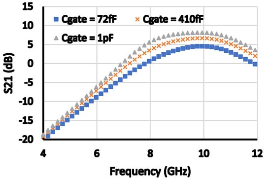
Figure 13.
S21 versus frequency at different values of Cgate.
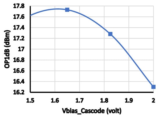
Figure 14.
OP1 dB versus cascode gate biasing voltage.
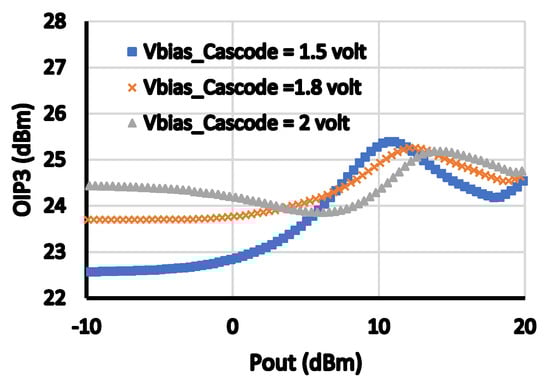
Figure 15.
OIP3 versus Pout at different values of cascode gate biasing voltage.
The sensitivity analysis is summarized in Table 2, which shows the performance specifications and their corresponding design parameters to which they are most sensitive. Based on the above sensitivity analysis and the understanding of the trade-offs between the performance specifications, the proposed design-aware optimization is created.
Table 2.
Performance specifications and their corresponding design parameters.
4.2. The Optimization Flow
The proposed optimization flow used within the tool is presented in Figure 16. The optimization engine uses the BFGS optimization algorithm implemented within the virtuoso environment. The flow relies on five main steps. Below is the explanation of each step and how it is integrated within the tool:
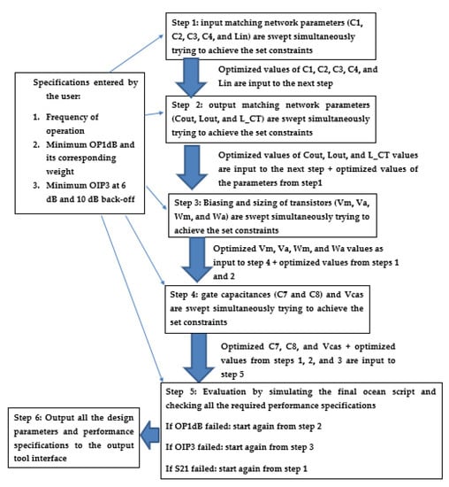
Figure 16.
The proposed optimization flow.
- The user enters the frequency of operation and the required specifications (minimum OP1 dB, minimum OIP3 at 6 dB back off power, minimum OIP3 at 10 dB back-off power and minimum gain (S21)) to the tool web interface. The minimum value of OIP3 at 6/10 dB back-off power will determine the efficiency of the power amplifier. In addition, weights for each targeted design specification are defined.
- The stability of the amplifier is considered as a hard constraint that needs to be met regardless of the performance specifications.
- The initial values of the design parameters need to be defined at the beginning of the optimization. Table 1 shows typical values for those parameters.
- Step 1 in Figure 16: the optimization of the input matching network parameters (C1, C2, C3, C4, and Lin) is carried out. The input to this step is the frequency and performance specifications entered by the user. The optimized values are input to steps 2, 3, 4, and 5.
- Step 2 in Figure 16: the optimization of the output matching network parameters (Cout, Lout, and L_CT) is carried out. The input to this step is the frequency, performance specifications entered by the user, and the optimized parameters from step 1. The optimized values are input to steps 3, 4, and 5.
- Step 3 in Figure 16: the optimization of the biasing and sizing of transistors (Vm, Va, Wm, and Wa) is carried out. The input to this step is the frequency, performance specifications entered by the user, and the optimized parameters from steps 1 and 2. At the end of this step, the modelled parasitic capacitances arising from the transistor layout and its interconnects (Cgs, Cgd, and Cds) are updated corresponding to the optimized widths of the transistors (Wm and Wa). The optimized values are input to steps 4 and 5.
- Step 4 in Figure 16: the optimization of the gate capacitance (C7 and C8) and the cascode gate DC biasing voltage (Vcas) are carried out. The input to this step is the frequency, performance specifications entered by the user, and the optimized parameters from steps 1, 2, and 3. The optimized values are input to step 5.
- Step 5 in Figure 16: it is considered an evaluation point, which determines the next step in the optimization flow.
- If all the specifications (OP1 dB, S21, and OIP3) or (OP1 dB and S21) or (OIP3 and S21) or S21 failed, then the optimization flow is directed to step 1, where the values of the input matching network parameters are being optimized again, then all the rest of the steps will follow in succession. It is to be noted that when step 1 is carried out this time, all the other design parameters have new optimized values that differ from their previous values when step 1 was visited for the first time.
- If (OP1 dB and OIP3) or OP1 dB failed, then the optimization flow is directed to step 2, then all the rest of the steps (3, 4, and 5) will follow.
- If OIP3 failed, the optimization flow is directed to step 3, and then steps 4 and 5 will follow.
- The optimization flow stops when the best achieved design point is obtained based on the pre-defined weighting factors.
- The tool will return back to the web interface: the achieved values for all the required performance specifications, the consumed DC power, PAE at OP1 dB and at 6 dB back-off power, the values of the optimized design parameters, the circuit schematic, a template of the layout of the circuit, and a GDSII file for further modifications.
5. Automation and Test Cases Results
The proposed design tool of the power amplifier is used for automatic sizing. Three test cases are applied at three different frequencies (7, 10, 13 GHz). The 65 nm technology node is used for these test cases. Initially, the user specifies the required performance specifications: frequency of operation, OP1 dB, Gain, and OIP3 at 6 dB back off and 10 dB back off power to the web interface. Weights for different performance specifications are also defined by the user. At the end of the automatic sizing, values of the different design parameters, as well as the achieved performance specifications, are displayed as output. A GDSII layout template for the adopted architecture is also generated.
Figure 17, Figure 18, Figure 19, Figure 20 and Figure 21 show the achieved Pout, OIP3, PAE, AM-AM, and AM-PM distortions and S21 for the three different frequencies (7,10, and 13 GHz). The targeted OP1 dB is higher than 18 dBm, gain is higher than 7 dB, OIP3 is higher than 24 dBm at 6 dB back-off power. As depicted from Figure 17, Figure 18, Figure 19, Figure 20 and Figure 21, the targeted performance specifications are achieved. Table 3 show the required and achieved performance specifications. Finally, Figure 22 shows the layout template of the amplifier which is provided by the proposed design automation tool. A computer with an Intel core i7 processor with 12 GB RAM is used to run this tool.
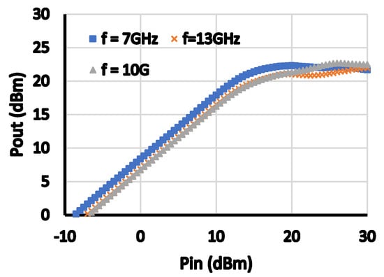
Figure 17.
Pout versus Pin at the three test cases.
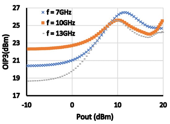
Figure 18.
OIP3 versus Pout at the three test cases.
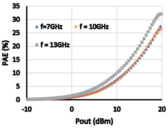
Figure 19.
PAE versus Pout at the three test cases.
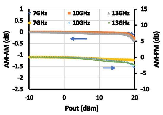
Figure 20.
AM-AM and AM-PM distortion versus Pout at the three test cases.
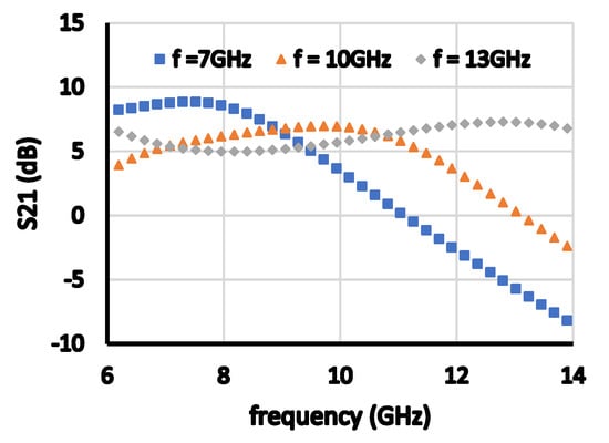
Figure 21.
S21 versus frequency at the three test cases.
Table 3.
The required and achieved performance specifications.
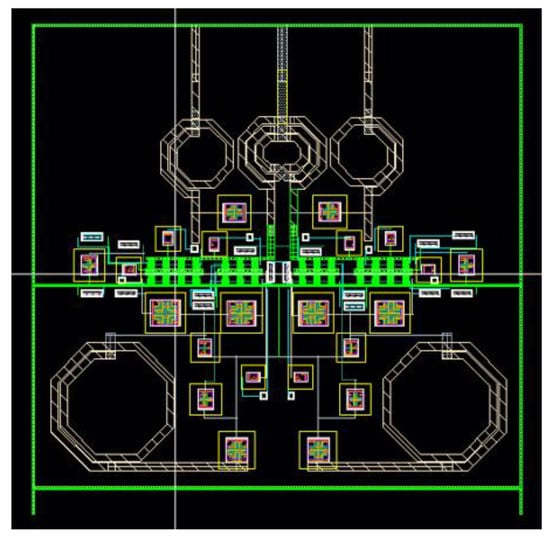
Figure 22.
Layout of the power amplifier.
6. Discussion
The four main aspects that are used in the comparison of the different approaches of RF design optimization and automation are: performance evaluators, inductance modelling, included layout parasitic components and the used optimizers. Table 4 shows a summary of the recent approaches in the sizing and optimization of RF circuits [9].
Table 4.
Summary of the recent approaches in the sizing and optimization of RF circuits.
The performance evaluation is carried out either by using performance models, parametric equations, or circuit simulators. Performance models are inaccurate and must be varied with the variation of circuit topologies [9]. Circuit simulators are the most accurate performance evaluators.
The inductance modelling differs from one approach to another, as shown in Table 4. In the proposed tool, the inductance used is the foundry process design kit (PDK) inductance, modelling the inductance layout parasitic components with high accuracy. Using the PDK inductance model allows the optimization of the physical parameters of the inductance, such as the inner radius and the number of turns to reach the required performance specifications. This results in good estimation of the results of post layout simulations.
Including layout parasitic components in the optimization process differs from one approach to another, as shown in Table 4. In the proposed tool, the post layout simulations of the parasitic extracted view of the transistor along with its interconnects was carried out prior to the optimization process and the resulting parasitic capacitances were included in the optimization process as functions of the sizes of the transistors.
The optimization process differs according to the optimization algorithm used as shown in Table 4. The proposed tool uses BFGS optimizer that is employed by cadence-virtuoso. The BFGS optimizer is used to select the best values of the design parameters that can achieve the required specifications.
7. Conclusions
A parasitic-design-aware simulation-based design tool was proposed for highly linear RF power amplifiers within this paper. Both the optimization steps and design methodology were explained and they rely on the knowledge of the circuit to obtain the design parameters. The proposed tool does not need lengthy simulations when compared to the existing approaches. With parasitic modelling, the design point is close to the final design after layout. The proposed tool was verified to design a highly linear RF power amplifier at three different frequencies (7 GHz, 10 GHz, and 13 GHz) using 65 nm technology node. The results showed that an OP1 dB higher than 18 dBm, gain/S21 higher than 7 dB, and OIP3 higher than 24 dBm at 6 dB back-off power are obtained.
Author Contributions
Conceptualization, R.A.O. and M.E.-N.; formal analysis, R.A.O.; investigation, R.A.O.; methodology, R.A.O.; supervision, M.E.-N. and H.R.; validation, R.A.O.; visualization, R.A.O.; writing—original draft, R.A.O.; writing—review and editing, M.E.-N. All authors have read and agreed to the published version of the manuscript.
Funding
This research received no external funding.
Data Availability Statement
Some of the data presented in this study are available upon request from the corresponding author.
Acknowledgments
The authors would like to thank engineer Ahmed Samir for his remarkable help with the software part of the web tool.
Conflicts of Interest
The authors declare no conflict of interests.
References
- Sajedin, M.; Elfergani, I.T.E.; Rodriguez, J.; Abd-Alhameed, R.; Barciela, M.F. A Survey on RF and Microwave Doherty Power Amplifier for Mobile Handset Applications. Electronics 2019, 8, 717. [Google Scholar] [CrossRef]
- Kim, J.; Lee, C.; Yoo, J.; Park, C. Antiphase Method of the CMOS Power Amplifier Using PMOS Driver Stage to Enhance Linearity. Electronics 2020, 9, 103. [Google Scholar] [CrossRef]
- Mayeda, J.; Lie, D.Y.C.; Lopez, J. Broadband Millimeter-Wave 5G Power Amplifier Design in 22 nm CMOS FD-SOI and 40 nm GaN HEMT. Electronics 2022, 11, 683. [Google Scholar] [CrossRef]
- Cripps, S.C. RF Power Amplifiers for Wireless Communications, 2nd ed.; Artech: Norwood, MA, USA, 2006. [Google Scholar]
- Borel, A.; Barzdėnas, V.; Vasjanov, A. Linearization as a Solution for Power Amplifier Imperfections: A Review of Methods. Electronics 2021, 10, 1073. [Google Scholar] [CrossRef]
- Yan, W.; Liu, C.; Zhou, S.; Wu, Z.; Zhang, J. Design and measurement analysis of Class AB power amplifier. In Proceedings of the 2016 IEEE International Conference on Microwave and Millimeter Wave Technology (ICMMT), Beijing, China, 5–8 June 2016; pp. 849–851. [Google Scholar]
- Joo, T.; Koo, B.; Hong, S. A WLAN RF CMOS PA with adaptive power cells. In Proceedings of the 2013 IEEE Radio Frequency Integrated Circuits Symposium (RFIC), Seattle, WA, USA, 2–4 June 2013; pp. 345–348. [Google Scholar]
- Lu, C.; Pham, A.V.H.; Shaw, M.; Saint, C. Linearization of CMOS Broadband Power Amplifiers Through Combined Multigated Transistors and Capacitance Compensation. IEEE Trans. Microw. Theory Tech. 2007, 55, 2320–2328. [Google Scholar]
- Martins, R.; Lourenco, N.; Passos, F.; Povoa, R.; Canelas, A.; Roca, E.; Castro-Lopez, R.; Sieiro, J.; Fernandez, F.V.; Horta, N. Two-Step RF IC Block Synthesis with Preoptimized Inductors and Full Layout Generation In-the-Loop. IEEE Trans. Comput.-Aided Des. Integr. Circuits Syst. 2018, 38, 989–1002. [Google Scholar] [CrossRef]
- Ramos, J.; Francken, K.; Gielen, G.G.E.; Steyaert, M.S.J. An efficient, fully parasitic-aware power amplifier design optimization tool. IEEE Trans. Circuits Syst. I Regul. Pap. 2005, 52, 1526–1534. [Google Scholar] [CrossRef]
- Gonzalez-Echevarria, R.; Roca, E.; Castro-Lopez, R.; Fernandez, F.V.; Sieiro, J.; Lopez-Villegas, J.M.; Vidal, N. An Automated Design Methodology of RF Circuits by Using Pareto-Optimal Fronts of EM-Simulated Inductors. IEEE Trans. Comput. Des. Integr. Circuits Syst. 2017, 36, 15–26. [Google Scholar] [CrossRef]
- Berkol, G.; Unutulmaz, A.; Afacan, E.; Dündar, G.; Fernandez, F.V.; Pusane, A.E.; Başkaya, F. A two-step layout-in-the-loop design automation tool. In Proceedings of the IEEE 13th International New Circuits and Systems Conference (NEWCAS), Grenoble, France, 7–10 June 2015. [Google Scholar]
- Gupta, R.; Ballweber, B.; Allstot, D. Design and optimization of CMOS RF power amplifiers. IEEE J. Solid-State Circuits 2001, 36, 166–175. [Google Scholar] [CrossRef]
- Liu, B.; Deferm, N.; Zhao, D.; Reynaert, P.; Gielen, G.G.E. An Efficient High-Frequency Linear RF Amplifier Synthesis Method Based on Evolutionary Computation and Machine Learning Techniques. IEEE Trans. Comput. Des. Integr. Circuits Syst. 2012, 31, 981–993. [Google Scholar] [CrossRef]
- Vancorenland, P.; De Ranter, C.; Steyaert, M.; Gielen, G. Optimal RF Design Using Smart Evolutionary Algorithms. In Proceedings of the 37th Annual Design Automation Conference, Los Angeles, CA, USA, 5–9 June 2000; pp. 7–10. [Google Scholar]
- Lberni, A.; Sallem, A.; Marktani, M.A.; Ahaitouf, A.; Masmoudi, N.; Ahaitouf, A. Simulation-Based Optimization for Automated Design of Analog/RF Circuits. In WITS 2020. Lecture Notes in Electrical Engineering; Bennani, S., Lakhrissi, Y., Khaissidi, G., Mansouri, A., Khamlichi, Y., Eds.; Springer: Singapore, 2022; Volume 745. [Google Scholar]
- Liao, T.; Zhang, L. Parasitic-Aware GP-Based Many-Objective Sizing Methodology for Analog and RF Integrated Circuits. In Proceedings of the 2017 22nd Asia and South Pacific Design Automation Conference (ASP-DAC), Chiba, Japan, 16–19 January 2017; pp. 475–480. [Google Scholar]
- Afacan, E.; Dündar, G. A Mixed Domain Sizing Approach for RF Circuit Synthesis. In Proceedings of the 2016 IEEE 19th International Symposium on Design and Diagnostics of Electronic Circuits & Systems (DDECS), Kosice, Slovakia, 20–22 April 2016; pp. 1–4. [Google Scholar]
- Virtuoso Analog Design Environment GXL. Cadence.com. Available online: www.cadence.com/content/dam/cadence-www/global/en_US/documents/tools/custom-ic-analog-rf-design/virtuoso-analog-design-environment-gxl-ds.pdf (accessed on 20 October 2022).
- Spectre RF Option. Cadence.Com. Available online: www.cadence.com/en_US/home/tools/custom-ic-analog-rf-design/circuit-simulation/spectre-rf-option.html (accessed on 10 November 2022).
- Brownlee, J. A Gentle Introduction to the BFGS Optimization Algorithm. Tutorial on Optimization. Available online: https://machinelearningmastery.com/bfgs-optimization-in-python/ (accessed on 19 May 2021).
- Nocedal, J.; Wright, S. Numerical Optimization (Chapter 6), 2nd ed.; Springer: Berlin/Heidelberg, Germany, 2006. [Google Scholar]
- Kang, S.; Baek, D.; Hong, S. A 5-GHz WLAN RF CMOS Power Amplifier with a Parallel-Cascoded Configuration and an Active Feedback Linearizer. IEEE Trans. Microw. Theory Tech. 2017, 65, 3230–3244. [Google Scholar] [CrossRef]
- De Ranter, C.; Van der Plas, G.; Steyaert, M.; Gielen, G.; Sansen, W. CYCLONE: Automated design and layout of RF LC-oscillators. IEEE Trans. Comput. Des. Integr. Circuits Syst. 2002, 21, 1161–1170. [Google Scholar] [CrossRef]
- Zhang, G.; Dengi, A.; Rohrer, R.A.; Rutenbar, R.A.; Carley, L.R. A Synthesis Flow Toward Fast Parasitic Closure for Radio-Frequency Integrated Circuits. In Proceedings of the 41st Annual Design Automation Conference, San Diego, CA, USA, 7–11 June 2004; pp. 155–158. [Google Scholar]
Disclaimer/Publisher’s Note: The statements, opinions and data contained in all publications are solely those of the individual author(s) and contributor(s) and not of MDPI and/or the editor(s). MDPI and/or the editor(s) disclaim responsibility for any injury to people or property resulting from any ideas, methods, instructions or products referred to in the content. |
© 2023 by the authors. Licensee MDPI, Basel, Switzerland. This article is an open access article distributed under the terms and conditions of the Creative Commons Attribution (CC BY) license (https://creativecommons.org/licenses/by/4.0/).