Abstract
A novel reconfigurable transmitarray (RTA) with two-dimensional (2D) wide beam steering capability is presented herein. Different from the traditional RTA with the discrete phase compensation (one-bit or multi-bits phase shift), a second order parallel bandpass filter model is used to realize the RTA elements with a continuous phase compensation. A sandwich structure composed of the two patches with rectangular slots and the middle ground sheet with the cruciform slot is constructed for the phase shift characteristics of the frequency selective surface (FSS), and two varactor diodes are loaded across the rectangular slots on the two top and bottom patches. The simulated results show that the proposed elements could achieve continuous transmission phase compensation from to with a 3 dB insert loss within the operating band of 11.8–12.6 GHz. The RTA prototype with elements and an aperture size of at 12.2 GHz is fabricated and measured for experimental verification. The measured results show that its beam scanning range can reach in both horizontal and vertical planes with a peak gain of 22.76 dBi and a aperture efficiency of 24.65%. Furthermore, the sidelobe levels (SLLs) are lower than −17.8 dB, which is much better than most RTAs. The proposed RTA has potential applications in radar, microwave imaging and wireless communication systems with low-cost fabrication and a stable performance.
1. Introduction
With the continuous development of wireless communication systems, in order to meet the strict requirements of antennas in the fields of remote communication, radar detection and imaging, electronic jamming countermeasures, and so on, it is necessary to develop high-gain antennas with flexible beam scanning capability to compensate for propagation loss and meet the communication needs of serving multiple distributed users simultaneously as well as improving the communication capacity. Traditional phased array antennas [1,2] could realize the beam scanning function and provide excellent radiation performance through massive transmit/receive (TR) modules.
However, a large number of phase shifters and RF front-ends would result in high design complexity and large power consumption. In comparison, parabolic antennas [3] do not need the feed network and are able to realize beam scanning through mechanical rotation, but they have the disadvantage of being large in size and high in profile. Recently, owing to their low-cost and concise structure, reconfigurable reflectarray antennas (RRAs) [4,5,6] and transmitarray antennas (RTAs) [7,8,9,10,11,12,13,14,15,16] have become good candidates in the design of large-aperture beam steering antenna systems.
The reconfigurability can be realized by integrating solid-state control devices in elements such as PIN diodes [7,8,9,10], a microelectromechanical system (MEMS) [11], or varactor diodes [12,13,14,15,16,17] to obtain different phase compensation by changing the current distribution of the electromagnetic radiator and to realize the beam scanning function. RRAs mimic parabolic antennas and make use of the integrated elements to manipulate the reflected phase. Owing to this, the steering beam and the feeding antenna are on the same side of the RRAs, and thus, the obvious blockage effects exist, which prevents its further application to some extent. On the contrary, RTAs could achieve the isolation beam and feeding. RTAs combine the advantages of both lens antenna [18] and microstrip array antenna [19], which utilize spatial feeding and avoid complex feed network.
At present, most of the work focuses on the design of 1-bit RTAs, among which the typical RTA element is the receiver–transmitter structure [7], and the RF power transmission is realized by coupling microstrip lines in between. Furthermore, the improved elements are also used to achieve the dual-polarization RTA [8], and the rotated elements are utilized to improve the operating bandwidth [9]. However, due to the limited discrete-phase resolution of 1-bit elements, the freedom of the electromagnetic manipulation of the transmission phase is restricted, and the aperture efficiency of the RTAs is reduced. Accordingly, 2-bit RTAs by the use of two PIN diodes and MEMS switches could provide a better phase manipulation capability, but the corresponding complexity of the bias circuits and design costs would increase significantly [10,11]. On the other hand, the improvement of the phase resolution is also restricted by only the 2-bit elements.
To improve phase resolution, several RTAs with continuous phase tuning capability have been developed in [12,13,14,15,16]. In [12,13], five layers of active frequency selective surfaces (AFSSs) with integrated varactors are designed, but the capability of the beam scanning is limited. To alleviate the problems, the corresponding equivalent circuit model is used for the design of the RTA element. In [14,15], a band-pass filter model is utilized as the prototype to design RTAs operating at different frequencies, but the aperture efficiency and radiation performance (i.e., scanning range, SLLs) are not satisfactory.
In [16,17], a varactor-based phase shifter using a coupled line structure could provide a continuous phase shift from to . Moreover, two PIN diodes are used to alternatively turn on to generate an additional or phase shift. Although a phase compensation can supply more freedom, the addition of more active devices into the elements leads to a high design complexity and an increased insertion loss, which then become the main hindrance for the continuous phase tuning of RTA elements to offer a better radiation performance. Overall, RTAs exploiting phase shifters loaded by varactors are verified to be an effective design solution to flexibly tune phase. However, several challenges, such as a relatively narrow operating bandwidth, the freedom of phase manipulation and radiation performances (i.e., low aperture efficiency and scanning range), are still needed to be addressed.
Herein, an improved RTA with continuous phase tuning in virtue of the varactors incorporated in the FSS is investigated using theoretical analysis, full-wave simulation and experimental measurements. Firstly, an equivalent circuit model of a second-order bandpass filter is established for the transmission characteristics of the three-layered FSS, and the corresponding RTA element could realize a continuous phase tunability by loading two active varactor diodes. Secondly, the RTAs consisting of elements are fabricated for the measurement. The experimental results show that the proposed RTA could achieve two-dimensional (2D) continuous scanning from to at an operating band of 11.8–12.6 GHz, with a maximum gain of 22.76 dBi and a scanning gain loss of 3.3 dB. Finally, the sidelobe level is lower than −17.8 dB, which is far more than most lower-level RTAs.
2. Antenna Design
In this section, the RTA element is designed based on the equivalent circuit model of a band-pass filter, and realizes the transmission characteristics by loading varactor diodes using the phase shift of FSS.
2.1. Element Design
To comprehend the fundamental operational principles of an RTA and the working mechanism of its unit cell, which is equivalently modeled as a second-order LC filter circuit, a straightforward unit cell design was proposed. The configuration of an active RTA unit cell is demonstrated in Figure 1, which is composed of two F4BTME265 substrates (, tan = 0.0015) and three metallic sheets. The metal patches on the upper and lower surfaces are the radiant elements with one rectangular slot between two patches on the substrates. The middle ground sheet with the cruciform slot is constructed for the phase shift characteristics of the frequency selective surface. Two varactor diodes are loaded between the rectangular patches on the top and bottom.
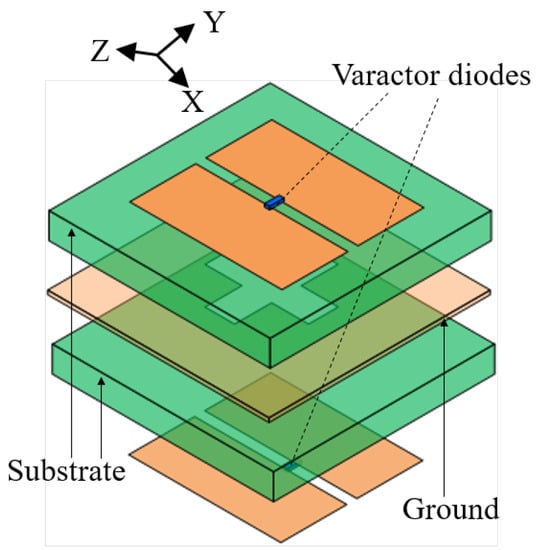
Figure 1.
Configuration of the RTA element.
Under the incidence of the Y-polarized wave, different capacitance values could be obtained by applying different reverse bias voltages to the varactors. From the perspective view from top to bottom, the RTA element is a symmetrical structure with the ground plane in the middle.
Generally, FSS consists of multi-layer elements arranged periodically. The parasitic capacitance and inductance of metal patches printed on the dielectric substrates could be equivalent to parallel LC tanked filters, which would generate band-pass frequency selection response. According to the filter theory, the first-order parallel LC tank circuit would provide a phase delay in the −3 dB passband, the frequency response is shown in Figure 2a, and the phase delay could be realized by cascading two parallel LC tank circuits.
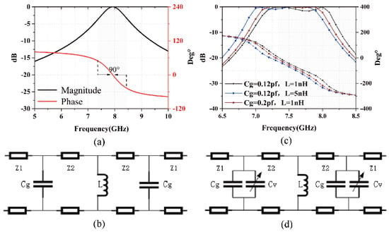
Figure 2.
(a) First-order LC filter with an Advanced Design System (ADS). (b) Second-order bandpass filter equivalent circuit. (c) Different bandpass frequency responses with and . (d) Second-order bandpass filter loadvaractor diode.
The design of an RTA element is constructed according to the second-order bandpass filter circuit as shown in Figure 2b. 1 and 2 are the wave impedance of the free space and the substrate, respectively, is the gap capacitance of the FSS and is the equivalent inductance of the ground. The entire circuit structure is in parallel symmetry form, corresponding to the RTA element.
By changing the values of and , the different responses of the bandpass frequency can be obtained. In order to further verify the correctness of the circuit, the bandpass frequency response of the circuit was calculated in the ADS. As shown in Figure 2c, through an ADS simulation of the proposed circuit, the results indicate that when different values are assigned to and , the variation in the transmission phase and magnitude, with a change in these two parameters, is minimal. Thus, it can be inferred that the circuit can realize the corresponding bandpass frequency response, which can be used as the theoretical basis for the design of the RTA element. However, the reconfigurable characteristics of the RTA element need to be realized by integrating the active device. Figure 2d shows the circuit model after loading varactor diodes, whose center frequency could be tuned using the varactor. According to the equivalent circuit theory, the varactor diodes soldered on the slots of the FSS can be equivalent to the circuits in Figure 3.
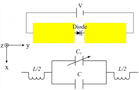
Figure 3.
Equivalent circuit of the proposed FSS.
According to the analysis of a two-port microwave network, it is known that the transmission phase of a unit cell could be expressed by the phase of , i.e., of a two-port network. When the capacitor of varactor is much larger than in the circuit, then the formula could be set up, e.g., . Therefore, in order to obtain the relationship between the transmission phase and the capacitor of varactor , Equations (1)–(3) were employed for calculation. Herein, ADS is used to simulate and verify the equivalent circuit, as shown in Figure 4. It is proven that different transmission phases could be obtained by changing the values of .
where represents the angular frequency, stands for inductance, is the impedance of free space and is the impedance of the dielectric substrate.
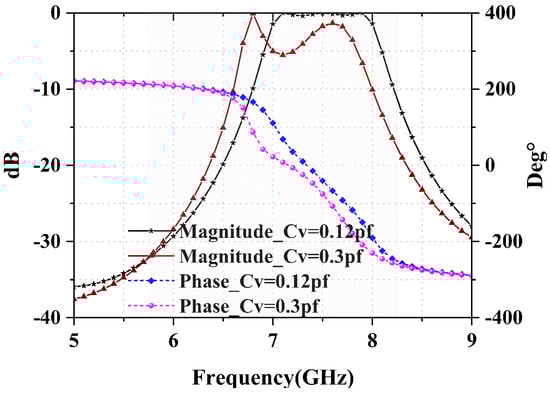
Figure 4.
Transmission phase and magnitude with different .
2.2. Parametric Study
Due to the inherent problem of a limited transmission-phase compensation range for a two-layered RTA element, it is necessary to optimize the structure of the element to further increase the transmission magnitude and the range of the transmission phase. The vertical vias in receive/transmit elements are introduced into the proposed structure, so that an additional direct coupling between the top and bottom radiation patches can be utilized to achieve better performance.
As illustrated in Figure 5a, the initial FSS structure has been subjected to redesign and optimization processes. The patches on the top and bottom layers are now interconnected through two vias. This novel arrangement facilitates the direct transfer of induced currents through the vias, thereby mitigating energy loss in coupling and consequently amplifying both the transmission magnitude and the compensatory range of the transmission phase. Additionally, the V-shaped slots have been introduced along the sides of the FSS, leading to the creation of slot capacitors.
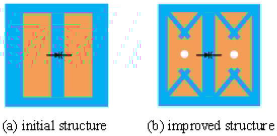
Figure 5.
RTA element structure: (a) initial structure, (b) improved structure.
Due to the serial characteristics inherent to these slot capacitors, the total equivalent capacitance of the circuit correspondingly diminishes. This reduction in capacitance contributes to an increase in the electrical length of the element, subsequently elevating the operating frequency of the element. The combination of these enhancements results in the finalized and reconfigured structure, depicted in Figure 5b. Moreover, the altered configuration simply involves varying the electrical dimensions of the element. Therefore, the equivalent second-order LC filter circuit prototype and the method for calculating the transmission phase in the optimized element structure remain unchanged.
To inspect the properties of the element, numerical simulations are carried out via the commercial full-wave package (CST Studio Suite 3D 2021). Moreover, according to the filter theory, the transmission phase and magnitude are two crucial physical quantities that need to be taken into consideration, and it is clear that the transmission responses of different bandpass frequencies can be obtained by changing and , as shown in Figure 2c. Therefore, based on this circuit analysis, the RTA element is designed and optimized by adjusting the corresponding parameters and to match with the corresponding and in this circuit. The optimized simulation results of and are shown in Figure 6a and Figure 6b, respectively. In Figure 6a, as varies from 1 to 7 mm while keeping at 0.4 mm, and in Figure 6b, as varies from 0.2 to 0.5 mm while keeping at 5 mm, it can be observed that only when is equal to 5 mm and is equal to 0.4 mm that the transmittance remains within a −3 dB variation range, within the frequency range of 11.5 to 12.8 GHz, and it satisfies a phase difference. Additionally, the results show that this RTA element can realize the corresponding bandpass frequency response. Although the structures of the element could be implemented with a standard printed circuit board (PCB) technique, the most technical difficulty during the implementation of the RTA is the layout of the DC bias circuits of the varactors.
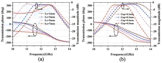
Figure 6.
Different bandpass frequency responses with different (a) and (b) .
To achieve an effective two-dimensional beam scanning, each varactor should be directly supplied with a specified DC voltage, as bias lines would block the transmission of the electric fields illuminating into the FSS. To alleviate this challenge, we chose to set the bias line below the intermediate metallic sheet (i.e., ground) where the electric field is the weakest, and add a bonding film (polypropylene (PP), , tan = 0.004) with a thickness of only 0.118 mm to separate them. Moreover, a sector choke inductor is added to the bias lines to isolate the RF circuit from the DC. The configuration of bias lines is shown in Figure 7. Owing to the existence of ground, the lengths and number of bias lines would not significantly affect the transmission characteristic of the RTA element.
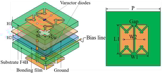
Figure 7.
Implementation of the RTA element. The dimensions are as follows: (units: mm) L1 = 7.2, W1 = 7, W2 = 5.2, Gap = 0.4, P = 12, H1 = 1.524, H2 = 0.118, SL = 2.7 and SW = 1.2.
Herein, the varactor is the MA46H120 from MACOMTM, whose equivalent circuit comprises a series of 0.05 nH inductances, two parallel resistances and a capacitance that can be tuned from 1.2 to 0.18 pf by DC voltages tuning from 0 to 15 V. The simulated transmission results are shown in Figure 8. As shown in Figure 8a, it can be observed that as takes different values, the variations in the curves for circuits with and without bias lines are essentially consistent. Hence, it can be concluded that the transmission phase and amplitude responses remain unaffected by the presence of bias lines. Additionally, it is seen that when is tuned from 0.2 to 0.5 pf, the operating center frequency of the passband moves from 11.5 to 12.8 GHz, and the corresponding phase compensation range is up to at 12.2 GHz, in which the fluctuation of transmission amplitude is kept within 3 dB in Figure 8b. The frequency range for the transmission can be considered as the operating bandwidth of the RTA. By the use of the proposed RTA element above, a 3.2 mm thick low-profile RTA composed of unit cells as well as its DC control boards are designed and implemented as illustrated in Figure 9.
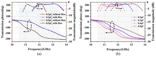
Figure 8.
Transmission phase and magnitude with (a) different with/without bias, (b) changes from 0.2 pf to 0.5 pf.
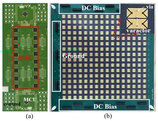
Figure 9.
(a) DC control board. (b) Fabricated reconfigurable transmitarray and Zoomed-in view of the RTA element.
3. Design and Measurement
Figure 9a shows the fabricated DC controlling board, composed of 32-DAC7718s, 4-STM32F103RCT6 microcontroller unit (MCU) and electronic buttons. In order to ensure the compensation precision of continuous phase and reduce the phase errors, 12-bit eight-channel TI DAC7718 chips are used to realize the high-precision bias voltage supply. The output DC bias voltage is controlled in real-time by the integrated button modules via the MCU.
The RTA is constructed using a four-layer metallic hybrid plate as shown in Figure 9b. Figure 9b shows the fabricated RTA; the aperture size of the RTA is about 196 × 196 mm with 256 elements and 512 varactors. The varactor diodes are soldered in the elements on the top and bottom with two vias in the center of the patch. The 16 DC bias sockets are evenly distributed on the left and right sides of the fabricated board, in which each socket consists of 16 bias voltage lines.
Under the free-space measurement, the transmission characteristics of the fabricated RTA is experimentally tested. The RTA is fabricated with the low-cost printed circuit board (PCB) technology. Furthermore, this RTA’s measurements are conducted in a microwave anechoic chamber, utilizing a standard horn antenna as the feeding source, which is positioned at a distance of 135 mm from the transmission array surface, with a focal length-to-diameter ratio (F/D) of 0.7. Simultaneously, an ultra-wideband horn antenna is employed as the receiving antenna for far-field radiation pattern testing. During the testing process, a control circuit is employed to apply varying voltages to the varactor diodes, effectively mimicking different values used in simulation. The measured results are illustrated in Figure 10. It can be observed that when the DC voltage is increased from 0 V to 8 V, the operating frequency of the passband moves from 11.4 to 13 GHz, and the corresponding range of phase tunability is about at 12.2 GHz. When comparing the simulated results in Figure 8b, as is tuned from 0.2 to 0.5 pf, the operational center frequency of the passband shifts from 11.5 to 12.8 GHz, and the corresponding phase compensation range is up to at 12.2 GHz. It is seen that the measured results coincide with the simulated ones, but there are still some deviations of the operating passband frequencies, which is probably caused by the fabricated errors, soldering problem of the large amount of varactor diodes, and so on. Furthermore, according to the literature [14], this type of varactor diodes is reported to work in C-band, but a not in band. Thus, the parameters of lumped RLC in equivalent circuit are not fully accurate, which is the main reason for the deviation of the operating frequencies. Also, due to the insertion loss of the active devices, the transmission loss is slightly larger than the simulated one.
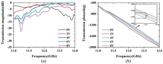
Figure 10.
Measured transmission results of the fabricated RTA (a) magnitude and (b) phase.
According to the transmission characteristics in Figure 10, the distribution of the voltages of DC bias for the RTAs operating at 12.2 GHz is illustrated in Figure 11. The reverse in bias voltage from 0 V to 7.2 V ensures that the transmission magnitude is maintained at about 3 dB and the corresponding phase tunability is about . By directly controlling the DAC via the MCU, the fast beam-forming process could be flexibly manipulated.
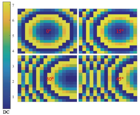
Figure 11.
Voltage distribution with different scanning angles.
Figure 12 shows the measured steering beams at 11.8–12.6 GHz. It can be seen that the RTA could well achieve 2D beam steering from to , and the radiation pattern could remain stable at the whole operating bandwidth. As illustrated in Figure 12b, at 12.2 GHz, the scanning gain loss is within the 3.3 dBi value range, which is close to the simulated ones. Furthermore, the proposed RTA exhibits a low sidelobe level of −17.8 dB, as demonstrated in Table 1. Furthermore, Figure 13 shows the measured beams steered in both horizontal and vertical planes at 11.8, 12.2, and 12.6 GHz, respectively. Figure 14a depicts the radiation patterns of main beam co-polarization and cross-polarization at 12.2 GHz. It can be seen that the cross-polarization performance of the proposed RTA is satisfied with a difference of about 28 dB, between main beam co- and cross-polarization patterns. The maximum gain of the measured main pattern is about 22.76 dBi in Figure 14b, and the corresponding aperture efficiency is 24.65%. The calculation formula of aperture efficiency is as follows:
where is the measured gain of the RTA, is the wavelength at the operating frequency and is the physical area of the RTA.
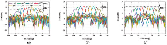
Figure 12.
Measured radiation patterns of RTA at the operating frequencies (a) 11.8 GHz, (b) 12.2 GHz, (c) 12.6 GHz.

Table 1.
Measured/simulated gain, HPBW and SLL at 12.2 GHz.
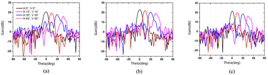
Figure 13.
Measured results both in horizontal (H) and vertical (V) planes at (a) 11.8 GHz, (b) 12.2 GHz, (c) 12.6 GHz.
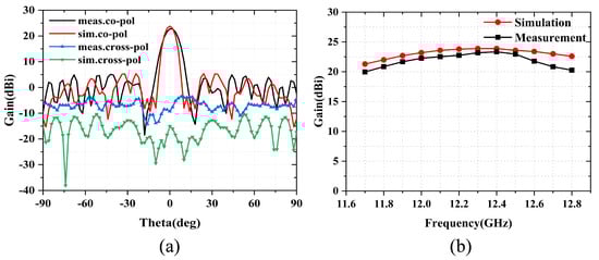
Figure 14.
Simulated and measured (a) boresight and cross-polarization patterns and (b) gains.
The simulated and measured radiation gain versus different frequencies is depicted in Figure 14b. Due to some fabrication issues such as dielectric loss, manufacturing tolerances, and an insertion loss of coaxial cable, the measured gain exhibits slightly lower values than those of the simulated one. Nevertheless, both the simulated and measured gains remain almost stable in the whole operating frequency band. Compared with the recently reported RTAs, the proposed RTA uses only two active devices to achieve high radiation characteristics at a low cost. It shows that two-dimensional beam scanning is performed in 11.8 to 12.6 GHz, and the scanning beam range is . Compared to most RTAs, the lowest sidelobe levels could be achieved with about −15 dB. All the measured results validate that the proposed RTA exhibits an excellent radiation performance.
4. Conclusions
A novel RTA with continuous phase tuning for 2D wide beam scanning application at band is investigated. Based on the design theory of tunable FSS, the RTA element with a three-layer FSS is constructed according to the equivalent structure of the second-order parallel bandpass filter. Two varactor diodes are loaded across the narrow rectangular slots on the two top and bottom patches, and direct coupling using the vias from the top patches to the bottom ones is applied to reduce transmission loss. By applying different reverse bias voltages to the varactors, an almost continuous transmission phase compensation is realized. The RTA composed of elements is fabricated for validation. The measurement of the proposed antenna shows that the continuous 2D beam scanning from to , from 11.8 to 12.6 GHz, could be flexibly carried out using the digital MCU. The beam scanning gain loss could also be less than 3.3 dB. At an operating frequency of 12.2 GHz, the maximum gain of RTA is 22.76 dBi with a sidelobe level of −17.8 dB, and the corresponding aperture efficiency is 24.65%. Compared to the sate-of-the-art work, as shown in Table 2, the proposed RTA exhibits several merits of the radiation performance, such as a wide scanning range, small scanning gain loss and low sidelobe levels. The proposed RTA can be a good candidate for future wireless communication, sensing and imaging applications.
Table 2.
Comparison between various transparent antennas.
Author Contributions
Conceptualization, M.S. and H.X.; methodology, H.X. and K.X.; software, M.S.; validation, H.X.; formal analysis, X.Q.; investigation, H.L.; resources, Q.L.; data curation, S.H.; writing—original draft preparation, H.X.; writing—review and editing, M.S. and K.X.; visualization, S.C. and X.Q.; supervision, W.Z.; project administration, M.S. and H.X.; funding acquisition, X.L., K.X. and W.L. All authors have read and agreed to the published version of the manuscript.
Funding
This work was supported in part by the the National Natural Science Foundation of China under grant no. 61971174 and grant no. 62293493, in part by the Natural Science Foundation of Shanxi Province under grant 2023-JC-QN-0682, and in part by the Zhejiang Provincial Department of Education General Research Fund Project under grant Y202250037.
Data Availability Statement
The data that support the findings of this study are not openly available due to sensitivity but are available from the corresponding author upon reasonable request.
Conflicts of Interest
The authors declare no conflict of interest.
References
- Hashemi, M.; Fikes, A.C.; Gal-Katziri, M. A flexible phased array system with low areal mass density. Nat. Electron. 2019, 2, 195–205. [Google Scholar] [CrossRef]
- Yin, Y.; Ustundag, B.; Kibaroglu, K.; Sayginer, M.; Rebeiz, G.M. Wideband 23.5–29.5 GHz phased arrays for multistandard 5G applications and carrier aggregation. IEEE Trans. Microw. Theory Techn. 2021, 69, 235–247. [Google Scholar] [CrossRef]
- Chakrabarti, S.; Barman, G. An s-/ka-band shared aperture tracking reflector antenna with polarization diversity. IEEE Trans. Antennas Propag. 2021, 69, 3165–3176. [Google Scholar] [CrossRef]
- Wu, F.; Lu, R.; Wang, J.; Jiang, Z.H.; Hong, W.; Luk, K.M. Circularly polarized one-bit reconfigurable ME-dipole reflectarray at x-band. IEEE Antennas Wirel. Propag. Lett. 2022, 21, 496–500. [Google Scholar] [CrossRef]
- Li, H.; Qi, X.; Zhou, T.; Xu, Z.; Denidni, T.A. Wideband reconfigurable reflectarray based on reflector-backed second-order bandpass frequency selective surface. IEEE Trans. Antennas Propag. 2022, 70, 12334–12339. [Google Scholar] [CrossRef]
- Zhou, S.G.; Zhao, G.; Xu, H.; Luo, C.W.; Sun, J.Q.; Chen, G.T.; Jiao, Y.-C. A Wideband 1-Bit Reconfigurable Reflectarray Antenna Ku-Band. IEEE Antennas Wirel. Propag. Lett. 2022, 21, 566–570. [Google Scholar] [CrossRef]
- Wang, M.; Xu, S.; Yang, F.; Li, M. Design and measurement of a 1-bit reconfigurable transmitarray with subwavelength h-shaped coupling slot elements. IEEE Trans. Antennas Propag. 2019, 67, 3500–3504. [Google Scholar] [CrossRef]
- Wang, Y.; Xu, S.; Yang, F.; Werner, D.H. 1 bit dual-linear polarized reconfigurable transmitarray antenna using asymmetric dipole elements with parasitic bypass dipoles. IEEE Trans. Antennas Propag. 2021, 69, 1188–1192. [Google Scholar] [CrossRef]
- Luo, C.W.; Zhao, G.Y.; Jiao, C.; Chen, G.T.; Yan, Y.D. Wideband 1-bit reconfigurable transmitarray antenna based on polarization rotation Element. IEEE Antennas Wirel. Propag. Lett. 2021, 20, 798–802. [Google Scholar] [CrossRef]
- Diaby, F.; Clemente, A.; Sauleau, R.; Pham, K.T.; Dussopt, L. 2-bit reconfigurable unit-cell and electronically steerable transmitarray at ka -band. IEEE Trans. Antennas Propag. 2020, 68, 5003–5008. [Google Scholar] [CrossRef]
- Cheng, C.C.; Lakshminarayanan, B.; Abbaspour-Tamijani, A. A programmable lens-array antenna with monolithically integrated MEMS switches. IEEE Trans. Microw. Theory Tech. 2009, 57, 1874–1884. [Google Scholar] [CrossRef]
- Reis, J.R.; Caldeirinha, R.F.S.; Hammoudeh, A.; Copner, N. Electronically reconfigurable FSS-inspired transmitarray for 2-D beam steering. IEEE Trans. Antennas Propag. 2017, 65, 4880–4885. [Google Scholar] [CrossRef]
- Li, H.; Fan, Y.; Zhuang, Y.; Zhou, T.; Denidni, T.A. Experimental validation of an active parallel-plate-waveguide-loaded metasurfaces lens for wide-angle beam steering. IEEE Antennas Wirel. Propag. Lett. 2022, 21, 2156–2160. [Google Scholar] [CrossRef]
- Ma, C.; Li, H.; Zhang, B.; Ye, D.; Huangfu, J.; Sun, Y.; Zhu, W.; Li, C.; Ran, L. Implementation of a 2-D Reconfigurable Fresnel-Zone Antenna. IEEE Trans. Antennas Propag. 2021, 69, 520–525. [Google Scholar] [CrossRef]
- Xi, Q.; Ma, C.; Li, H.; Zhang, B.; Li, C.; Ran, L. A reconfigurable planar fresnel lens for millimeter-wave 5G frontends. IEEE Trans. Microw. Theory Techn. 2020, 68, 4579–4588. [Google Scholar] [CrossRef]
- Huang, C.; Pan, W.; Luo, X. Low-loss circularly polarized transmitarray for beam steering application. IEEE Trans. Antennas Propag. 2016, 64, 4471–4476. [Google Scholar] [CrossRef]
- Tang, J.; Xu, S.; Yang, F.; Li, M. Design and measurement of a reconfigurable transmitarray antenna with compact varactor-based phase shifters. IEEE Antennas Wirel. Propag. Lett. 2021, 20, 1998–2002. [Google Scholar] [CrossRef]
- Lee, G.H.; Kumar, S.; Choi, H.C.; Kim, K.W. Wideband high-gain double-sided dielectric lens integrated with a dual-bowtie antenna. IEEE Antennas Wirel. Propag. Lett. 2021, 20, 293–297. [Google Scholar] [CrossRef]
- Raeesi, A.; Palizban, A.; Ehsandar, A.; Al-Saedi, H.; Gigoyan, S.; Abdel-Wahab, W.; Safavi-Naeini, S. A Low-Profile 2D Passive Phased-Array Antenna-in-Package for Emerging Millimeter-Wave Applications. IEEE Trans. Antennas Propag. 2023, 71, 1093–1098. [Google Scholar] [CrossRef]
Disclaimer/Publisher’s Note: The statements, opinions and data contained in all publications are solely those of the individual author(s) and contributor(s) and not of MDPI and/or the editor(s). MDPI and/or the editor(s) disclaim responsibility for any injury to people or property resulting from any ideas, methods, instructions or products referred to in the content. |
© 2023 by the authors. Licensee MDPI, Basel, Switzerland. This article is an open access article distributed under the terms and conditions of the Creative Commons Attribution (CC BY) license (https://creativecommons.org/licenses/by/4.0/).