Abstract
The power gain and output power of millimeter-wave (mm-Wave) and terahertz (THz) amplifiers are critical performance metrics, particularly when the operating frequencies of amplifiers are near to the maximum oscillator frequency () of the transistor. This paper presents the design of a 110 GHz amplifier based on the quasi-linear method. The power gain can be boosted to maximum achievable gain () using a linear, lossless, reciprocal feedback network, though this leads to a simultaneous decrease in output power. Based on quasi-linear analysis, for an amplifier with gain, when the K-factor is equal to 1, the output power is zero. To avoid the very low output power of amplifiers, a new approach is proposed to balance power gain and output power. A 110 GHz six-stage feedback amplifier was designed using the proposed approach and fabricated using 40 nm CMOS technology. The measured power gain is 26.5 dB, and the saturation output power is 13 dBm at 110 GHz.
1. Introduction
Millimeter-wave (mm-Wave) and terahertz (THz) frequencies offer vast bandwidth and enable a variety of applications, including ultra-high-speed wireless communication, imaging, and medical sensing [1,2]. Amplifiers play a crucial role in transmitters (TXs) and receivers (RXs). Indeed, with the advancement of modern communication and imaging technologies, there is a strong demand for amplifiers operating in the W-band (75–110 GHz) and beyond [3]. For example, a broadband amplifier with cascaded stagger-tuned stages for 100+ GHz was realized in [4,5,6], introducing a 110–180 GHz broadband amplifier with 10 dB gain and a 70–110 GHz broadband amplifier with over 15 dB gain, respectively. However, when the operation frequency of an amplifier is very high, the gain of the intrinsic transistor is quite low [7,8]. So, previous research has focused on achieving high power gain in mm-Wave and THz.
One of the most useful methods of boosting power gain is to construct feedback networks [9,10,11,12,13,14,15,16,17,18,19,20,21]. As shown in Figure 1, the power gain of a two-port network can achieve the maximum achievable gain by embedding feedback networks. The is only related to the unilateral gain (U, Mason’s invariant), which can be used as a figure of merit to compare any active two-port device. The relationship between the power gain and Rollet’s stability factor (K-factor, K) and U has been researched [9,10,22,23]. The is the peak value of ; we can obtain the amplifier with a gain of or via input and output conjugate matching [12].
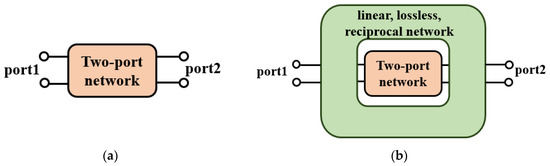
Figure 1.
(a) Basic two-port network. (b) The two-port network of an embedded linear, lossless, reciprocal feedback network.
The work in [18] achieves by boosting gain, but the saturation power is only 0.09 dBm at 247 GHz and −2.36 dBm at 272 GHz. A lossy capacitive over-neutralization technique was proposed to increase U for an amplifier with 14.3 dB of gain and only 1.5 dBm of saturation power [19]. For the feedback amplifier, embedding is used to boost gain and a power combiner is used to increase saturation power in [20,21], which explore inductive gain-boosting power amplifiers to achieve a higher saturation power while maintaining a high . However, this paper does not propose a general method to balance gain and output power. Additionally, the saturation output power of amplifier is not well researched when it is boosted to . Previous research studies focus on the gain in most cases; they ignore the change in output power when K = 1. To investigate this phenomenon, this paper analyzes a two-port network, and a set of formulas are derived based on a quasi-linear model. For feedback amplifiers, the relationship between power gain and K-factor and the relationship between output power and K-factor are all analyzed. These analyses reveal that should not be the design target from the view of trade-off because the saturation output power degrades dramatically. Thus, a new approach is proposed to balance power gain and output power. With the proposed approach, a six-stage differential amplifier was designed and fabricated using 40 nm CMOS technology. The measured results demonstrate a power gain of 26.5 dB and saturation output power of 13 dBm at 110 GHz.
The structure of this paper is as follows: Section 2 presents an analysis of the gain of amplifiers, including the , U, and . Section 3 analyzes the output voltage and power and analyzes the impedance matching and the sensitivity of when K-factor is near to 1, which are all based on the quasi-linear method. Section 4 shows the feedback amplifier design methodology. Section 5 presents the proposed 110 GHz feedback amplifier, which utilizes a novel approach. Section 6 presents the measured results of the fabricated six-stage amplifier. Finally, Section 7 sums up the paper.
2. Gain of Amplifier
2.1. Gma, and K-Factor
A mm-wave and THz amplifier can be modeled as a two-port network for quasi-linear analysis, as shown in Figure 2. Here, the transistor core is modeled as Y-parameters, and the current and voltage on both sides is I1, V1 and I2, V2. The input source is modeled as the current source IS with source admittance YS. In addition, the load admittance is YL.
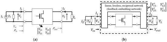
Figure 2.
(a) Quasi-linear model for amplifiers. (b) Quasi-linear model with feedback network for amplifiers.
An amplifier with (maximum available gain, MAG) can be obtained via the simultaneous conjugate impedance matching of input and output if K > 1. For the two-port network, the is the ratio of the power delivered to the load to the power available from the source, and can be derived by the Y-parameters of the two-port network and K-factor, as shown in (1) [23]. This is achieved when input and output impedance matching are simultaneously realized. For an unconditional stable amplifier, its K-factor is more than 1, and only under such conditions can the can be defined. If the operation frequency is quite high and near to fmax, K ≥ 1 is generally satisfied because the gain of transistor is low. The expression of K-factor is shown in (2) [24]. It is important to note that if K < 1, simultaneous conjugate impedance matching cannot be realized.
2.2. Unilateral Power Gain
In electronics, U is a measure of the quality of transistors, which is given in (3) with Y-parameters [24]. The is equal to U when the transistor is unilateralized. Figure 2b shows an example of the quasi-linear model with a feedback network. The feedback embedding network is also modeled as Y-parameters; to distinguish it, it is represented by []. The linear, lossless, reciprocal feedback network does not change the value of U [25].
2.3. Maximum Achievable Gain
is the up limit of , which is shown in (4). The can be boosted to via a linear, lossless, reciprocal feedback network. As (4) shows, is only related with U, so it is also a figure of merit for a given two-port network. In other words, for a given two-port network, the is invariant [25]. Additionally, if U , approaches to 4U, and is 6 dB larger than U. An amplifier with the power gain of can be obtained by tuning the feedback network and conjugate matching the input and output impedance. When designing high-gain amplifiers, gives the guideline for the gain capability at millimeter-wave (mm-Wave) and terahertz (THz) frequency.
2.4. λ-Plane
Define in (5) so that can be shown by K and in (6). It is noted that is complex. The U of a two-port network can be written as a function of and , as shown in (7) [9].
Here, we only consider the unconditional stable (K > 1). Because U is invariant, can be boosted with the change in . In fact, given U and , (7) can be represented as a circle. The -circle will draw on -plane. The function of the -circle is shown in (8).
where and represent the real and imaginary parts of , respectively. The -circle cannot be drawn if K < 1. In order to draw the boundary of the cluster of the -circle, formulas (3) and (5) can be substituted into (1), and the K-factor can be expressed as (9):
Figure 3 shows the -circle and boundary on the -plane. The -plane is employed for amplifier design. According to equation (7), is only related to and U, where U is a constant value. Hence, is solely dependent on . The curve of K = 1 is a teardrop shape as the unconditional stable range (K > 1) is inside the teardrop. All the values should exist in the K > 1 range. The larger is closer to the left apex of the curve. For the , its -circle shrinks into a point. The maximum is realized at the leftmost point on the curve of K = 1, which is the . The leftmost point is on the real axis [17]. Using the graphical approach, it is easy to figure out that can be boosted to under two conditions: (1) if K = 1 and (2) if = 0 [12,13]. Readers who wish to know more can read reference [17].
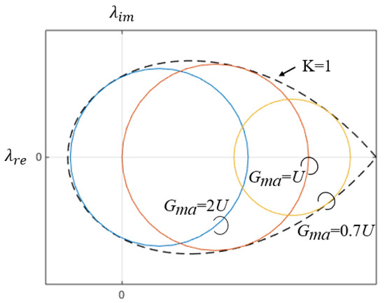
Figure 3.
An example of -plane with the curve of K = 1, = 2U, = U, = 0.7U.
3. Discussion Based on Quasi-Linear Analysis
This section analyzes the linearity and saturation output power when the K approaches 1. Figure 2 is used in the quasi-linear analysis. The following discussion applies to any amplifier and is not limited to feedback amplifiers.
3.1. Output Voltage
Based on the above analysis, if an amplifier needs to achieve the gain of or , simultaneous conjugate impedance matching is necessary for both. Based on the quasi-linear analysis shown in Figure 2, if the simultaneous conjugate impedance matching is realized, the output voltage is shown in (10). The complete derivation of (10) is shown in Appendix A.
It can be observed that K = 1 is a pole for V2. If the K-factor is near to 1, the V2 must be very high, even with small source current Is. However, V2 cannot be very high because it is usually limited by the supply voltage of amplifier. Thus, we can predict that the linearity of amplifier will degrade greatly when the K is approaching 1.
3.2. Output Power
Thus, we can observe input and output power, which are shown as (11) and (12). Generally, the real part of Y22 is not zero. Thus, for a given , the K-factor mainly affects the input and output power values. If K = 1, the input power Pin and output power Pout are zero. This means that the amplifier cannot absorb any power from the source and cannot deliver any power to the load either when K = 1. For a feedback amplifier, if the power gain is boosted to , the input and output power are zero. Thus, cannot be chosen for the design target.
3.3. Impedance Matching
The real part of optimal source impedance ZS_opt is shown as (13). It is zero when K = 1, so the optimal source reflection coefficient ΓS_opt is located on the edge of the Smith chart, which is shown in Figure 4a. In cases where K < 1, achieving simultaneous conjugate impedance matching becomes impossible. This is illustrated in Figure 4b, which depicts S11 and VSWR during conjugate matching; the matching process is close to the edge of the Smith chart. As a result, impedance matching necessitates a high degree of precision. As a result, if the reflection coefficient is located on the edge of the Smith chart, impedance matching to 50 Ohm cannot be realized with lossless components; thus, a lossy impedance matching network must be used. If the power gain is very near to Gmax, the ΓS_opt is very near to the edge of the Smith chart; therefore, we can predict that impedance matching will be difficult to realize and that the impedance matching network will be quite narrow or lossy.
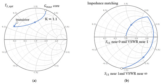
Figure 4.
(a) The optimal source reflection coefficient ΓS_opt on the Smith chart. (b) The and VSWR in the process of impedance matching.
3.4. Sensitivity of
The sensitivity of is analyzed by differentiating with respect to K, and it is found that is sensitive when K near to 1. We derivate the by K to see the slope. The result is shown in (14). It is divided into two terms; the right term is infinite when K = 1. Thus, the value of will be infinite when K = 1. Subsequently, it is impossible for gain to achieve ; the gain will be limited by other conditions.
Figure 5 shows the slope of when K is near 1. degrades dramatically when K is slightly deviating from the 1. This means that is also very sensitive. Our analysis revealed that the gain should not be boosted to . Instead, a trade-off between power gain and output power is proposed.
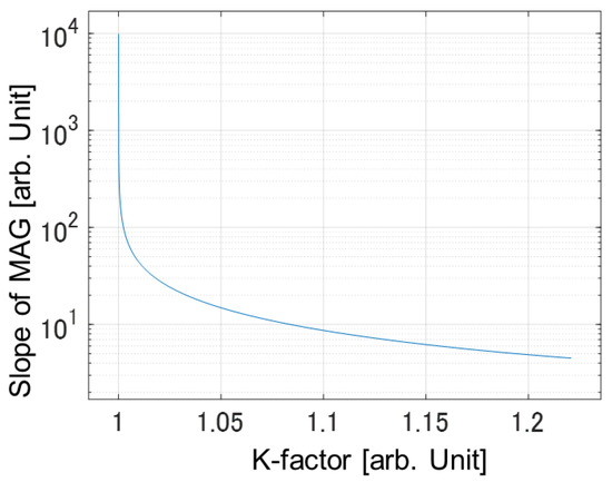
Figure 5.
The slope of versus K-factor. The value becomes infinite when K = 1.
4. Feedback Amplifier Design Methodology
4.1. Boost the Power Gain
Several topologies of the feedback network can boost the power gain to [12,13,14,15,16]. Here, we use the topologies in Figure 6 as an example. Figure 6 shows equivalent single-ended and differential topologies. The feedback admittance -jB for the single-ended topology is equivalent to the jB for the differential configuration. Here, a comprehensive design theory for amplifiers is taken into account, including the consideration of stability. The amplifiers of the proposed two topologies are unconditionally stable. Regarding the two-port network, in this example, the embedding structure is parallel and cascade embedding. Cascade embedding, which is formed by and , can expand the scope of movement on the λ plane. In the single-ended topology, a series of connections involving the inductor and capacitor forms the negative parallel feedback susceptance −jBf. By the equivalent analysis of the two topologies, the cross-coupling of two capacitors forms parallel embedding, and the parallel feedback susceptance is reversed to jBf. We assume that the source and load impedance are simultaneous conjugate impedance matching so that the power gain is . The design process is demonstrated on a six-stage amplifier in Section 5. An NMOS (32 μm/40 nm in size) is created via a 40 nm bulk CMOS process. The fmax of the NMOS is about 275 GHz. The design frequency is 110 GHz. The U is 8.9 dB.
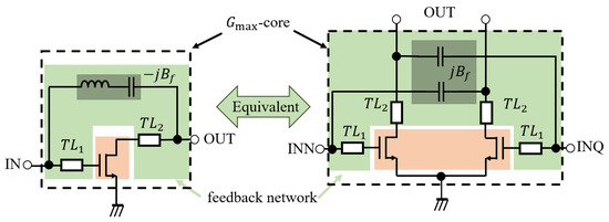
Figure 6.
Single-ended and differential topology for boosting the power gain to Gmax.
It is convenient and intuitive to design a feedback network on the λ plane [10,17]. The power gain of single-ended and differential intrinsic transistors can also be boosted to core via the feedback network. Figure 7 shows the gain boosted on the λ plane. Each capacitor and inductor on the feedback network can change the point location. The change in feedback network can be reflected on the λ plane via the following formula: λ =. We can judge the of an amplifier by analyzing how far the point of is from the point of the core. is 8.8 dB without a feedback network, and the is 14.6 dB.
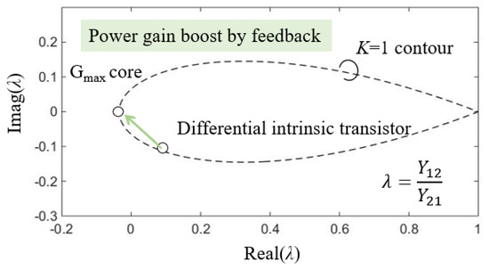
Figure 7.
Gain boosted shown on the λ plain at 110 GHz.
4.2. PG Product
We have analyzed the method used to boost the power gain. The current and voltage will increase faster when K is near to 1 until they reach the limit. Naturally, based on the above analysis, the output power is the next object to be discussed.
Using quasi-linear analysis and BSIM4 model analysis, simulate the saturation power. The quasi-linear analysis is formulated utilizing Y-parameters, while the BSIM4 model is a form of the SPICE model. Distinct modeling approaches account for the variance between the quasi-linear analysis and the BSIM4 model. The BSIM4 model takes the physical characteristics of the transistor into greater consideration. The simulation transistor has a channel length of 40 nm, and its total width is 32 μm when the multiplier is 4. Figure 8 shows the simulation result at 110 GHz, and the result using the BSIM4 transistor model is also shown for comparison. As predicted by (17) and (19), the saturation output power drops very quickly when K is approaching to 1. As the value of K deviates from 1, the saturation output power exhibits a relatively consistent stability. As depicted in Figure 8, under the same conditions, the saturation output power of the BSIM4 model is higher than that of the quasi-linear model. Nevertheless, when K approaches the vicinity of 1, both model outputs experience a rapid decrease in output power.
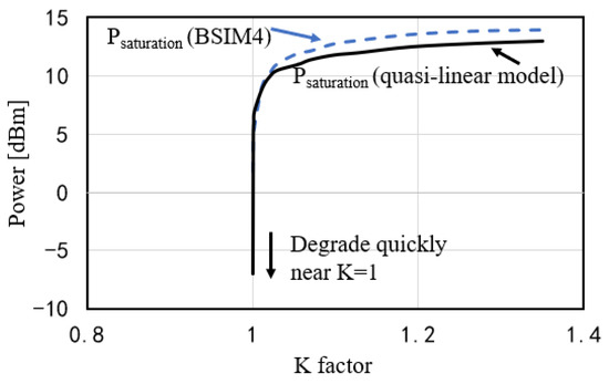
Figure 8.
Simulated saturation output power versus K-factor at 110 GHz.
Based on the discussion above, it is not wise to boost the power gain very near to Gmax, so we would like to discuss the trade-off between the gain and output power. In order to create a more accurate representation of the actual situation, the simulation is based on a large signal with the differential topology. The saturation power versus Gma is drawn in Figure 9. The parallel slashes are the contour lines of the product (PG product), the step of which is 10. The PG products on the same contour lines are equal, and their calculation formulas are shown in the figure. A substantial PG product is attainable only when both and values are elevated. Through assessing the PG product, we can effectively achieve a balance between and . Furthermore, the PG product can be calculated with varying coefficients based on the actual circumstances.
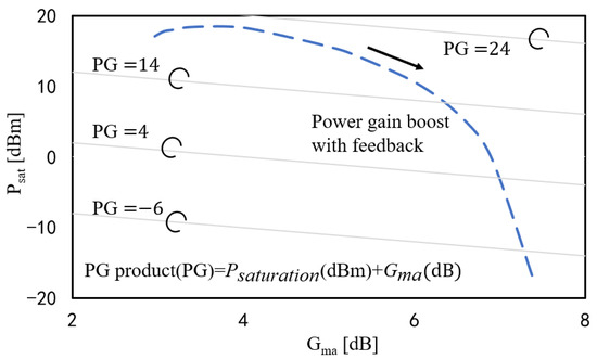
Figure 9.
Saturation output power versus Gma. The parallel slashes are the contour lines of the PG product.
If the PG product is considered as a kind of figure of merit (FoM), the gain boosting can be observed from a different angle. The gain boosting is relatively light on the left side of the cure, and the PG product does not suffer large decreases. The PG product decreases quickly when the gain boosting becomes heavy.
The closer the K-factor gets to 1, the higher Gma is. For the design of the amplifier, the K-factor should be near to 1 but not too close. For the output power, we do not want the PG product to degenerate when the gain is boosted. Thus, from the view of output power management, the curve that shows when the PG product starts to decrease is the design target. Here, the curve simulated with BSIM4 should be used.
5. Six-Stage Feedback Amplifier
5.1. The Last Output Stage
The former stage should provide enough power for the latter stage. In the proposed six-stage amplifier, the total width of the transistors in the last three stages is gradually increasing. Generally, the design of the last stage is particularly important. Its output power and stability can heavily affect the performance of the entire amplifier. Given that the purpose of this stage is to deliver sufficient output power, in accordance with the PG product, we need to compromise some gain values. The size of the transistor is 32 μm/40 nm, with a total of 32 fingers and a multiplier of 4.
Figure 10a illustrates the variation in Gma and saturation output power as the feedback capacitor changes, where Cf represents the feedback capacitor. Due to the wide range of saturation output power variations, a coefficient of 4 is applied to Gma in order to ensure result coherence, resulting in the formula PG product = . Figure 10b shows the PG products versus different feedback capacitors. With a cross-coupling capacitor of 15.7 fF, there is a maximum PG product, making it suitable for constructing the feedback network. When the feedback capacitor is 15.7 fF, the calculated Gma is 5.8 dB, with a saturation output power of 15 dBm at 110 GHz. At this point, the saturation power does not experience a rapid decrease, indicating the effectiveness of our design.
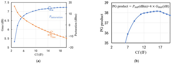
Figure 10.
(a) The Gma and saturation output power versus feedback capacitors. (b) PG products versus different feedback capacitors.
5.2. The Entire Amplifier
A 110 GHz feedback amplifier was designed using the proposed approach. The main targets for designing the amplifier include the output power and gain. The size of the output stage transistor determines the output power, while the number of stages affects the gain of the amplifiers. The design is based on the trade-off between power gain and output power, as quantified by the PG product. Figure 11 shows a schematic of the proposed amplifier; it consists of six pseudo-differential stages. Based on the equivalent relationship between the single-ended and differential topologies from Section 4.1, two single-ended circuits form the pseudo-differential NMOS pair. The feedback network is embedded onto the pseudo-differential pair using cross-coupling capacitors. All stages use the λ plane approach to enhance gain and balance output power according to the PG product. The cross-coupling capacitors are linear, lossless, reciprocal feedback networks, which are used to move the Gma point on the λ plane. There are three terms for why the feedback network only uses the capacitors in the proposed structure. First, from Section 4.2, the Gmax is not the target of boosting gain. It is not necessary nor wise to achieve Gmax accurately. Second, the feedback capacitor can provide sufficient moving range on the λ plane in the process of the proposed amplifier design. Third, the inductor will occupy a large area in the layout. In order to control the area of the amplifier chip, we only select the capacitor to form a feedback network.
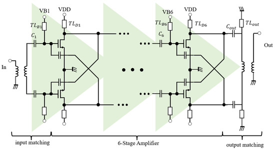
Figure 11.
Schematic of the amplifier that balances power gain and output power.
The capacitor between the two stages of amplifier and transmission line constitutes the inter-stage matching; for example, and constitute the inter-stage matching between the fifth and sixth stages. By tuning inter-stage matching, we can moderate the K-factor and output power of every stage. Additionally, this capacitor can also isolate the DC current. The supply voltage VDD is 1 V, and VB is 0.75 V. The gate and drain terminal voltage of the transistor are tuned and controlled by a transmission line with a characteristic impedance of 50 ohm.
The proposed amplifier design is separated into two parts. The first three stages are seized for gain where the NMOS size is 16 μm/40 nm, and the last three stages are seized for output power, where the NMOS sizes are 32 μm/40 nm, 64 μm/40 nm, and 128 μm/40 nm, respectively. Thus, the goals of the feedback networks for the two parts are also different. For the first three stages, the feedback capacitor is 4.6 fF in simulation. The fourth and fifth stages have a feedback capacitor that is 13.6 fF. The sixth stage of the amplifier utilizes a feedback capacitor with 15.7 fF.
The input and output impedance matching networks are also included in the design schematic shown in Figure 11. The transmission line , capacitor , and balun constitute the input matching. The output matching consists of three parts, namely , parallel transmission lines , and balun.
6. Measurement
The proposed amplifier was fabricated via a 40 nm 10-Metal CMOS process and occupies an area of 820 × 950 (0.779). Its micrograph is shown in Figure 12. The chip was measured on wafer. The input and output were probed using the Cascade Infinity WR8 waveguide probe. Keysight PNA-X and VDI mm-Wave extender were used to measure the S-parameters. The measured result includes the input and output pads. The measured and simulated results of the S-parameters are shown in Figure 13. The peak gain is 26.5 dB at 112 GHz. is −18.5 dB at 102 GHz, and is −12.8 dB at 118 GHz. The measured bandwidth is 14 GHz (from 104 GHz to 118 GHz). Due to the decreases in input, output matching, balun, and transmission lines, the peak of is 7.8 dB lower than the simulated S-parameters.
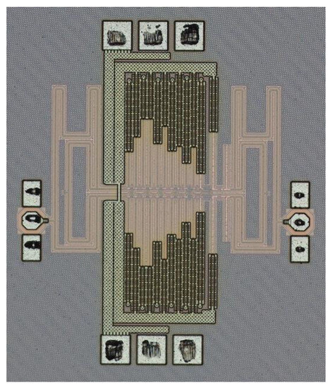
Figure 12.
Photo of the proposed amplifier’s chip.
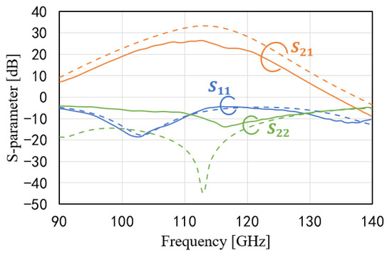
Figure 13.
The measured and simulated S-parameters of the designed amplifier. The simulated parameters are represented by dashed lines, and the measured parameters are represented by solid lines.
The output power was measured using a power meter (Keysight PM5). As Figure 14 shows, the measured saturation power is 13 dBm, and the measured DC power consumption is 182 mW. Although the simulated circuit characteristics and actual circuit characteristics are different. The measured results demonstrate the effectiveness of the proposed design approach in achieving a trade-off between power gain and output power. Table 1 summarizes the measured results in this work and shows a comparison with other state-of-the-art amplifiers.
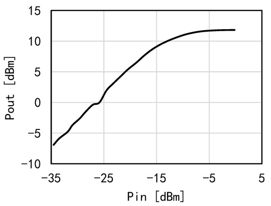
Figure 14.
The measured output power.

Table 1.
Performance summary for the proposed amplifier and comparison with state-of-the-art amplifiers.
7. Conclusions
For this paper, a 110 GHz six-stage CMOS power amplifier was designed and measured, considering the trade-off between power gain and output power. The power gain of the amplifier was discussed based on quasi-linearity analysis. We found that there are many demerits if the power gain is boosted to the Gmax. To overcome the drawback of the Gmax-core design method in the design power amplifier, a design approach based on the × Gma product was proposed so that a suitable trade-off between power gain and output power could be realized. To demonstrate the design method, a 110 GHz six-stages CMOS amplifier was designed. The fabricated amplifier realized a small-signal-power-gain of 26.5 dB and a saturation output power of 13 dBm at 110 GHz. The proposed amplifier is expected to have applications in mm-Wave and THz radar and communications systems.
Author Contributions
Conceptualization, R.D. and Y.X.; methodology, Y.S. and Y.X.; software, Y.S.; validation, R.D. and Y.S.; investigation, R.D., Y.S. and Y.X.; writing, Y.S.; supervision, R.D. All authors have read and agreed to the published version of the manuscript.
Funding
Our research was performed at the Chinese Academy of Science Terahertz Science Center and was funded by the National Natural Science Foundation of China (No. 61988102), the Science and Technology Planning Project of Guangdong Province, China (No. 2019B090909011), the Key Research and Development Program of Guangdong Province, China (No. 2019B090917007), and the Guangzhou Basic and Applied Basic Research project (No. 2023A04J0334).
Data Availability Statement
All data used for this work can be made available upon reasonable request by contacting the corresponding author.
Conflicts of Interest
The authors declare no conflict of interest.
Appendix A
Based on Figure 2, the output current can be expressed as (A1a) and (A1b), which are based on Y-parameter.
It is easy to know V1 = IS/(YS + Yin), so the V2 can be express as (A3).
The input admittance Yin can be expressed the formula as shown in (A4). If it is substitute into (A3), the V2 can be expressed as (A5).
When the simultaneous conjugate impedance matching is realized, the source impedance and the load impedance are labeled with YS_opt and YL_opt, respectively, which are shown in (A6a) and (A6b) [25],
References
- Siegel, P.H. Terahertz technology. IEEE Trans. Microw. Theory Tech. 2002, 50, 910–928. [Google Scholar] [CrossRef]
- Huang, K.; Wang, Z. Terahertz terabit wireless communication. IEEE Microw. Mag. 2011, 12, 108–116. [Google Scholar] [CrossRef]
- Weber, R.; Cwiklinski, M.; Wagner, S.; Lozar, R.; Massler, H.; Bruckner, P.; Quay, R. A Beyond 110 GHz GaN Cascode Low-Noise Amplifier with 20.3 dBm Output Power. In Proceedings of the 2018 IEEE/MTT-S International Microwave Symposium—IMS, Philadelphia, PA, USA, 10–15 June 2018. [Google Scholar]
- Kim, J.; Buckwalter, J.F. Staggered Gain for 100+ GHz Broadband Amplifiers. IEEE J. Solid-State Circuits 2011, 46, 1123–1136. [Google Scholar]
- Chen, P.H.; Kao, J.C.; Yu, T.L.; Hsu, Y.W.; Teng, Y.M.; Huang, G.W.; Wang, H. A 110–180 GHz broadband amplifier in 65-nm CMOS process. In Proceedings of the 2013 IEEE MTT-S International Microwave Symposium Digest (MTT), Seattle, WA, USA, 2–7 June 2013. [Google Scholar]
- Kobayashi, K.W.; Kumar, V. A Broadband 70–110-GHz E-/W-Band LNA Using a 90-nm T-Gate GaN HEMT Technology. IEEE Microw. Wirel. Compon. Lett. 2021, 31, 885–888. [Google Scholar] [CrossRef]
- Shinohara, K.; Corrion, A.; Regan, D.; Milosavljevic, I.; Brown, D.; Burnham, S.; Willadsen, P.J.; Butler, C.; Schmitz, A.; Wheeler, D.; et al. 220GHz fT and 400GHz fmax in 40-nm GaN DH-HEMTs with re-grown ohmic. In Proceedings of the 2010 International Electron Devices Meeting, San Francisco, CA, USA, 6–8 December 2010. [Google Scholar]
- Urteaga, M.; Pierson, R.; Rowell, P.; Jain, V.; Lobisser, E.; Rodwell, M.J.W. 130nm InP DHBTs with ft>0.52THz and fmax>1.1THz. In Proceedings of the 69th Device Research Conference, Santa Barbara, CA, USA, 20–22 June 2011. [Google Scholar]
- Xu, Z.; Xie, Q.; Wang, Z. A Study of Collaborative Gain/Noise Optimization for LNAs at Near-Frequencies Based on a Novel Gain-Noise Plane Approach. IEEE Trans. Circuits Syst. II Express Briefs 2023, 70, 51–55. [Google Scholar] [CrossRef]
- Singhakowinta, A.; Boothroyd, A.R. Gain capability of two-port amplifiers. Int. J. Electron 1966, 21, 549–560. [Google Scholar] [CrossRef]
- Momeni, O. A 260GHz amplifier with 9.2dB gain and –3.9dBm saturated power in 65nm CMOS. In Proceedings of the 2013 IEEE International Solid-State Circuits Conference Digest of Technical Papers, San Francisco, CA, USA, 17–21 February 2013. [Google Scholar]
- Bameri, H.; Momeni, O. A high-gain mm-wave amplifier design: An analytical approach to power gain boosting. IEEE J. Solid-State Circuits 2017, 52, 357–370. [Google Scholar] [CrossRef]
- Wang, Z.; Heydari, P. A study of operating condition and design methods to achieve the upper limit of power gain in amplifiers at near- fmax frequencies. IEEE Trans. Circuits Syst. I 2017, 64, 261–271. [Google Scholar] [CrossRef]
- Park, D.; Utomo, D.R.; Lam, B.H.; Lee, S.; Hong, J. A 230-260-GHz wideband and high-gain amplifier in 65-nm CMOS based on dual-peak Gmax-core. IEEE J. Solid-State Circuits 2019, 54, 1613–1623. [Google Scholar] [CrossRef]
- Dong, R.; Katayama, K.; Takano, K.; Lee, S.; Yoshida, T.; Amakawa, S.; Fujishima, M. 79–85 GHz CMOS Amplifier with 0.35 V Supply Voltage. In Proceedings of the 13th European Microwave Integrated Circuits Conference, Madrid, Spain, 23–25 September 2018. [Google Scholar]
- Xing, Y.; Dong, R. Graphical Approach to Optimization of Maximally Efficient-Gain-Boosted Feedback Amplifiers. Electronics 2023, 12, 2895. [Google Scholar] [CrossRef]
- Amakawa, S.; Ito, Y. Graphical approach to analysis and design of gain-boosted near-fmax feedback amplifiers. In Proceedings of the 2016 46th European Microwave Conference (EuMC), London, UK, 4–6 October 2016. [Google Scholar]
- Park, D.W.; Utomo, D.R.; Yun, B. Design of High-Gain Sub-THz Regenerative Amplifiers Based on Double-Gmax Gain Boosting Technique. IEEE J. Solid-State Circuits 2021, 56, 3388–3398. [Google Scholar]
- Simic, D.; Reynaert, P. Analysis and Design of Lossy Capacitive over-Neutralization Technique for Amplifiers Operating near fmax. IEEE Trans. Circuits Syst. I Regul. Pap. 2021, 68, 1945–1955. [Google Scholar]
- Bameri, H.; Momeni, O. An Embedded 200 GHz Power Amplifier with 9.4 dBm Saturated Power and 19.5 dB Gain in 65 nm CMOS. In Proceedings of the 2020 IEEE Radio Frequency Integrated Circuits Symposium (RFIC), Los Angeles, CA, USA, 4–6 August 2020. [Google Scholar]
- Xinyan, T.; Johan, N.; Alaaeldien, M.; Khaled, K.; Akshay, V.; Björn, D.; Piet, W. Design of D-Band Transformer-Based Gain-Boosting Class-AB Power Amplifiers in Silicon Technologies. IEEE Trans. Circuits Syst. I: Regul. Pap. 2020, 67, 1447–1458. [Google Scholar]
- Singhakowinta, A.; Boothroyd, A. On linear two-port amplifiers. IEEE Trans. Circuit Theory 1964, 11, 169. [Google Scholar] [CrossRef]
- Chen, W.-K. Active Network Analysis: Feedback Amplifier Theory, 2nd ed.; WSPC: Chicago, IL, USA, 2016. [Google Scholar]
- Rollett, J. Stability and power-gain invariants of linear two ports. IRE Trans. Circuit Theory 1962, 9, 29–32. [Google Scholar] [CrossRef]
- Mason, S.J. Power gain in feedback amplifier. IRE Trans. Circuit Theory 1954, 1, 20–25. [Google Scholar] [CrossRef]
- Wu, W.; Chen, R.; Chen, S.; Wang, J.; Chen, L.; Zhang, L.; Wang, Y. A Compact W-Band Power Amplifier with a Peak PAE of 21.1% in 65-nm CMOS Technology. IEEE Microw. Wirel. Technol. Lett. 2023, 33, 703–706. [Google Scholar] [CrossRef]
- Romstadt, J.; Lammert, V.; Pohl, N.; Issakov, V. Transformer-Coupled D-Band PA with 11.8 dBm Psat and 6.3% PAE in 0.13μm SiGe BiCMOS. In Proceedings of the 2020 IEEE 20th Topical Meeting on Silicon Monolithic Integrated Circuits in RF Systems (SiRF), San Antonio, TX, USA, 26–29 January 2020. [Google Scholar]
- Elazar, T.; Socher, E. 95GHz 13dBm IQ-combined PA in 65nm CMOS. In Proceedings of the 2020 50th European Microwave Conference (EuMC), Utrecht, The Netherlands, 12–14 January 2021. [Google Scholar]
Disclaimer/Publisher’s Note: The statements, opinions and data contained in all publications are solely those of the individual author(s) and contributor(s) and not of MDPI and/or the editor(s). MDPI and/or the editor(s) disclaim responsibility for any injury to people or property resulting from any ideas, methods, instructions or products referred to in the content. |
© 2023 by the authors. Licensee MDPI, Basel, Switzerland. This article is an open access article distributed under the terms and conditions of the Creative Commons Attribution (CC BY) license (https://creativecommons.org/licenses/by/4.0/).