Abstract
This paper presents a voltage-controlled delay unit (VCDU) with a novel architecture allowing for a wide input range of linearity and an improved immunity to electromagnetic interferences. The circuit is based on a current-starved inverter with a biasing technique to extend the input voltage range of linearity near to the rail-to-rail linearity range. The proposed scheme was designed by UMC 180 nm standard CMOS process and works without power-hungry amplifiers or comparators. It has a voltage supply of 1.8 V and exhibits a rail-to-rail linearity range (0–1.8 V) with an average EMI-induced jitter of only 1% of the nominal delay.
1. Introduction
Voltage and geometry scaling in CMOS technology have a detrimental effect on analog circuits while on the other hand, they increasingly improve the performances of digital circuits. Therefore, in many applications, it is preferred to implement the entire circuit in the digital domain to increase its reliability. This new approach is illustrated, for example, in [1,2,3,4], where analog functions, such as those of operational transconductance amplifiers (OTAs) amplifying, voltage reference and data converters are obtained by means of true digital circuits. Recently, another interesting idea to build more digitally friend circuit blocks is the use of delay-based signals. This technique exploits the time difference between two signals as analog information. This interesting approach is called time-mode signal processing (TMSP), which means that the amplitude of a signal is represented by means of a time delay [5,6]. Several circuits can be implemented using the building blocks of the TMSP. Indeed, a set of these general components can perform the most basic mathematical operations in the time-mode. Therefore, by arranging these basic structures, a sampled-data infinite impulse response (IIR) filter can be realized. Time-mode circuits are also suitable for precise time measurements, such as in the phase detector used in digital phase locked loop (PLL) [7] or in the circuits measuring the time of flight [8]. In all these architectures, delay generators are the key elements in the analog-to-digital conversion. The delay line, which is the core of the delay generator, is able to retard the input signal by a predefined value, which is fixed or tunable by both an analog or a digital mechanism. The digital mechanism is used for rough tuning while the analog is used for precise delay variation. The most important characteristics of the delay lines are: the finest incremental delay step, the delay range, the linearity and the jitter. The delay can be controlled by changing the power supply voltage or by means of current-starved inverters (tuning their quiescent current). A major challenge in the design of TMSP circuits is to implement a tunable delay cell having a linear transfer characteristic. For example, both the solution based on changing the supply voltage or based on current-starved inverters, although widely used, cannot assure linearity, as shown in Figure 1. Moreover, another drawback is the excessively large increase in delay when the supply voltage (or the gate–source voltage of the current-starved transistor) becomes excessively low. Another approach [9] is based on the modulation of the transistor threshold voltage and hence, the delay is obtained by applying a small-signal analog input to the back-gate, but this solution also presents a nonlinear transcharacteristic because the threshold voltage varies with the input in a square-root fashion, and hence the delay is nonlinear.
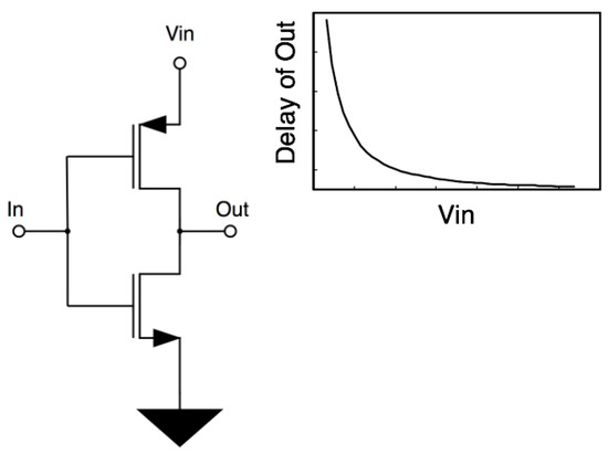
Figure 1.
Schematic of a simple inverter and its delay–voltage characteristic.
Another issue in practically all electronic circuits is the susceptibility to electromagnetic interferences (EMI). EMI effects may indeed involve any electrical or electronic equipment. As an example, aircrafts are especially susceptible to radiated and conducted interferences; in automotives, engines may stall because of the interference induced by traffic lights and cellular telephone transmitters can induce disturbances in braking systems (ABS). In general, as shown in Figure 2, electromagnetic compatibility issues can be divided into two parts: emissions and susceptibility. Both of these should be as low as possible. On the other hand, high emissions are generally caused by high frequencies and high power systems, for example, as in the case of switching converters and motors while the susceptibility is a critical issue in practically all circuits. The integrated circuit ICs can be victim of conducted interferences: indeed, considering their small sizes, ICs are typically not disturbed by radiated EMI, as their on-chip interconnections are excessively small to function as effective antennas. They are, however, subjected to conducted interference which is received by the printed circuit board (PCB) tracks to which they are connected. Conducted EMI can be injected through the I/O pins generally causing two harmful effects: nonlinear distortion and EMI-induced DC bias shift, which can eventually lead to failures [10,11,12]. This is particularly critical in analog ICs but the effect of conducted EMI has also recently been investigated in digital subsystems, and especially in those emulating analog functions such as in digitally based amplifiers or in time-mode circuits. The latter can indeed be susceptible to interferences. In particular, in the voltage-controlled delay unit, the effect of interferences is a strong variation of the delay, which can be named EMI-induced jitter [13,14].
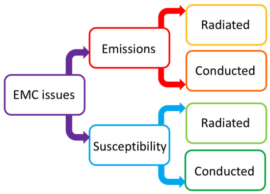
Figure 2.
Electromagnetic compatibility issues.
In this paper, a voltage-controlled delay unit is proposed, with a rail-to-rail linearity range and reduced jitter caused by the electromagnetic interferences’ EMI.
The paper is organized as follows: in Section 2 state-of-the-art VCDUs with increased linearity are outlined; in Section 3, the proposed VCDU with a rail-to-rail range of linearity is presented; in Section 4, the effect of the interferences injected into the I/O pins is discussed; finally, Section 5 concludes the paper.
2. The Voltage-Controlled Delay Units with Increased Linearity Range
The key element of the time-mode signal processing circuits is the voltage-controlled delay unit (VCDU): it is a circuit that proportionally delays an input time event (i.e., a clock edge) with respect to a control voltage . As stated above, one of the most used schematics of VCDU is the one based on the current-starved inverter [5] which is shown in Figure 3. It generally operates as follows: when is low, the capacitor is charged to the supply voltage and is therefore forced to a low logic value. When the input signal goes up, the capacitor starts to discharge itself at a rate which is a function of . The second inverter operates as a comparator: when the voltage of the capacitor drops below the threshold of the inverter, switches from a low to high value. The low-to-high transition time is adjusted by the voltage .
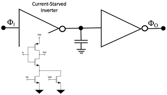
Figure 3.
Schematic of the classical VCDU based on current-starved CMOS inverter [5].
The delay unit based on the current-starved inverter is attractive for its capability to give a wide range of delay. On the other hand, the delay is a nonlinear function of the control voltage . The voltage–delay characteristic of the cell can indeed be written as where is the delay, C is the load capacitance and i is the current controlled by . The current follows the MOSFET equations, and therefore, it is proportional to the square of its gate–source voltage ().
Several works can be found in the literature focused on techniques to linearize the characteristics [15,16,17,18,19]. Indeed, the linearity of VCDUs is important because it defines the dynamic range of the TMSP circuits that follow. In [15], a new delay element is proposed. As shown in Figure 4, this delay element is composed of two inverters. The first inverter is a simple inverter, whereas the second one is a current-starved inverter. The two inverters are connected in parallel (see Figure 4a): the delay of the first inverter is fixed and the delay of the second inverter is a function of the controlling voltage, which is in this case. In this architecture, thanks to the use of the first inverter with a fixed delay, the maximum delay is limited (see Figure 4b). As a consequence, the linearity is improved because for low , the delay does not abruptly increase: moreover, by sizing the current starved nmos to obtain a high resistance, the linear region can be wider, but still not rail to rail, as highlighted in Figure 4c. The circuit proposed in [15] has a power supply of 1.8 V and its linearity ranges between 0.8 V and 1.8 V.
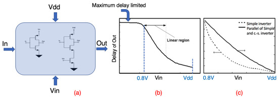
Figure 4.
Schematic of the VCDU presented in [15] (a), with the voltage-delay characteristic (b) and the linearity range (c).
In [16], a Modified Pseudo Differential Current-Starved Delay Element (MPDCSDE) is used to realize a delay cell. The proposed delay cell is shown in Figure 5. Each branch of the delay cell is implemented as a two-stage inverter. All the bulk of the pmos transistor is biased towards Vcp, while the bulk of nmos transistors is biased towards Vcn; the gates of the pmos devices are at Vgp and the gates of the nmos devices are at Vgn, except for the transistors connected to the input or to the output. M1 is the pull-down while M2 is the pull-up transistor. The control voltages Vcn and Vcp, respectively, modulate the ON resistance of the devices M1 and M2. These variable resistances control the current available to the charge or discharge the load capacitance of the first inverter. Moreover, the body bias technique is utilized to widen the applicable range for the controlled signal and improve the linearity. This circuit is powered at 1.5 V and shows a linear behavior for control voltages ranging from 0.2 V to 1.2 V. Therefore, although the linearity range is largely increased, this topology does not show a real rail-to-rail linear characteristic.
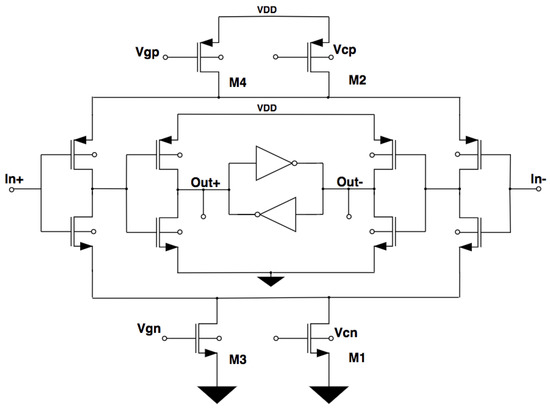
Figure 5.
Schematic of the VCDU presented in [16].
In [17], a VCDU with the extended linear region is also proposed. It is schematically shown in Figure 6.
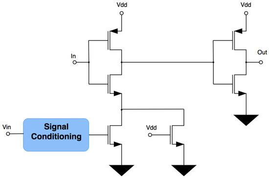
Figure 6.
Schematic of the VCDU presented in [17].
The core of the VCDU is the signal conditioning circuit based on a resistor voltage divider and a mos level shifter. These devices are added to improve the linearity of the VCDU. Without the signal conditioner, indeed, for low-input voltage, the current-starved nmos transistor enters the subthreshold region, causing strong nonlinearity. Overall, the VCDU proposed in [17] has a voltage supply of 1.8 V and a linear range from 0 up to 1.2 V. The VCDU proposed in [18] and shown in Figure 7 is still based on a signal conditioning circuit, but in this case, the circuit is different both in the schematic and in working principle. The conditioning circuit is indeed based on a simple inverting common-source amplifier, with the pmos input device (controlled by Vin) and nmos active load (biased at Vdd); this stage helps in obtaining a quasi-linear monotonic relationship in the delay response of the circuit. However, transistor sizing optimization must be performed by means of a parametric sweep in order to obtain the most linear voltage–delay characteristic: the circuit is therefore simple in the schematic but sensible to process variation.
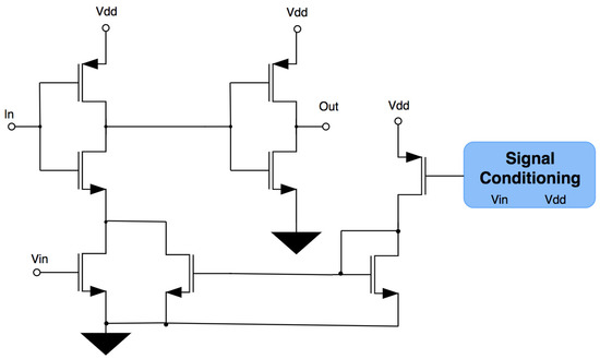
Figure 7.
Schematic of the VCDU presented in [18].
The work presented in [19] is based on the schematic discussed in [18] which is further modified and improved. It is based on a delay element controlled by a voltage Vin on a signal conditioning circuit similar to that depicted in [18] and based on a simple inverting common-source amplifier, with the pmos input device (controlled by Vin) and nmos active load (biased at Vdd) on a balanced current-starved inverter and two switches at the output connected to two capacitors. The latter can provide a rough control of the delay, whereas Vin can precisely tune it. The power supply of the circuit in [19] is 1.8 V and the linear range goes from 0.8 V up to 1.8 V; moreover, thanks to the switchable capacitors, a wider delay range can be obtained. A comparison between the main topologies implemented to increase the linearity range of the delay cell is summarized in Table 1. The comparison is limited to the voltage supply and the linear range, but other parameters should be considered in a practical project, such, for example, the area, the power consumption or the linear distortion. These data are often not available or cannot be directly compared because the various VCDUs are fabricated in different technologies. As shown in the table, it is hard to obtain a rail-to-rail linear range. The architecture based on the conditioning amplifier is the best from this point of view; however, the results show a quasi-linear characteristic very sensible to the process variation.

Table 1.
Comparison between state-of-the-art VCDU.
3. The Proposed VCDU
The proposed VCDU is shown in Figure 8.
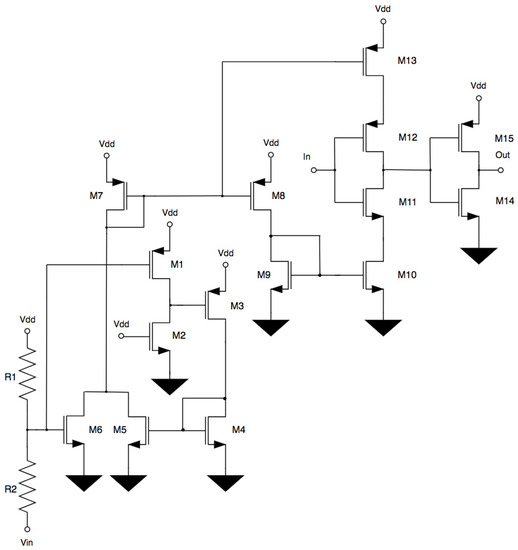
Figure 8.
Schematic of the proposed VCDU.
This was designed with the objective of improving the linearity range and at the same time to increase the flexibility of the delay element. Indeed, in the novel VCDU, the rising and falling transient of the output voltage are symmetrical and the voltage-to-time gain of the cell can be easily modified by means of the components’ sizes. The proposed VCDU is based on the architecture suggested in [18] which has been further modified and improved to achieve a very wide linearity range and a higher robustness against process variations by combining the ideas of the signal conditioning circuit proposed in [17]. The delay of the output (Vout) with respect to the input signal (In) is controlled by a voltage obtained from a resistive voltage divider between the control voltage (Vin) and the power supply (1.8 V), as visible in Figure 8. The voltage divider therefore acts as a level shifter. As such, the control voltage is always higher than the threshold voltage Vtn, preventing the transistor M4-M6 entering the subthreshold region. Indeed, as shown in the literature, when transistors enter the subthreshold region, they cause significant distortion and therefore linearity issues. To this aim, the value of the resistors must be chosen to obtain the proper control voltage. Then, the value of the resistors will be a compromise between power and area consumption. Nevertheless, it is worth adding that a precise value of them is not mandatory because the circuit is not affected by the mismatch of the components. The proposed VCDU was designed in a standard 1.8 V 180 nm CMOS process which is proprietary to the United Microelectronics Corporation (UMC) and the circuit extracted from the layout was deeply simulated and characterized using the Cadence tool named Virtuoso, which is available from the Design Kit. The gain, meaning the delay versus the control voltage, has an absolute value of 82 ps/V. The delay unit exhibits good linearity in the maximum voltage range, which is rail to rail, from 0 to 1.8 V of the control voltage Vin, as shown in Figure 9. This is also evident from the linear regression and from the linearity error, which is less than 10−3 in practically all the rail-to-rail range, as can be seen in Figure 10. The components’ mismatch, temperature variations and changes in the voltage supply Vdd affect the delay characteristic of the proposed VCDU but have a negligible effect on the linearity of the circuit. Several plots of the simulations we ran are attached to show the overall performance of the VCDU (see Figure 11, Figure 12 and Figure 13).
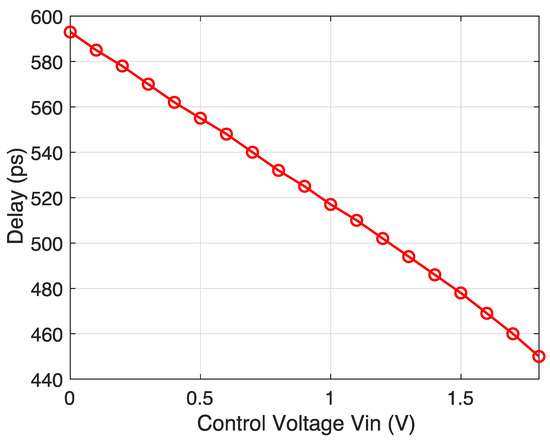
Figure 9.
The delay–Vin characteristic of the proposed VCDU.
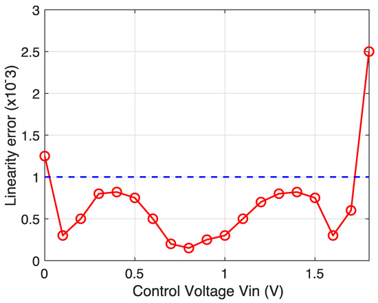
Figure 10.
The linearity error of the proposed VCDU.
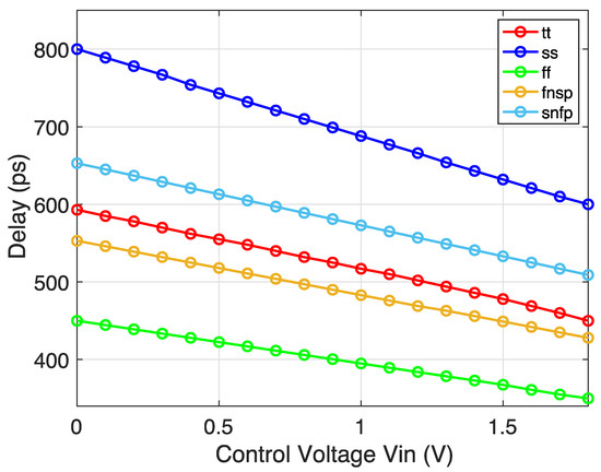
Figure 11.
The delay–Vin characteristic of the proposed VCDU using typical (tt), slow (ss), fast (ff) and fast-n slow-p (fs), slow-n fast-p (sf) transistor models.
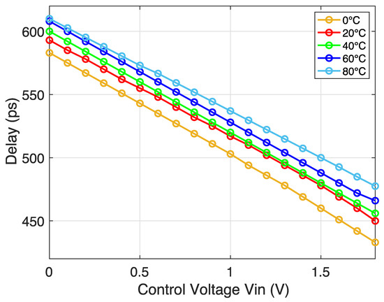
Figure 12.
The delay–Vin characteristic of the proposed VCDU at different temperatures from 0 °C to 80 °C.
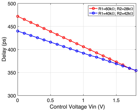
Figure 13.
The delay–Vin characteristic of the proposed VCDU for maximum mismatch between R1 and R2.
Finally, for the sake of completeness, the overall sizing of the circuits is listed in Table 2 and the layout is shown in Figure 14: the area is 37 μm × 65 μm.
Table 2.
Circuit sizing.
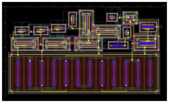
Figure 14.
Layout of the proposed VCDU.
4. EMI
It has recently been demonstrated that the effect of the electromagnetic interferences can affect a generic VCDU as well as the voltage-to-time converter (VTC) based on VCDU [13,14]. The interferences can indeed reach the devices through the I/O pins and they can eventually lead to failures [10,11,12] in a generic-integrated circuit; in the case of time-mode circuits, the interfering signal can cause, in particular, an EMI-induced jitter, as illustrated in Figure 15.
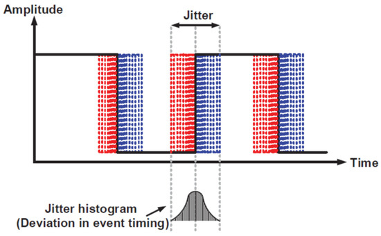
Figure 15.
Jitter on a squared wave signal.
The investigation of the EMI susceptibility in VCDU is therefore interesting and necessary. The first step to characterize the susceptibility of the proposed VCDU is to find the most critical paths. The VCDU, as shown in the schematic of Figure 8, has two input pins (Vin, Vclk) and two pins for the power supply (Vdd and Gnd). Vclk is generated inside the integrated circuit but Vin is external and can pick up the interferences, leading them to the voltage-to-time converter. Moreover, the interferences reaching the pin are critical because this signal cannot be filtered; instead, generally speaking, it is possible to filter the noise from the power supply lines.
To investigate the EMI effect in the proposed VCDU, several (time-consuming) transient simulations are performed on the circuit extracted from the layout using the Cadence tool named Virtuoso, available from the Design Kit. In particular, the control voltage Vin, which is set to 0.9 V DC, is simulated as affected by an 0DC mean value sinusoidal signal with an amplitude ranging from 200 mVp up to 600 mVp and a frequency set at 100 MHz, 500 MHz, 1 GHz and 5 GHz (because several simulations show that the worst case is right between hundreds of MHz until GHz [10,11]). The initial phase of the EMI is swept from 0° to 340° and the average EMI-induced jitter is calculated and plotted in Figure 16 because it is an interesting and important way to quantify the EMI susceptibility of the circuit, as suggested in the most recent literature about this topic [13]. Due to interferences, the delay moves only slightly away from the nominal condition (525 ps, represented by the black solid line in Figure 16) and the proposed VCDU exhibits a small average EMI-induced jitter: this depends on both the EMI amplitude and the frequencies, but it is always limited to approximately 1% of the nominal delay.
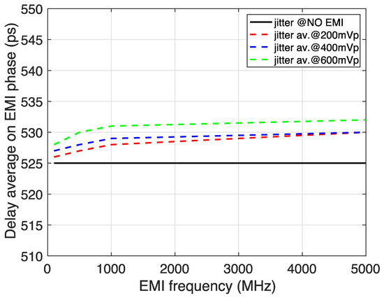
Figure 16.
Average delay @Vin = 0.9 V + EMI.
These results confirm those observed in [13] where the classical current-starved delay unit of Figure 3 with a limited linearity range) is exposed to the interferences and compared to another VCDU with improved linearity. The average EMI-induced jitter of the first topology is 25% of the nominal delay for an EMI amplitude of 200 mV and it increases up to 40% for 600 mV of interference amplitude. The second topology considered in [13] is similar to that of [17], which exhibits a wider linear range (although still not rail to rail) and a lower susceptibility to interferences. Indeed, the average EMI-induced Jitter is approximately 10–20% of the nominal delay. A comparison between these three topologies is summarized in Table 3.
Table 3.
Comparison between the VCDU in terms of linearity and EMI-induced jitter.
5. Conclusions
EMI susceptibility is a critical issue not only in analog integrated circuits but also in digital and mixed ones. Although the EMI compatibility has been deeply investigated in the analog domain, this study is also currently of paramount importance for digital integrated circuits, especially when they are used to implement analog functions, as in the case of digital-based amplifiers and time-mode signal processing. The survey can be devoted to find the possible causes of EMI susceptibility, or the mechanism of the interference propagation, or the most detrimental EMI effects. This field of research is rather novel and few works focused on this topic can be found in the literature. This paper aims to bridge this gap, particularly to help the IC designer find the best solutions to the EMI issue. The final result of this work is evidence of a correlation between the linearity range and the susceptibility to the electromagnetic interferences: it is indeed demonstrated by considering the main state-of-the-art topologies and by comparing their average EMI-induced jitter.
Author Contributions
The authors contributed equally to this work. Conceptualization and methodology were done by A.R., investigation and design were done by F.A.B. and L.C.; original draft preparation was done by A.R.; review and editing was done by F.A.B. and L.C. All authors have read and agreed to the published version of the manuscript.
Funding
This research received no external funding.
Institutional Review Board Statement
Not applicable.
Informed Consent Statement
Not applicable.
Data Availability Statement
Not applicable.
Conflicts of Interest
The authors declare no conflict of interest.
References
- Crovetti, P.; Musolino, F.; Aiello, O.; Toledo, P.; Rubino, R. Breaking the boundaries between analogue and digital. Electron. Lett. 2019, 55, 672–673. [Google Scholar] [CrossRef]
- Coccoli, A.; Richelli, A.; Redouté, J.-M. EMI susceptibility of a digitally based analog amplifier in a 180-nm CMOS process. IEEE Trans. Electromagn. Compat. 2016, 58, 1236–1239. [Google Scholar] [CrossRef]
- Ng, K.A.; Xu, Y.P. A low-power, high CMRR neural amplifier system employing CMOS inverter-based OTAs with CMFB through supply rails. IEEE J. Solid-State Circuits 2016, 51, 724–737. [Google Scholar]
- Crovetti, P. A digital-based analog differential circuit. IEEE Trans. Circuits Syst. I Regul. Pap. 2013, 60, 3107–3116. [Google Scholar] [CrossRef]
- Roberts, G.W.; Ali-Bakhshian, M. A Brief Introduction to Time-to-Digital and Digital-to-Time Converters. IEEE Trans. Circuits Syst. II Express Briefs 2010, 57, 153–157. [Google Scholar] [CrossRef]
- Tancock, S.; Arabul, E.; Dahnoun, N. A Review of New Time-to-Digital Conversion Techniques. IEEE Trans. Instrum. Meas. 2019, 68, 3406–3417. [Google Scholar] [CrossRef]
- Tierno, J.A.; Rylyakov, A.V.; Friedman, D.J. A Wide Power Supply Range, Wide Tuning Range, All Static CMOS All Digital PLL in 65 nm SOI. IEEE J. Solid-State Circuits 2008, 43, 42–51. [Google Scholar] [CrossRef]
- Taillefer, C.S.; Roberts, G.W. Delta-Sigma A/D Conversion via Time-Mode Signal Processing. IEEE Trans. Circuits Syst. Regul. Pap. 2009, 56, 1908–1920. [Google Scholar] [CrossRef]
- Gopal, S.; Agarwal, P.; Baylon, J.; Renaud, L.; Ali, S.N.; Pande, P.P.; Heo, D. A Spatial Multi-Bit Sub-1-V Time-Domain Matrix Multiplier Interface for Approximate Computing in 65-nm CMOS. IEEE J. Emerg. Sel. Top. Circuits Syst. 2018, 8, 506–518. [Google Scholar] [CrossRef]
- Directive IEC 62132. Integrated Circuits, Measurements of Electromagnetic Immunity up to 1 GHz. Available online: www.iec.ch (accessed on 8 February 2022).
- Redouté, J.-M.; Richelli, A. A methodological approach to EMI resistant analog integrated circuit design. IEEE Electromagn. Compat. Mag. 2016, 65, 1369–1379. [Google Scholar] [CrossRef][Green Version]
- Richelli, A.; Delaini, G.; Grassi, M.; Redouté, J.-M. Susceptibility of Operational Amplifiers to Conducted EMI Injected Through the Ground Plane into Their Output Terminal. IEEE Trans. Electromagn. Compat. 2015, 4, 92–100. [Google Scholar] [CrossRef]
- Richelli, A.; Colalongo, L.; Kovács-Vajna, Z.-M. EMI Effect in Voltage-to-Time Converters. IEEE Trans. Circuits Syst. II Express Briefs 2021, 68, 1078–1082. [Google Scholar] [CrossRef]
- Richelli, A.; Colalongo, L.; Kovács-Vajna, Z.M. EMI Effects in CMOS Time-Mode Circuits. In Proceedings of the 2020 International Symposium on Electromagnetic Compatibility-EMC EUROPE, Rome, Italy, 23–25 September 2020; pp. 1–6. [Google Scholar]
- Farkhani, H.; Meymandi-Nejad, M.; Sachdev, M. A fully digital ADC using a new delay element with enhanced linearity. In Proceedings of the 2008 IEEE International Symposium on Circuits and Systems (ISCAS), Seattle, WA, USA, 18–21 May 2008; pp. 2406–2409. [Google Scholar]
- Moazedi, M.; Abrishamifar, A.; Sodagar, A.M. A highly-linear modified pseudo-differential current starved delay element with wide tuning range. In Proceedings of the 2011 19th Iranian Conference on Electrical Engineering, Tehran, Iran, 17–19 May 2011. [Google Scholar]
- Ziabakhsh, S.; Gagnon, G.; Roberts, G.W. Wide linear range voltage-controlled delay unit for time-mode signal processing. In Proceedings of the IEEE International Symposium on Circuits and Systems (ISCAS), Lisbon, Portugal, 24–27 May 2015. [Google Scholar]
- Rivandi, H.; Ebrahimi, S.; Saberi, M. A low-power rail-to-rail input-range linear delay element circuit. AEU-Int. J. Electron. Commun. 2017, 79, 26–32. [Google Scholar] [CrossRef]
- Gauci, J.L.; Gatt, E.; Casha, O.; Cataldo, G.D.; Grech, I.; Micallef, J. Design of a Quasi-Linear Rail-to-Rail Delay Element with an Extended Programmable Range. In Proceedings of the 2018 25th IEEE International Conference on Electronics, Circuits and Systems (ICECS), Bordeaux, France, 9–12 December 2018; pp. 265–268. [Google Scholar]
Publisher’s Note: MDPI stays neutral with regard to jurisdictional claims in published maps and institutional affiliations. |
© 2022 by the authors. Licensee MDPI, Basel, Switzerland. This article is an open access article distributed under the terms and conditions of the Creative Commons Attribution (CC BY) license (https://creativecommons.org/licenses/by/4.0/).