Abstract
This paper traces the history of the evolution of inverse analog filters (IAF) and presents a review of the progress made in this area to date. The paper, thus, presents the current state-of-the art of IAFs by providing an appraisal of a variety of realizations of IAFs using commercially available active building blocks (ABB), such as operational amplifiers (Op-amp), operational transconductance amplifiers (OTA), current conveyors (CC) and current feedback operational amplifiers (CFOA) as well as those realized with newer active building blocks of more recent origin, such as operational transresistance amplifiers (OTRA), current differencing buffered amplifiers (CDBA) and variants of current conveyors which, although not available as off-the-shelf ICs yet, can be implemented as complementary metal–oxide–semiconductors (CMOS) or be realized in discrete form using other commercially available integrated circuits (IC). In the end, some issues related to IAFs have been highlighted which need further investigation.
1. Introduction
Over the last twenty-five years, there has been considerable interest and research effort in the technical literature on the circuit realizations of inverse analog filters. In many areas such as communication, control and instrumentation, inverse filters may be required to correct the distortions of the signals caused by the signal processors. Since inverse filters have a frequency response which is reciprocal of the frequency response of the system which caused the distortions, it is expected that this can be corrected by using an inverse filter. A survey of the work done on the realization of inverse filters indicates that before the publication of the 1997 paper of Adrian Leuciuc [1], although there had been mention of digital inverse filters from time-to-time [2,3,4,5,6], only the 1964 paper of Burch, Green and Grote [6] had discussed earlier about the restoration and correction of time functions by the synthesis of inverse filters on analog computers. Thus, with the sole exception of [6] and before the 1997 work of Leuciuc [1], no procedure or circuit appears to have been presented in the open technical literature to realize any kind of inverse analog filters using the now prevalent analog circuit building blocks.
However, subsequent to the publication of [1], a number of authors have come up with various kinds of circuits for realizing IAFs [7,8,9,10,11,12,13,14,15,16,17,18,19,20,21,22,23,24,25,26,27,28,29,30,31,32,33,34,35,36,37,38,39,40,41,42,43] using a variety of active building blocks such as the four-terminal floating nullors (FTFN) [44,45], operational transconductance amplifiers (OTA) [46], current conveyors [47,48] and their many variants such as differential difference current conveyors (DDCC), second generation voltage conveyors (VCII), current feedback operational amplifiers (CFOA) [49], operational transresistance amplifiers (OTRA) [50], current differencing buffered amplifiers (CDBA) [51], current differencing transconductance amplifiers (CDTA) [52], voltage differencing transconductance amplifiers (VDTA) [53], etc. This paper gives an account of the progress made on the evolution of IAFs so far and points out some unresolved problems and issues related to them.
2. The Transfer Functions of Inverse Filters, Their Frequency Responses, the Significance of the Various Parameters and the Stability Issues
In this section, we discuss the frequency response of the various types of inverse filters, and attempt to provide the significance of the various parameters H0, ω0 and Q0 on the shape of the frequency responses. We also comment upon the stability issues related to the various types of inverse filters.
2.1. Significance of the Coefficients of the Inverse Transfer Functions in the Characterization of Their Frequency Responses
The physical meaning of the parameters H0, Q0 and ω0 is clear in the context of normal low-pass (LP) and high-pass (HP) filters, and that of H0, ω0/Q0 (BW) and ω0 is also clear in the case of normal band-pass (BP) and band reject (BR) filters. However, so far, the significance of the various coefficients of the inverse transfer functions and their influence on the shapes of the corresponding frequency responses does not appear to have been elaborated explicitly in the earlier literature. In the following, we attempt to provide some insight into this.
Let us consider an inverse low pass filter (ILPF) transfer function, which can be written as:
From this transfer function, it can be verified that |T(jω)| at zero frequency (DC) turns out to be 1/H0; at ω = ∞, |T(jω)| becomes ∞, and at a frequency ω = ω0, |T(jω)| is given by:
Therefore, ‘ω0’ can be called the corner frequency; however, depending upon whether Q0 = 1, Q0 > 1 or Q0 < 1, the resulting responses turn out to be as shown in Figure 1.
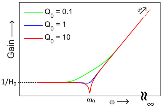
Figure 1.
Frequency responses of ILPF for different values of Q0.
Hence, the significance of the coefficients H0, Q0 and ω0 is clear from this plot.
In a similar manner, the transfer function of inverse high pass filter (IHPF) may be expressed as:
For the IHPF, |T(jω)| at ω = 0 turns out to be ∞; at ω = ∞, |T(jω)| becomes 0 and at a frequency ω = ω0, |T(jω)| is given by:
Therefore, in the case of IHPF also, ω0 is the corner frequency and depending upon whether Q0 = 1, Q0 > 1 or Q0 less than 1, the resulting responses would be as displayed in Figure 2.
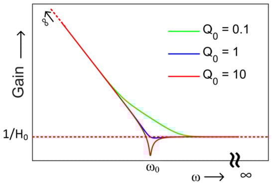
Figure 2.
Frequency responses of IHPF for different values of Q0.
The transfer function of inverse band pass filter (IBPF) may be expressed as:
The |T(jω)|IBPF can be written as:
From Equation (6), it may be seen that, for ω = 0 and ω = ∞ in both cases, |T(jω)| is infinite and at ω = ω0, |T(jω| turns out to be 1/H0. The frequency response for IBPF has been shown in Figure 3a. Here, ω0 is the center frequency.
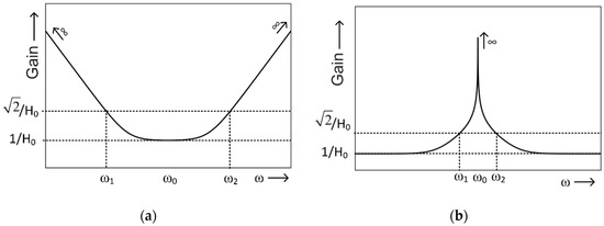
Figure 3.
Frequency response of (a) IBPF and (b) IBRF.
The transfer function of the IBRF can be written as:
The magnitude of the function in Equation (7) at s = jω can be written as:
From Equation (8), it can be seen that |T(jω)| of the notch filter at ω = 0 as well as ω = ∞, is 1/H0 whereas, at ω = ω0, |T(jω)| tends to infinity. Here also, ω0 is the center frequency and the shape of response is as shown in Figure 3b.
In case of IBPF as well as IBRF, a narrowing down (sharpness) of the shape of the frequency response is observed when Q0 is increased. For a quantitative interpretation of this, if we take ω0 = 1 (normalized value) and determine the two frequencies (ω1 and ω2), on either side of the center frequency, at which the gain becomes (arbitrarily chosen to facilitate easy solution of the resulting quadratic equation) can be found from Equations (6) and (8) and turn out to be:
from which it can be seen that the width of the IBP and IBR plots between these two frequencies is given by:
From Equation (9), it is clear that, the larger the value of Q0, the narrower the width of the resulting frequency response at the gain value of , which is clearly visible from the plots of Figure 4a,b. On the contrary, for values of Q0 < 1, the nature of the plot would be wider on either side of ω0. The frequency responses of IBPF and IBRF for different values of Q0 shown in Figure 4a,b confirm this interpretation.
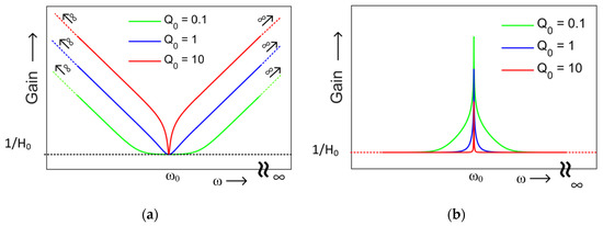
Figure 4.
Frequency responses of (a) IBPF and (b) IBRF for different values of Q0.
Lastly, we do not deal with inverse all-pass filters (IAPF), since in our opinion, IAPF is a misnomer due to being an unstable system owing to having complex conjugate poles in the right half of the s-plane.
2.2. Stability Considerations
On the stability of inverse analog filters: Another potential problem which does not appear to have been noticed explicitly in the existing literature is concerned with the stability aspect of inverse filters. In case of the first order inverse filters, the ILP and IHP do not have stability issues; however, the inverse all pass filter transfer function clearly has its pole in the right half of the s-plane and, therefore, represents an unstable system. Coming to second order inverse filters, ILP and IBP do not have stability problems, but in the case of IHP, there is pair of poles at its origin, the IBR has a pair of poles on the ±jω axis and the inverse all pass (IAP) has clearly both poles in the right half of the s-plane. Thus, theoretically, all these cases represent unstable systems. Now, the fact that a number of authors have come up with first-order inverse all-pass filter [10,19,33], second order IHP [1,9,11,12,13,14,15,16,17,18,20,22,23,27,28,30,32,35,36,39,40,41,42,43], IBR [11,12,15,17,22,24,25,27,29,32,35,36] and IAP [8,9,24,27,29] filters, it is a matter of curiosity as to how the observance of instability was not reported by any of them. There could be two possible reasons for this:
- (i)
- As is well known, if the verification of the workability of the circuit is carried out only by frequency response analysis in SPICE without checking the transient response of the circuits, they may still exhibit the correct frequency responses and, thus, the circuit instability might go unnoticed in the absence of looking into its transient analysis.
- (ii)
- In those cases where experimental results of the frequency responses of such circuits are taken and the circuits are shown to work properly, the possible reason could be that the various parasitics of the active element used or their non-ideal parameters might have shifted the pole locations slightly to the left half of the s-plane (which appear feasible in case of IHP or IBR but unlikely in the case of inverse all-pass filters) and therefore, any instability could not have been observed.
- (iii)
- Of course, a stability issue of fractional order inverse filters (FOIFs) together with a check of their transient response is similarly necessary. In fact, Bhaskar et al. in [40] and Radwan et al. [41] have already taken due cognizance of this aspect.
Thus, the stability issues related to the IHP, IBR and IAP call for further investigations in future.
3. Circuit Realizations of the Various Inverse Analog Filters
In this section, we outline some prominent inverse analog filter configurations using different kinds of analog circuit building blocks proposed during the last two decades or more.
3.1. IAF Configurations Using Op-Amps and FTFNs
Leuciuc [1] appears to be the first to have presented a general methodology of finding the inverse of a given analog circuit based upon the use of nullator and norator which are two well-known pathological elements proposed by Carlin and Youla [54]. It may be recalled that the nullator is a one port (two-terminal element) characterized by the equations V = 0, and I = 0; on the other hand, the norator is another one port (two-terminal element) characterized by V = arbitrary and I = arbitrary. The methodology proposed by Leuciuc [1] is depicted in Figure 5, according to which a network ‘N’ containing a nullator and norator and realizing a transfer function Y(s)/U(s) = T(s) will be converted into another network realizing the transfer function T(s)−1 if the driving source and norator are swapped.
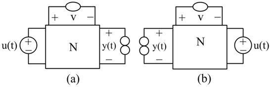
Figure 5.
Original circuit and its inverse obtained by swapping the driving source and the norator (a) original circuit (b) Inverse circuit.
Since a pair of a nullator and a norator (with one end of the norator connected to ground) represents an ideal op-amp [55], this idea is readily applicable in obtaining inverse of any given op-amp filter. Leuciuc [1], using this idea, demonstrated how the well-known single op-amp-based Sallen-Key high-pass filter can be used to realize an inverse high-pass filter as shown here in Figure 6.
Figure 6.
Sallen-Key high pass filter and its inverse by Leuciuc [1] (a) original filter (b) inverse filter.
It is interesting to point out that the transformation of an op-amp circuit realizing a transfer function T(s) into another op-amp circuit realizing transfer function T(s)−1 can also be related to the inverse active network theorem (IANT) proposed by Rathore in [56] and Rathore and Singhi in [57]. As per IANT, if there is an op-amp RC network ‘N’ realizing a transfer function T(s), then this can be transformed into a network realizing the reciprocal transfer function 1/T(s) by bringing the connection of all elements going to the input signal to the output of the op-amp and connecting all elements connected to the output node to the input terminal, then assigning the correct polarities of the input terminals of the op-amp from the considerations of the stability of the resulting circuit. The circuit in Figure 6b can be considered to be obtainable from that of Figure 6a using IANT. Since Leuciuc did not demonstrate the practical results of his inverse filter of Figure 6b starting from zero frequency, it went unnoticed that this circuit cannot be functional because of the absence of a DC path in the negative feedback circuit.
In [37], a number of single-op-amp-based inverse filter circuits have been discussed.
3.2. IAF Configurations Using Four-Terminal-Floating-Nullors (FTFN)
This was followed by another procedure reported by Chipipop and Surakampontorn in [7] for the systematic realization of a current-mode four-terminal floating nullor (FTFN)-based inverse filter as shown in Figure 7 (the acronym ‘FTFN’ to represent a fully floating nullor was coined for the first time in [44,45]). In this procedure, starting from an op-amp circuit, a nullor-RC model is obtained by replacing the ideal op-amp with a pair of a nullator and norator (having one terminal connected to ground). Subsequently, the driving source and norator are swapped as per the transformations suggested by Leuciuc [1] to obtain an inverse filter in voltage mode. This is followed by an RC:CR duality transformation [58] from which an FTFN-based inverse filter in current-mode is obtained, which is converted into a physical realization by replacing the nullator and norator pair by an FTFN. In the work of Chipipop and Surakampontorn [7] the FTFN was realized using an operational-mirrored amplifier (OMA) formulation [59] using AD704 IC op-amp, Q2N2222A NPN transistors and Q2N2907A PNP transistors. Since the FTFN used for the simulation results does not have symmetrical/identical W and Z terminals, the simulation results given in [7] do not ensure that the derived inverse filter will still work satisfactorily in practice when the FTFN is realized by symmetrical structures such as those made from two CCII± or two CFOAs.
Figure 7.
The procedure for realization of FTFN-based inverse filter in CM [7] (a) a single-op-amp filter (b) nullor equivalent (c) inverse function realization in voltage mode (VM) by swapping the voltage source by norator (d) the RC:CR dual to realize the same function in CM as a current-ration transfer function (e) the FTFN implementation of the inverse filter.
Wang and Lee [8] extended this approach and derived a current-mode IAF using FTFN corresponding to the Friend and Delyiannis [60] op-amp-RC biquad and also demonstrated how the same methodology can be applied to derive an FTFN-based current mode inverse filter starting from a CCII-based VM filter, since a CCII- can also be represented by a three-terminal nullor (with the nullator and norator sharing a common terminal which represents the X-terminal of the CCII-, while the free end of the nullator represents the Y-terminal of the CCII- and the free end of the norator represents the terminal-Z). Wang and Lee in [8] have also shown the transformation of a high-input impedance filter into a current-mode inverse filter. In both cases, the verification of the workability of the circuits was demonstrated by only SPICE simulation results although it was not clarified as to which FTFN implementation was used.
Taking clues from the above mentioned FTFN-based approach, Abuelma’atti in [9] formulated a generalized single-FTFN network for realizing a CM transformation using as many as eleven admittances in the circuit and worked out a number of second-order inverse filters in CM as special cases therefrom. The simulation results of these inverse filters were obtained using two-CCII-based realization of the FTFN which was acknowledged in [9] to have been first outlined by Senani in [45], which is shown here in Figure 8. All the circuits employ a low number of passive components and their workability has also been demonstrated by a symmetrical FTFN structure; however, some of the circuits derived therein suffer from the drawback of being non-canonic.
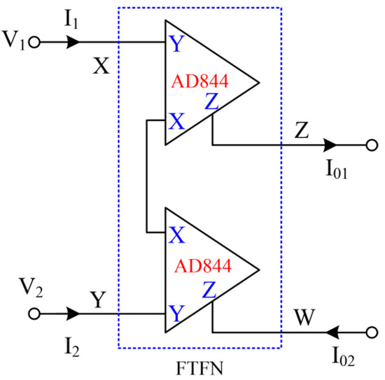
Figure 8.
FTFN realization using two CCIIs [9,45].
Shah and Malik [10] proposed an all-pass inverse filter configuration with two inputs and a single output wherein the FTFN was again implemented using the two-AD844-based implementation, shown here in Figure 8. However, the authors have failed to notice that the first order IAP clearly has the pole located in the right half of the s-plane, and therefore, any circuit implementation of this will be unstable. Therefore, it would fail in the transient response test even though it might show correct frequency response in simulations.
3.3. IAF Configurations Using Current Feedback Operational Amplifiers (CFOA)
A CFOA is a four terminal (x, y, z and w) active building blocks characterized by the following terminal equations:
iy = 0, vx = vy, iz = ix and vw = vz
Since there has been considerable interest in the use of CFOAs as active building blocks because of their several advantages over the traditional voltage mode op-amps (VOA), such as very high slew rates leading to a higher operational frequency range, elimination of the gain–bandwidth conflict and the feasibility of realizing any given function with the least possible number of passive components, most of the time, without requiring any component-matching conditions/equality constraints [49,61,62,63,64,65]. Due to these reasons, a number of researchers have formulated various kinds of IAF circuits too, using CFOAs.
In this context, Gupta, Bhaskar, Senani and Singh [11] were the first to have proposed four inverse filter configurations, each implementable from only three CFOAs for realizing inverse low-pass, inverse band-pass, inverse high-pass and inverse band reject filters respectively. These realizations have been depicted here in Figure 9. The practically observed frequency responses of these circuits were also shown in [11]. All the circuits possessed the important and practically useful properties of infinite input impedance, zero output impedance and the use of two grounded capacitors as preferred for IC implementation [66,67,68,69]. The inverse low pass and band pass filters of Figure 9a,b have the novel feature of having all four resistors being grounded too, which is attractive for IC implementation as well as converting the circuits into voltage-controlled circuits by replacing the grounded resistors with FET/MOSFET-based linear voltage-controlled resistances.
Figure 9.
Proposed inverse filter configurations reported by Gupta, Bhaskar, Senani and Singh using CFOAs (a) ILP (b) IBP (c) IHP (d) IBR [11].
In [12], Gupta, Bhaskar and Senani further extended their work by presenting one new implementation of the IHP filter, four new circuits of the ILP filter and two new configurations of the IBP filter, each employing three CFOAs, two grounded capacitors and three to five resistors along with the provision of independent controllability of the various coefficients of the realized transfer functions. These reported circuits have also been experimentally verified using AD844 type CFOA ICs in the frequency range of 100 Hz–1 MHz.
Subsequently, Wang, Chang, Yang and Tsai [13] proposed a general inverse filter scheme using CFOAs as shown in Figure 10. Curiously, however, the authors of [13] did cite the quoted work as a reference in their paper, but while projecting their general scheme of Figure 10, they did not spell it out explicitly that their configuration is, in fact, an adaptation of the two circuits of Figure 9a,b. It was demonstrated by them that, subject to appropriate (resistive/capacitive) choices of the various circuit admittances, this general circuit can realize twelve different types of inverse filter functions at each of the two outputs V01 and V02. However, out of the twelve realized circuits shown by them, only three circuits represent canonic realizations; the other configurations employ three to four capacitors, and hence, are non-canonic.
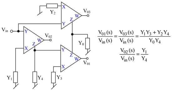
Figure 10.
Generalized inverse filter configuration using CFOAs reported by Wang, Chang, Yang and Tsai [13].
Garg, Bhagat and Jaint [14] presented a general inverse filter scheme which is also an adaptation of the quoted circuits from Figure 9a,b, the only difference being that instead of the three normal CFOAs, three modified CFOAs (MCFOA), characterized by iz = α1ix, iy = α2iw, vx = β1vy, and vw = β2vz [70,71] have been employed, each one implementable from three AD844-type CFOAs or a cascade of one CCII+ and one CCII−. It may, however, be noted [65] that the MCFOA is the same as the ‘Composite Current Conveyor’ formulated by Smith and Sedra in [72] which was comprised of one CCII+ (now realizable with one AD844-type CFOA) and one CCII− (now realizable with two AD844-type CFOAs) to realize various nonlinear circuit elements. For the verification of the workability of these inverse filters, a CMOS MCFOA has been used within the frequency range of 1 kHz–1 GHz. However, all the realized filters used three or more capacitors and hence, are not canonic. Moreover, the ABB used is not available as a commercial IC and needed to be implemented with three AD844s thereby, the proposed configuration requiring as many as nine CFOAs.
Patil and Sharma [15] presented four two-CFOA-based configurations for realizing ILP, IHP, IBP and IBR filters (the last one being inspired by [69]). All these reported circuits have been verified by simulation results in PSPICE using a macro model of AD844. Four of the five circuits have the advantage of being realizable with two only CFOAs. The configurations presented can also provide explicit current output, but at the expense of one additional CFOA.
3.4. IAF Configurations Using Operational Transconductance Amplifiers (OTA)
The OTA is characterized by I0 = gm (V+ − V−) and has been extensively used in the past to realize electronically controllable filters and oscillators. The bipolar OTA is also a commercially available device and many variants of this such as LM3080, LM13600/LM13700 are available as off-the-shelf ICs whose transconductance is a linear function of an external DC bias current (IB) and is linearly variable over a wide range of this current up to about four decades. On the other hand, a CMOS OTA as shown in Figure 11 can be analogously devised using a MOS differential pair along with a number of PMOS/NMOS current mirrors. However, for the CMOS OTA, the transconductance is proportional to (IB)1/2. CMOS OTAs with dual outputs, such as the one shown in Figure 11, have been employed by several authors [16,17].
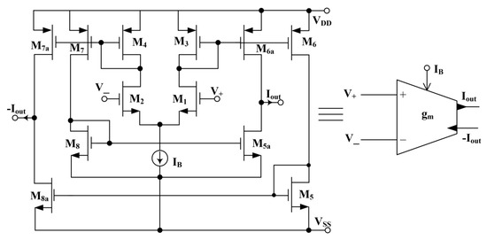
Figure 11.
CMOS implementation and symbolic representation of the dual-output OTA.
In [16], Tsukutani, Sumi and Yabuki presented two six-OTA-based circuits, realizing ILP and IBP, and one five-OTA-based circuit realizing IHP as depicted here in Figure 12. All the circuits employ both GCs and have the advantage of offering orthogonal tunability of the parameters ω0 and Q0 which has been successfully demonstrated by SPICE simulation results. The workability of inverse filter circuits shown in Figure 12 has been validated over a frequency range of 10 kHz–1 MHz using CMOS OTA displayed in Figure 11. However, if the circuits are implemented using commercially available IC OTAs, the actual number of IC OTAs required may be more in each case.
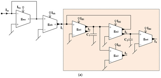
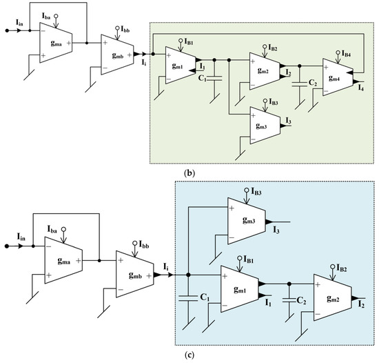
Figure 12.
The basic current-mode inverse active filter configurations proposed by Tsukutani, Sumi and Yabuki in [16]. (a) ILPF; (b) IBPF; (c) IHPF.
The transfer functions of the IAFs shown in Figure 12 have been presented here:
| Figure 12a ILPF | |
| Figure 12b IBPF | |
| Figure 12c IHPF |
In [17], Raj, Bhagat, Kumar and Bhaskar presented five new OTA-C inverse filters which include one IHP, two ILP, one IBP and one IBR, all possessing infinite input impedance and employment of both grounded capacitors, with ω0 and Q0 being orthogonally adjustable. Their workability was demonstrated by a simple CMOS OTA with its gm controllable by an external DC bias voltage.
3.5. IAF Configurations Using Second Generation Current Conveyors (CCII)
It may be recalled that a CCII± is a three-port active building block [47,48] characterized by iy = 0, vx = vy and iz = ±ix. Tsukutani and Kunugasa [18] have proposed three different configurations which simultaneously realize current mode ILP, IBP and IHP filters (Figure 13); two of them employ four current conveyors, while the third one employs only three CCIIs. However, whereas the first two circuits realize only ILP and IBP functions, the third one realizes only IHP response. Although it is not explicitly stated by the authors, these CCII-based circuits are derived directly from the OTA-C IAF circuits of [16], with each transconductor therein replaced by a CCII- based V-I convertor with a resistor connected from the X-terminal of the CCII to ground. All the circuits use all grounded passive components and the CCII involved was a standard translinear CMOS structure with two complementary Z-outputs (see Figure 14). To validate the functionality of these inverse filters, CMOS CCII, shown in Figure 14, has been used and the results showed the workability of these circuits in the frequency range of 10 kHz–10 MHz.
Figure 13.
Current-mode inverse active configurations by Tsukutani and Kunugasa [18] (a) ILP (b) IBP (c) IHP.
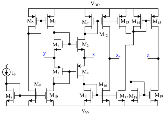
Figure 14.
CMOS implementation of the CCII as employed in [18].
In spite of the advantage of all grounded passive elements, although the proposed circuits do have a high output impedance output available, none of them are able to provide the required (ideally zero) input resistance necessary for applying a CM input. The authors have also indicated that by adding a voltage to current converter (V-I) at the input and a resistive load along with a voltage follower at the output, all three CM IAFs can be converted into VM IAF circuits. These additional interfacing circuits too have been proposed to be realized by one CCII each.
A first order inverse all-pass filter using a single CCII- has been reported by Shah and Rather in [19], wherein the CCII- was implemented using two CCIIs+. However, the circuit clearly has a pole in the right half of the s-plane, and hence, is impractical due to being unstable.
In [20], Herencsar, Lahiri, Koton and Vrba have reported three new realizations of the inverse filters low-pass filter, inverse band-pass filter, and inverse high-pass filter employing differential difference current conveyors (DDCCs) [73], two grounded resistors and two grounded capacitors. It may be recalled that a DDCC is a five-terminal (x, y1, y2, y3 and z) active building block characterized by iyi = 0, i→1–3, vx = vy1 – vy2 + vy3 and iz = ±ix. The reported inverse filter circuits have been validated using SPICE simulations and experimental measurements [20].
3.6. IAF Configurations Using Second Generation Voltage Conveyors (VCII)
An interesting variant of the CCII is the so-called second-generation voltage conveyor (VCII) [74] which is characterized by the equations: ix = ±βiy, Vz = αVx and Vy = 0, where nominally, α and β are both unity. The use of VCII in realizing IAFs has been carried out by Al-Absi in [21] and Al-Shahrani and Al-Absi in [22]. The circuits proposed in both the papers are based around a CMOS implementation of the VCII as displayed in Figure 15 here, which has been claimed to offer the advantages of lower power consumption and less occupied chip area.
Figure 15.
CMOS implementation of the VCII [75].
In [21], Al-Absi proposed two VCII-based circuits for realizing first order ILP and IHP and three-VCII-based circuit for realizing IBP; these are shown in Figure 16. Though all the circuits provide the desirable low-output impedance voltage output, none of them has ideally infinite input impedance.
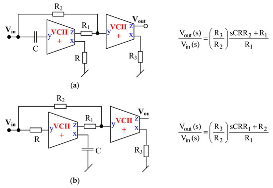
Figure 16.
VCII-based inverse filters reported by Al-Absi (a) ILP (b) IHP and (c) IBP [21].
A claimed advantage of these circuits is that control of H0 and ω0 is available in the cases of ILP, IHP and IBP. The workability of these reported circuits has been verified by simulation results using CMOS VCII, shown in Figure 15, and their frequencies of operation were taken in the range of 1 Hz to 10 MHz.
This was followed by Al-Shahrani and Al-Absi in [22], wherein a modified-VCII (MVCII) proposed earlier in [75] was employed, which is characterized by the following equations:
Iy1 = ±βiy, Ix = βiy, Vz = αVx, Vy = 0 and iz0 = iz
Using MVCII, the authors of [22] presented four CM circuits realizing ILP, IHP, IBR and IBP respectively, using only two external resistors and two capacitors in each case. The IBR and IBP have the advantage of using both GCs, but due to being two-resistor and two-capacitor structures; they do not provide independent tunability of the various filter parameters. For the workability of these circuits, frequency and time responses using CMOS MVCII have been demonstrated.
3.7. IAF Configurations Using Operational Transresistance Amplifiers (OTRA) and Current Differencing Buffered Amplifiers (CDBA)
To overcome the limitations of the conventional op-amp, researchers had been continuously coming up with new active circuit building blocks which resulted in the evolution of several alternatives, of which OTAs, CCs, CFOAs are now available as off-the-shelf ICs. However, there are a number of other building blocks such as OTRA and CDBA, which have been investigated for their hardware implementation and applications in the past. Although both of these can be implemented by CMOS circuits, none of them have yet been made available as off-the-shelf ICs. Nevertheless, both of them can be realized using two commercially available AD844-type CFOAs.
An OTRA is characterized by: vp = vn = 0 and v0 = Rm (ip − in) and is shown symbolically in Figure 17.
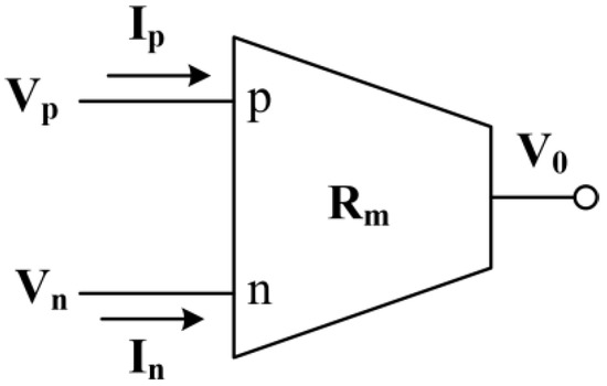
Figure 17.
The symbolic representation of an OTRA.
On the other hand, CDBA is characterized by the terminal equations as: Vp = Vn = 0, Iz = (Ip − In) and Vw = Vz and its symbolic representation is depicted in Figure 18.
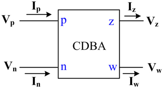
Figure 18.
The symbolic representation of the CDBA.
Both of these are realizable from interconnection of two CFOAs as shown in Figure 19. In case of the CDBA implementation, if a load impedance is connected at terminal-Z, the voltage across this (Vz) is then made available as Vw = Vz. On the other hand, for OTRA implementation, this load impedance connected at terminal-Z becomes the transresistance Rm and for making Rm = ∞ as desired; this terminal, therefore, needs to be left open.
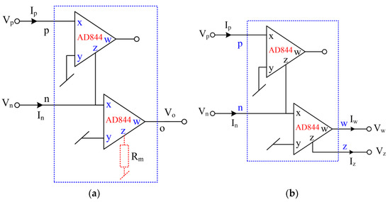
Figure 19.
AD844 implementation of (a) OTRA (Rm = ∞) (b) CDBA.
In the following, we outline some of the prominent works dealing with the realization of inverse filters using CDBA and OTRA.
3.7.1. OTRA-Based Inverse Active Filters
In [23], Singh, Gupta and Senani proposed two OTRA and five admittance-based general inverse filter structures shown in Figure 20, from which an ILP, IBP and IHP, were shown to be realizable in VM via appropriate (resistive/capacitive) choice of the five circuit admittances. Although the IHP was non-canonic due to the employment of three capacitors along with equality constraints, the remaining two realizations are canonic in terms of capacitors and have the advantage of independent controllability of the various filter parameters. For the verification of the workability of the filter functions, PSPICE results using CMOS OTRA have been provided and experimental results have also been demonstrated using OTRA implemented with commercially available AD844-type CFOAs, as shown in Figure 19a.
Figure 20.
A generalized OTRA-based structure for realizing inverse filters proposed by Singh, Gupta and Senani [23].
The configurations reported by Pradhan and Sharma in [24] were generalized by providing two different configurations adding two more admittances in the two-OTRA-based configurations of [23] as shown in Figure 21. The authors then came up with the generation of ten different second-order IBR filters and twelve inverse all-pass (IAP) filter circuits by making various resistive/capacitive choices of the seven admittances therein.
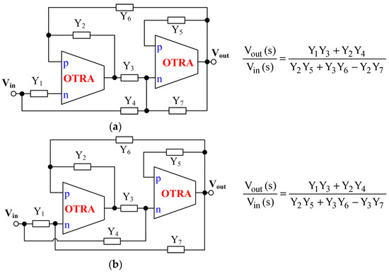
Figure 21.
Generalized configuration of IBR and inverse all-pass filter employing OTRAs proposed by Pradhan and Sharma (a) IBRF (b) IAPF [24].
However, all the special cases required three to four capacitors and, hence, are non-canonic. Various simulation results using CMOS OTRA implemented with 0.18 µm TSMC technology parameters have been provided to validate the workability of all the reported cases of IBRF and IAPF over the frequency range 1 kHz–10 MHz. However, since most of the results were verified through simulations, the inherent stability of IAPF appears to have gone unnoticed.
Banergee, Borah, Ghosh and Mondal in [25] have come up with a configuration using a single OTRA, but the circuit requires as many as three resistors and three capacitors along with three switches to realize band reject filters; hence, these circuits too are non-canonic. Simulations as well as experimental results have been provided for the validation of the proposed circuits. The layout of these three configurations has also been demonstrated and their post-layout simulation results have been provided. The major drawbacks of these circuits are their non-canonicity, non-availability of ideally infinite input impedance and the inconvenience of obtaining different responses through three switches therein.
3.7.2. Inverse Active Filters Employing CDBA
In [27], Pandey, Pandey, Negi and Garg proposed a CDBA-based universal inverse filter circuit consisting of six admittances whose circuit realization has been shown in Figure 22, from which various special cases have been obtained by appropriate RC impedances in place of six admittances of the circuit. However, excepting the circuit for realizing an ILP, which is canonic, all other choices lead to non-canonic structures. A PSPICE macro model of CFOA AD844 IC has been used to implement CDBA (shown in Figure 19b) and the same has been used to verify the workability of the various inverse filter functions.
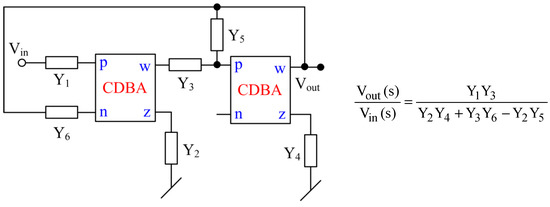
Figure 22.
CDBA-based multifunction inverse filter configuration reported by Pandey, Pandey, Negi and Garg [27].
Nasir and Ahmad in [28] presented a two-CDBA-based CM multifunction inverse filter, but the circuit suffers from the drawback of non-availability of explicit current output, besides one of the input terminals of the CDBA being left unutilized. The CDBA implemented using AD844 shown in Figure 19b has been used to validate the functionality of these inverse filter functions in the frequency range of 10 kHz–1 MHz.
IBR and IAP filters employing two CDBAs were presented in [29] by Bhagat, Bhaskar and Kumar; these filters are based on the general configuration shown here in Figure 23, in which two different responses were obtainable by appropriate opening/closing of a switch from the same output. The circuit uses a GC and another virtually grounded capacitor. In spite of requiring an equality of two resistors, both ω0 and BW can be tuned independently of each other. The workability of this proposition was demonstrated by PSPICE simulations using CMOS CDBA with 0.18 µm CMOS technology parameters. However, there may be stability issues when the circuits are practically realized with CDBA implementation using two CFOA ICs.
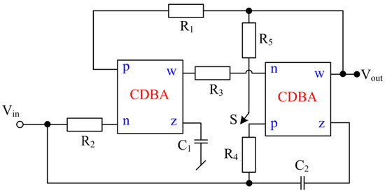
Figure 23.
CDBA-based general configuration for realizing IBR and inverse all-pass filters presented by Bhagat, Bhaskar and Kumar [29].
In [30], Bhagat, Bhaskar and Kumar proposed a two CDBA and four impedances-based circuit from which various inverse filters were shown to be realizable by appropriate resistive/capacitive choice of the various circuit elements. The notable feature of this circuit is that, from the same circuit, both normal filters and inverse filters are realizable with a canonic number of capacitors in all cases. The details of the twelve possible realizations resulting from the circuit of Figure 24 can be seen in [30]. The PSPICE simulation results of these normal filters and inverse filters using CMOS CDBA implemented with 0.18 µm CMOS technology parameters have been provided over the frequency range 10 kHz–50 MHz.
Figure 24.
A multifunction filter/inverse filter configuration employing CDBAs reported by Bhagat, Bhaskar and Kumar [30].
Whereas most of the work has been focused on second-order inverse filters of various kinds, Borah, Singh and Ghosh in [31] have given a realization of a sixth-order inverse band-pass filter. The circuit consists of two CDBAs and eight impedances, which has been practically realized from four AD844-type CFOAs but employs nine capacitors and as many resistors. For the validation of the proposed IBP filter function, experimental results using CDBA implemented with AD844 have been taken and the layout of the proposed configuration has also been provided along with post-layout simulation results. The employment of more (nine) capacitors than really necessary, with most of them being floating, appears to be a clear disadvantage from the viewpoint of actual IC implementation.
While most of the works described above require two CDBAs, a single-CDBA-based inverse filter structure was proposed in [32] by Paul, Roy and Pal. However, out of the four types of filters realizable (ILP, IBP, IHP, IBR), only the ILP is realizable canonically; all others require three capacitors and, hence, are non-canonic. The various inverse filter functions have been validated using CMOS CDBA as well as CDBA implemented with AD844-type CFOAs.
3.8. Inverse Active Filters Employing Current-Differencing Transconductance Amplifier (CDTA)
The CDTA introduced by Biolek [52] is an active building block characterized by vp = vn = 0, iz = ip − in and ix± = ±gmvz, symbolically represented as in Figure 25.
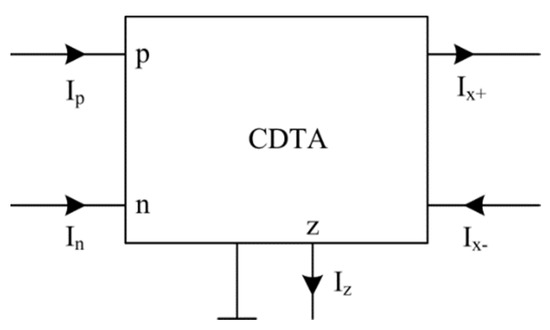
Figure 25.
The symbolic representation of the CDTA [52].
A single-CDTA-based first order inverse all-pass filter was presented in [33] by Shah, Quadri and Iqbal. However, the authors have failed to notice the instability because of the verification through only SPICE simulations and that too, without checking the transient response.
In [34], Sharma, Kumar and Whig proposed a three-CDTA-based IHPF whose circuit configuration has been displayed in Figure 26.
Figure 26.
CDTA based inverse high-pass filter configuration reported by Sharma, Kumar and Whig [34].
The workability of the reported circuit has been verified in PSPICE using CMOS CDTA with 0.35 µm CMOS technology parameters and the frequency responses have been demonstrated in the range of 1 Hz–100 MHz. The circuit suffers from the drawback of neither having infinite input impedance nor low output impedance.
3.9. Inverse Active Filters Employing Voltage Differencing Transconductance Amplifiers (VDTA)
A VDTA [35] is an active element which is characterized by:
and is very closely related to an OTA. In fact, it is often made from a cascade of a differential-input single-output OTA and single-input complementary dual-output OTA or with three normal types of OTAs. However, most of the authors have used a specific CMOS implementation of the VDTA, as shown in Figure 27. The symbolic notation of the VDTA and its implementations in terms of normal OTAs take the forms as shown here in Figure 28.
Iz = gm1 (Vp − Vn) and Ix± = ±gm2Vz
Figure 27.
A popular CMOS implementation of the VDTA [35].
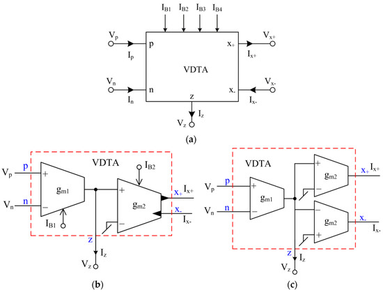
Figure 28.
Symbolic implementation and OTA-based implementations of the VDTA; (a) the symbolic representation; (b,c) two different VDTA implementations using OTAs.
In [35], Kumar, Pandey and Paul presented a number of VDTA-based inverse filters using two to four VDTAs along with two grounded capacitors without requiring any resistors, as preferred for IC implementation. A unified inverse filter structure from [35] is shown in Figure 29.
Figure 29.
Unified inverse filter topology employing VDTAs proposed by Kumar, Pandey and Paul [35].
The workability of all the realized inverse filters has been validated using CMOS VDTA with 0.18 µm CMOS technology parameters from TSMC over a frequency range of 100 kHz–100 MHz.
In another publication [36], the same authors presented another multifunction inverse filter similar to their earlier publication, which is shown in Figure 30 and contains three switches. By changing their positions, different filter functions can be achieved.
Figure 30.
VDTA-based universal multifunction inverse filter reported by Kumar, Pandey and Paul [36].
The workability of this configuration in its various modes has been demonstrated by SPICE simulation results and hardware results with VDTA realized by three LM13700-type IC OTAs, as per the schematic of Figure 28c. It is worth mentioning that the works [35,36] are the only ones where a study of total harmonic distortion and output noise variations has been investigated.
Lastly, it may be mentioned that, of late, there has been some interest in realizing fractional order inverse filters (FOIF) as well. It is obvious that the procedure applicable to fractional order normal filter design can also be applied on any inverse filter structure also to convert that into FOIF. Based upon this idea, a number of authors have recently come up with FOIF designs [76,77,78,79,80,81,82] using a variety of active elements. However, discussion of these is outside the scope of the present article.
In Table 1, we present a concise summary of the various inverse filter configurations discussed so far as a quick reference guide for the designers.

Table 1.
A concise comparison of various IAFs reviewed in this article.
4. The Unresolved Issues
The following issues related to inverse analog filters have not been addressed adequately in the open literature to date, and are therefore still open for further research and investigations.
In spite of considerable work reported in the published literature on analog inverse filters using a variety of ABBs, consideration of applying these structures to actual real-life practical applications has been very rare.
If one looks at the IBPF characterized by:
This can be re-written in the form of the following input–output equation:
which, in time-domain can be expressed as:
It therefore turns out that the IBP is the same thing as a PID controller. So, this is one practical application of IBP which can be considered to be known. However, to the best knowledge of the authors, except for the use of IBP filter as a PID controller, no explicit applications of any other types of inverse filters have so far been reported in the literature by anybody!
In this respect, it is worthwhile to mention that the synthesis of inverse filters on analog computers and their applications in the restoration and correction of time functions was carried out by Burch, Green and Grote in [6] as early as in 1964, i.e., before the easy commercial availability of the integrated circuit op-amps and any other IC circuit building blocks. Hence, it appears that the idea presented in [6] could now be attempted with the ready commercial availability of a large variety of analog circuit building blocks as the off-the-shelf ICs. Hence, putting all the ideas of the inverse filters to real-life practical applications is an unresolved and challenging problem which is still open to investigation.
It is worth mentioning that, with the exception of [35] and [36], the evaluation of the noise performance and dynamic range (DR) of IAFs have not been discussed in any of the earlier publications [1,7,8,9,10,11,12,13,14,15,16,17,18,19,20,21,22,23,24,25,26,27,28,29,30,31,32,33,34,35,36,37,38,39,40,41,42,43] on IAF so far, hence such data is not available for ant IAFs proposed in the quoted references. These aspects of most of the inverse filters proposed so far need further work.
Also, since the inverse filters feature (theoretically) infinite gain for some frequencies — for example, an inverse low-pass filter features infinite gain for high frequencies, and an inverse high-pass filter for low frequencies — this is a serious disadvantage, as very weak out-of-band signals may be amplified infinitely. Thus, the filter’s own noise as well as the supply rail interference may cause ‘clipping’. These aspects, too, need further investigation and resolution.
5. Concluding Remarks
This paper has presented a comprehensive survey of a variety of inverse active filters reported in the literature so far. The salient features of a number of prominent circuits using a variety of active building blocks, ranging from the classical voltage mode op-amp, the OTA, to the popular current mode building blocks such as current conveyors and their variants, the CFOA and a number of building blocks of more recent origin such as CDTA, OTRA, CDBA, CDTA and VDTA have been detailed and their merits and limitations have been spelled out. A number of unresolved problems/issues related to inverse analog filters were highlighted. We have attempted to demonstrate the need for finding a correlation between the coefficients of the various inverse transfer functions and the shape of the corresponding frequency responses. However, it is felt that additional research is needed to explore this issue further. The stability issues related to the first-order inverse all-pass filter and second-order IHP, IBR and IAP were pointed out. It was emphasized that further research is required to put most of the inverse filter types to practical use in real-life applications. In conclusion, the authors believe that a lot of research is still needed in order to bring the work done on inverse analog active filters [1,2,3,4,5,6,7,8,9,10,11,12,13,14,15,16,17,18,19,20,21,22,23,24,25,26,27,28,29,30,31,32,33,34,35,36,37,38,39,40,41,42,43] to a more practical footing.
Author Contributions
Conceptualization of this manuscript was by R.S.; the methodology by R.S., D.R.B. and A.R.; software verifications in SPICE by A.R.; validation by R.S., D.R.B. and A.R.; formal checking of the analysis by D.R.B. and A.R.; investigation by R.S.; resources by R.S., D.R.B. and A.R.; data curation by A.R.; writing—original draft preparation by R.S.; writing—review and editing by R.S., D.R.B. and A.R.; visualization by R.S.; supervision by R.S. and D.R.B.; project administration by R.S., D.R.B. and A.R. All authors have read and agreed to the published version of the manuscript.
Funding
This research received no external funding.
Acknowledgments
The first author (R.S.) wishes to thank Costas Psychalinos for extending the invitation to contribute a feature article for the special issue of this journal which was inspirational for the origin of this paper. The first author (R.S.) acknowledges the facilities provided by the ASP Research Lab. of the Department of ECE of NSUT and wishes to thank Tarun Rawat, S. P. Singh and Vice-Chancellor of NSUT J. P. Saini for the same. The other authors, namely, D.R.B. and A.R. acknowledge the facilities provided by ASP Lab. of the EE Department of Delhi Technological University (DTU) and wish to thank Pragati Kumar, Madhusudan Singh and Uma Nangia of the EE Department of DTU for their support. All the authors also wish to thank J. P. Saini, the Vice Chancellor of NSUT and DTU both, for his unflinching support. Thanks are due to all the anonymous reviewers for their constructive comments/suggestions which have been very useful in improving the presentation of this article. The authors particularly thank Reviewer # 4 for one of his very important comments, which we have taken the liberty of including nearly as-is, as the last paragraph of Section 4 of the revised version.
Conflicts of Interest
The authors declare that there is no conflict of interest.
References
- Leuciuc, A. Using nullors for realization of inverse transfer functions and characteristics. Electron. Lett. 1997, 33, 949–951. [Google Scholar] [CrossRef]
- Tugnait, J. Identification and deconvolution of multichannel linear non-Gaussian processes using higher order statistics and inverse filter criteria. IEEE Trans. Signal Process. 1997, 45, 658–672. [Google Scholar] [CrossRef]
- Kirkeby, O.; Nelson, P.A. Digital filter design for inversion problems in sound reproduction. J. Audio Eng. Soc. 1999, 47, 583–595. [Google Scholar]
- Watanabe, A. Formant estimation method using inverse-filter control. IEEE Trans. Speech Audio Process. 2001, 9, 317–326. [Google Scholar] [CrossRef]
- Zhang, Z.; Wang, D.; Wang, W.; Du, H.; Zu, J. A Group of Inverse Filters Based on Stabilized Solutions of Fredholm Integral Equations of the First Kind. In Proceedings of the 2008 IEEE Instrumentation and Measurement Technology Conference, Victoria, BC, Canada, 12–15 May 2008; pp. 668–671. [Google Scholar]
- Burch, J.; Green, A.; Grote, H. Restoration and Correction of Time Functions by the Synthesis of Inverse Filters on Analog Computers. IEEE Trans. Geosci. Electron. 1964, 2, 19–24. [Google Scholar] [CrossRef]
- Chipipop, B.; Surakampontorn, W. Realization of current-mode FTFN-based inverse filter. Electron. Lett. 1999, 35, 690–692. [Google Scholar] [CrossRef]
- Wang, H.-Y.; Lee, C.-T. Using nullors for realisation of current-mode FTFN-based inverse filters. Electron. Lett. 1999, 35, 1889–1890. [Google Scholar] [CrossRef]
- Abuelma’Atti, M.T. Identification of Cascadable Current-Mode Filters and Inverse-Filters Using Single FTFN. Frequenz 2000, 54, 284–289. [Google Scholar]
- Shah, N.A.; Malik, M.A. FTFN based dual inputs current-mode all pass inverse filters. Indian J. Radio Space Phys. 2005, 34, 206–209. [Google Scholar]
- Gupta, S.S.; Bhaskar, D.R.; Senani, R.; Singh, A.K. Inverse active filters employing CFOAs. Electr. Eng. 2009, 91, 23–26. [Google Scholar]
- Gupta, S.S.; Bhaskar, D.R.; Senani, R. New analogue inverse filters realized with current feedback op-amp. Int. J. Electron. 2011, 9, 1103–1113. [Google Scholar] [CrossRef]
- Wang, H.-Y.; Chang, S.-H.; Yang, T.-Y.; Tsai, P.-Y. A Novel Multifunction CFOA-Based Inverse Filter. Circuits Syst. 2011, 2, 14–17. [Google Scholar] [CrossRef]
- Garg, K.; Bhagat, R.; Jaint, B. A novel multifunction modified CFOA based inverse filter. In Proceedings of the 2012 IEEE 5th India International Conference on Power Electronics (IICPE), Delhi, India, 6–8 December 2012; pp. 1–5. [Google Scholar]
- Patil, V.N.; Sharma, R.K. Novel inverse active filters employing CFOA. Int. J. Sci. Res. Dev. 2015, 3, 359–360. [Google Scholar]
- Tsukutani, T.; Sumi, Y.; Yabuki, N. Electronically tunable inverse active filters employing OTAs and grounded capacitors. Int. J. Electron. Lett. 2014, 4, 166–176. [Google Scholar] [CrossRef]
- Raj, A.; Bhagat, R.; Kumar, P.; Bhaskar, D.R. Grounded-Capacitor Analog Inverse Active Filters using CMOS OTAs. In Proceedings of the 2021 8th International Conference on Signal Processing and Integrated Networks (SPIN), Noida, India, 26–27 August 2021; pp. 778–783. [Google Scholar]
- Tsukutani, T.; Kunugasa, Y.; Yabuki, N. CCII-Based Inverse Active Filters with Grounded Passive Components. J. Electr. Eng. 2018, 6, 212–215. [Google Scholar] [CrossRef][Green Version]
- Shah, N.A.; Rather, M.F. Realization of voltage-mode CCII-based all pass filter and its inversion version. Indian J. Pure Appl. Phys. 2006, 44, 269–271. [Google Scholar]
- Herencsar, N.; Lahiri, A.; Koton, J.; Vrba, K. Realizations of second-order inverse active filters using minimum passive components and DDCCs. In Proceedings of the 33rd International Conference on Telecommunications and Signal Processing-TSP, Vienna, Austria, 17–20 August 2010; pp. 38–41. [Google Scholar]
- Al-Absi, M.A. Realization of inverse filters using second generation voltage conveyor (VCII). Analog Integr. Circuits Signal Process. 2021, 109, 29–32. [Google Scholar] [CrossRef]
- Al-Shahrani, S.M.; Al-Absi, M.A. Efficient Inverse Filters based on Second-Generation Voltage Conveyor (VCII). Arab. J. Sci. Eng. 2021, 1–6. [Google Scholar] [CrossRef]
- Singh, A.K.; Gupta, A.; Senani, R. OTRA-Based Multi-Function Inverse Filter Configuration. Adv. Electr. Electron. Eng. 2018, 15, 846–856. [Google Scholar] [CrossRef]
- Pradhan, A.; Sharma, R.K. Generation of OTRA-Based Inverse All Pass and Inverse Band Reject Filters. Proc. Natl. Acad. Sci. India Sect. A Phys. Sci. 2019, 90, 481–491. [Google Scholar] [CrossRef]
- Banerjee, S.; Borah, S.S.; Ghosh, M.; Mondal, P. Three Novel Configurations of Second Order Inverse Band Reject Filter Using a Single Operational Transresistance Amplifier. In Proceedings of the TENCON 2019—2019 IEEE Region 10 Conference (TENCON), Kochi, India, 17–20 October 2019; pp. 2173–2178. [Google Scholar]
- Prasad, D.; Tayal, D.; Yadav, A.; Singla, L.; Haseeb, Z. CNTFET-based OTRA and its Application as Inverse Low Pass Filter. Int. J. Electron. Telecommun. 2019, 65, 665–670. [Google Scholar]
- Pandey, R.; Pandey, N.; Negi, T.; Garg, V. CDBA Based Universal Inverse Filter. ISRN Electron. 2013, 2013, 1–6. [Google Scholar] [CrossRef]
- Nasir, A.R.; Ahmad, S.N. A new current-mode multifunction inverse filter using CDBAs. Int. J. Comput. Sci. Inf. Secur. 2013, 11, 50–53. [Google Scholar]
- Bhagat, R.; Bhaskar, D.R.; Kumar, P. Inverse Band Reject and All Pass Filter Structure Employing CMOS CDBAs. Int. J. Eng. Res. Technol. 2019, 8, 39–44. [Google Scholar]
- Bhagat, R.; Bhaskar, D.R.; Kumar, P. Multifunction Filter/Inverse Filter Configuration Employing CMOS CDBAs. Int. J. Recent Technol. Eng. 2019, 8, 8844–8853. [Google Scholar]
- Borah, S.S.; Singh, A.; Ghosh, M. CMOS CDBA Based 6th Order Inverse Filter Realization for Low-Power Applications. In Proceedings of the 2020 IEEE Region 10 Conference (TENCON), Osaka, Japan, 16–19 November 2020; pp. 11–15. [Google Scholar]
- Paul, T.K.; Roy, S.; Pal, R.R. Realization of Inverse Active Filters Using Single Current Differencing Buffered Amplifier. J. Sci. Res. 2021, 13, 85–99. [Google Scholar] [CrossRef]
- Shah, N.A.; Quadri, M.; Iqbal, S.Z. High output impedance current-mode all pass inverse filter using CDTA. Indian J. Pure Appl. Phys. 2008, 46, 893–896. [Google Scholar]
- Sharma, A.; Kumar, A.; Whig, P. On performance of CDTA-based novel analog inverse low pass filter using 0.35 µm CMOS parameter. Int. J. Sci. Technol. Manag. 2015, 4, 594–601. [Google Scholar]
- Kumar, P.; Pandey, N.; Paul, S.K. Realization of Resistor less and Electronically Tunable Inverse Filters Using VDTA. J. Circ Syst. Comput. 2018, 28, 1950143. [Google Scholar] [CrossRef]
- Kumar, P.; Pandey, N.; Paul, S.K. Electronically Tunable VDTA-Based Multi-function Inverse Filter. Iran. J. Sci. Technol. Trans. Electr. Eng. 2021, 45, 247–257. [Google Scholar] [CrossRef]
- Kamat, D.V. New Operational Amplifier based Inverse Filters. In Proceedings of the 2019 3rd International conference on Electronics, Communication and Aerospace Technology (ICECA), Coimbatore, India, 12–14 June 2019; pp. 1177–1181. [Google Scholar]
- Freeborn, T.J.; Elwakil, A.S.; Maundy, B. Approximated fractional-order inverse Chebyshev low pass filters. Circuits Syst. Signal Process. 2016, 35, 1973–1982. [Google Scholar] [CrossRef]
- Bhaskar, D.R.; Kumar, M.; Kumar, P. Fractional order inverse filters using operational amplifier. Analog Integr. Circuits Signal Process. 2018, 97, 149–158. [Google Scholar] [CrossRef]
- Bhaskar, D.R.; Kumar, M.; Kumar, P. Minimal Realization of Fractional-Order Inverse Filters. IETE J. Res. 2020, 1–14. [Google Scholar] [CrossRef]
- Hamed, E.M.; Said, L.A.; Madian, A.H.; Radwan, A. On the Approximations of CFOA-Based Fractional-Order Inverse Filters. Circuits Syst. Signal Process. 2019, 39, 2–29. [Google Scholar] [CrossRef]
- Kumar, M.; Bhaskar, D.R.; Kumar, P. CFOA-Based New Structure of Fractional Order Inverse Filters. Int. J. Recent Technol. Eng. 2020, 8, 2277–3878. [Google Scholar]
- Srivastava, J.; Bhagat, R.; Kumar, P. Analog Inverse Filters Using OTAs. In Proceedings of the 2020 6th International Conference on Control, Automation and Robotics (ICCAR), Singapore, 20–23 April 2020; pp. 627–631. [Google Scholar]
- Senani, R. Generation of new two-amplifier synthetic floating inductors. Electron. Lett. 1987, 23, 1202–1203. [Google Scholar] [CrossRef]
- Senani, R. A novel application of four-terminal floating nullors. Proc. IEEE 1987, 75, 1544–1546. [Google Scholar] [CrossRef]
- Wheatley, C.F.; Wittlinger, H.A. OTA obsolete op-amp. Proc. Nat. Electron. Conf. 1969, 4159, 152–157. [Google Scholar]
- Smith, K.; Sedra, A. The current conveyor—A new circuit building block. Proc. IEEE 1968, 56, 1368–1369. [Google Scholar] [CrossRef]
- Sedra, A.; Smith, K. A second-generation current conveyor and its applications. IEEE Trans. Circuit Theory 1970, 17, 132–134. [Google Scholar] [CrossRef]
- AD844: 60 MHz, 2000 V/µs, Monolithic Op Amp with Quad Low Noise Data Sheet (Rev. G). May 2017. Available online: www.linear.com (accessed on 29 April 2019).
- Chen, J.-J.; Tsao, H.-W.; Chen, C.-C. Operational transresistance amplifier using CMOS technology. Electron. Lett. 1992, 28, 2087–2088. [Google Scholar] [CrossRef]
- Acar, C.; Ozoguz, S. A new versatile building block: Current differencing buffered amplifier suitable for analog signal-processing filters. Microelectron. J. 1999, 30, 157–160. [Google Scholar] [CrossRef]
- Biolek, D. CDTA-building block for current-mode analog signal processing. In Proceedings of the 16th European Conference on Circuits Theory and Design, ECCTD’03, Krakow, Poland, 1–4 September 2003; Volume III, pp. 397–400. [Google Scholar]
- Biolek, D.; Senani, R.; Biolková, V.; Kolka, Z. Active elements for analog signal processing: Classification, review, and new proposals. Radioengineering 2008, 17, 15–32. [Google Scholar]
- Carlin, H.J.; Youla, D. Network Synthesis with Negative Resistors. Proc. IRE 1961, 49, 907–920. [Google Scholar] [CrossRef]
- Mitra, S.K. A network transformation for active RC networks. Proc. IEEE 1967, 55, 2021–2022. [Google Scholar] [CrossRef]
- Rathore, T.S. Inverse active networks. Electron. Lett. 1977, 13, 303–304. [Google Scholar] [CrossRef]
- Rathore, T.S.; Singhi, B.M. Network transformations. IEEE Trans. Circuits Syst. 1980, 27, 57–59. [Google Scholar] [CrossRef]
- Higashimura, M. Realisation of current-mode transfer function using four-terminal floating nullor. Electron. Lett. 1991, 27, 170–171. [Google Scholar] [CrossRef]
- Normand, G. Floating-impedance realisation using a dual operational-mirrored amplifier. Electron. Lett. 1986, 22, 521–522. [Google Scholar] [CrossRef]
- Anandamohan, P.V. New current-mode biquad on Friend-Deliyannis active RC biquad. IEEE Trans. Circ. Syst. II Analog Digit. Signal Process. 1995, 42, 225–228. [Google Scholar]
- Toumazou, C.; Lidgey, F.J. Current-Feedback Op-Amps-A blessing in disguise. IEEE Circ. Dev. Mag. 1997, 10, 34–37. [Google Scholar]
- Lidgey, F.J.; Hayatleh, K. Current-feedback operational amplifiers and applications. Electron. Commun. Eng. J. 1997, 9, 176–182. [Google Scholar] [CrossRef]
- Soliman, A.M. Applications of the current feedback operational amplifiers. Analog Integr. Circuits Signal Process. 1996, 11, 265–302. [Google Scholar] [CrossRef]
- Senani, R. Realisation of a Class of Analog Signal Processing/Signal Generation Circuits: Novel Configurations Using Current Feedback Op-Amps. Frequenz 1998, 52, 196–206. [Google Scholar] [CrossRef]
- Senani, R.; Bhaskar, D.R.; Singh, A.K. Current Feedback Operational Amplifiers and Their Applications; Springer Science and Business Media LLC: Berlin/Heidelberg, Germany, 2013. [Google Scholar]
- Bhushan, M.; Newcomb, R.W. Grounding of capacitors in integrated circuits. Electron. Lett. 1967, 3, 148–149. [Google Scholar] [CrossRef]
- Newcomb, R.W. Active Integrated Circuit Synthesis; Prentice-Hall: Hoboken, NJ, USA, 1967. [Google Scholar]
- Gupta, S.S.; Senani, R. Realization of Current-mode SRCOs using All Grounded Passive Elements. Freq. J. Telecommun. 2003, 57, 26–37. [Google Scholar]
- Sharma, R.K.; Senani, R. Multifunction CM/VM Biquads Realized with a Single CFOA and Grounded Capacitors. AEU Int. J. Electron. Commun. 2003, 57, 301–308. [Google Scholar] [CrossRef]
- Yuce, E.; Minaei, S. A Modified CFOA and Its Applications to Simulated Inductors, Capacitance Multipliers, and Analog Filters. IEEE Trans. Circuits Syst. I Regul. Pap. 2008, 55, 266–275. [Google Scholar] [CrossRef]
- Swamy, M.N.S. Modified CFOA, its transpose, and applications. Int. J. Circuit Theory Appl. 2015, 44, 514–526. [Google Scholar] [CrossRef]
- Smith, K.; Sedra, A. Realization of the Chua family of new nonlinear network elements using the current conveyor. IEEE Trans. Circuit Theory 1970, 17, 137–139. [Google Scholar] [CrossRef]
- Chiu, W.; Liu, S.I.; Tsao, H.W.; Chen, J.J. CMOS differential difference current conveyors and their applications. IEE Proc. Circuits Devices Syst. 1996, 143, 91–96. [Google Scholar] [CrossRef]
- Čajka, J.; Vrba, K. The voltage conveyor may have in fact found its way into circuit theory. AEU—Int. J. Electron. Commun. 2004, 58, 244–248. [Google Scholar] [CrossRef]
- Safari, L.; Yuce, E.; Minaei, S.; Ferri, G.; Stornelli, V. A second-generation voltage conveyor (VCII)-based simulated grounded inductor. Int. J. Circuit Theory Appl. 2020, 48, 1180–1193. [Google Scholar] [CrossRef]
- Radwan, A.; Soliman, A.M.; Elwakil, A.S.; Sedeek, A. On the stability of linear systems with fractional-order elements. Chaos Solitons Fractals 2009, 40, 2317–2328. [Google Scholar] [CrossRef]
- Elwakil, A.S. Fractional-Order Circuits and Systems: An Emerging Interdisciplinary Research Area. IEEE Circuits Syst. Mag. 2010, 10, 40–50. [Google Scholar] [CrossRef]
- Tsirimokou, G.; Psychalinos, C. Ultra-low voltage fractional-order circuits using current mirrors. Int. J. Circuit Theory Appl. 2016, 44, 109–126. [Google Scholar] [CrossRef]
- Adhikary, A.; Sen, S.; Biswas, K. Practical Realization of Tunable Fractional Order Parallel Resonator and Fractional Order Filters. IEEE Trans. Circuits Syst. I Regul. Pap. 2016, 63, 1142–1151. [Google Scholar] [CrossRef]
- Kartci, A.; Herencsar, N.; Koton, J.; Brancik, L.; Vrba, K.; Tsirimokou, G.; Psychalinos, C. Fractional-order oscillator design using unity-gain voltage buffers and OTAs. In Proceedings of the 2017 IEEE 60th International Midwest Symposium on Circuits and Systems (MWSCAS), Boston, MA, USA, 6–9 August 2017; pp. 555–558. [Google Scholar]
- Tsirimokou, G.; Psychalinos, C.; Elwakil, A.S. Design of CMOS Analog Integrated Fractional-Order Circuits: Applications in Medicine and Biology; Springer: Berlin/Heidelberg, Germany, 2017. [Google Scholar]
- Varshney, G.; Pandey, N.; Pandey, R. Electronically Tunable Multifunction Transadmittance-Mode Fractional-Order Filter. Arab. J. Sci. Eng. 2021, 46, 1067–1078. [Google Scholar] [CrossRef]
Publisher’s Note: MDPI stays neutral with regard to jurisdictional claims in published maps and institutional affiliations. |
© 2022 by the authors. Licensee MDPI, Basel, Switzerland. This article is an open access article distributed under the terms and conditions of the Creative Commons Attribution (CC BY) license (https://creativecommons.org/licenses/by/4.0/).