
CMOS Perceptron for Vesicle Fusion Classification


Abstract
:1. Introduction
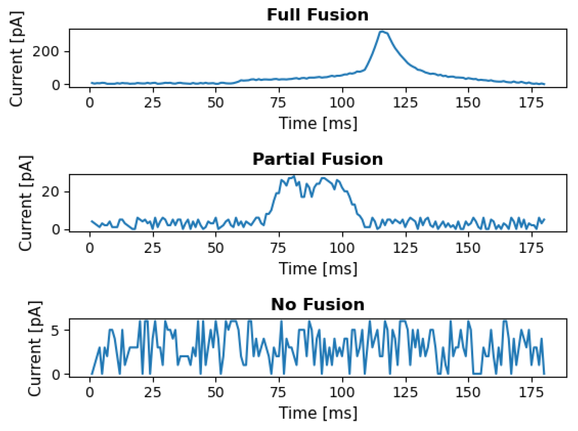
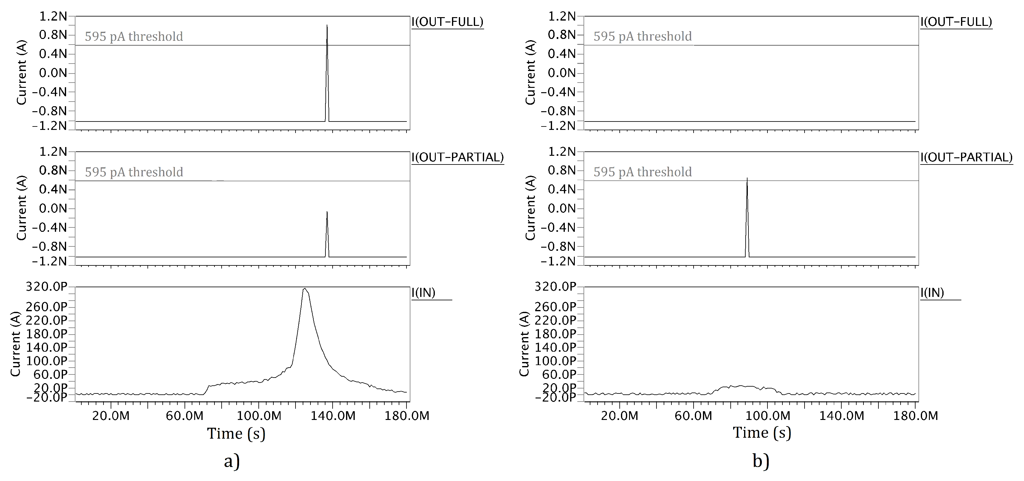
2. Vesicle Fusion
3. Weak Inversion Mode
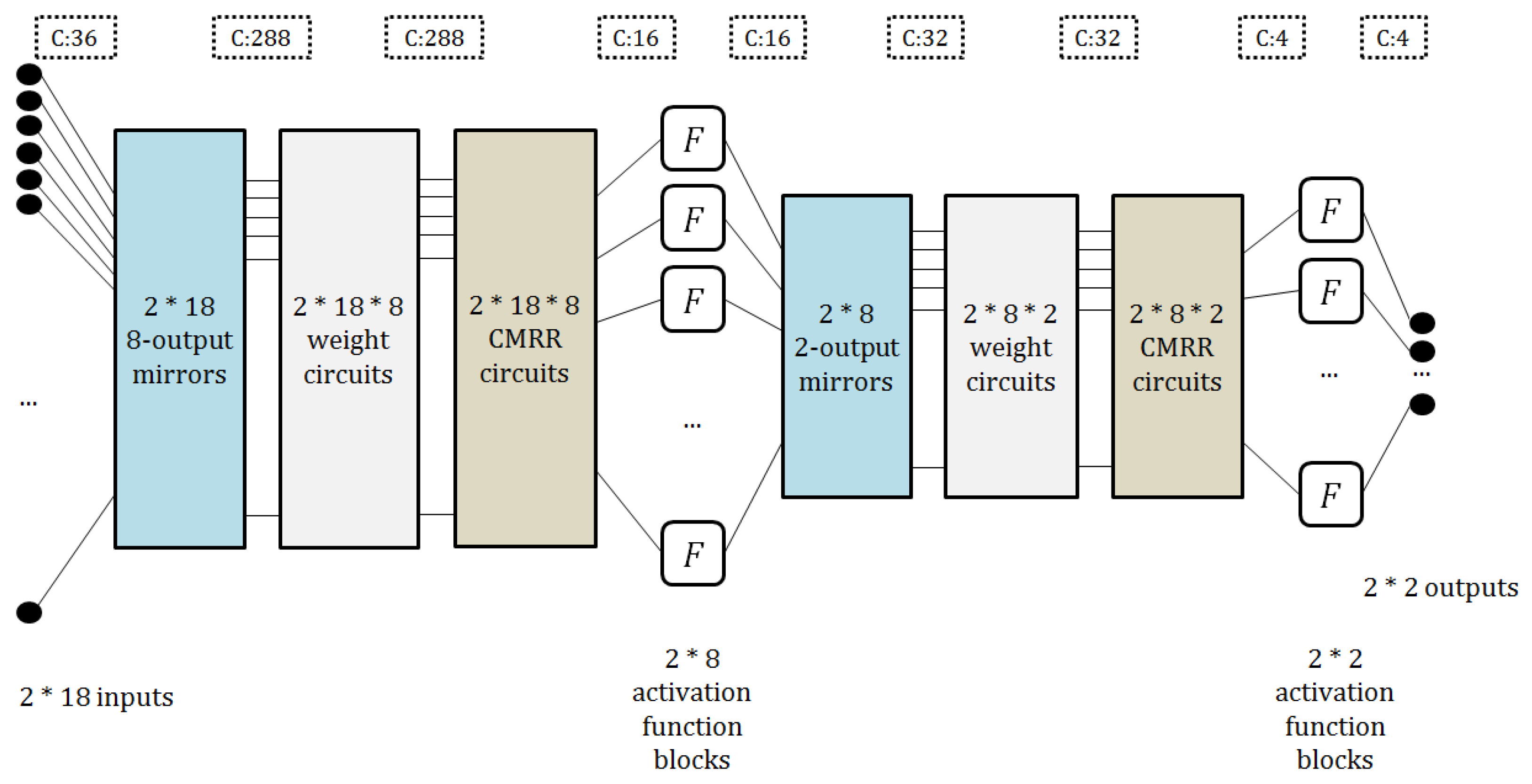
4. Network Structure
4.1. Dataset Description
4.2. Architecture
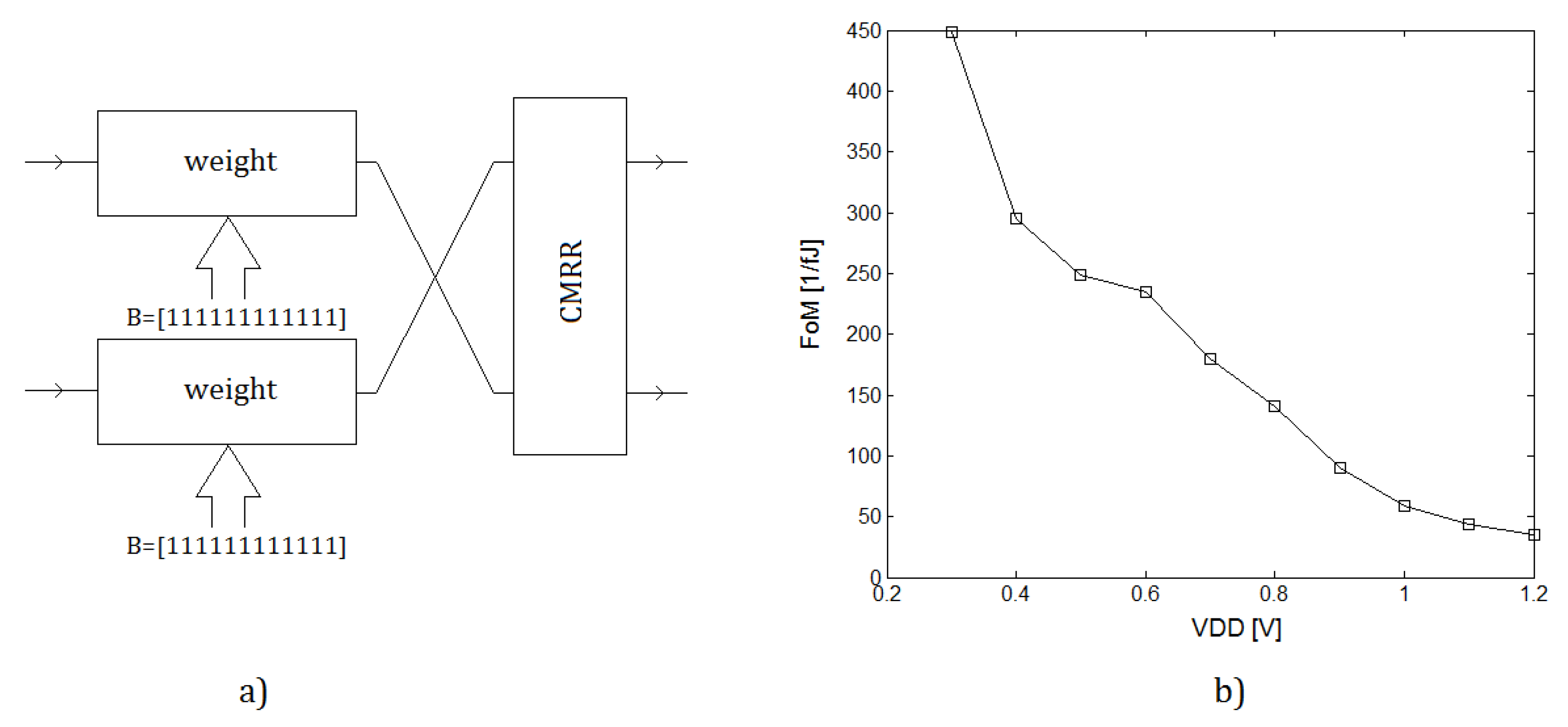
4.3. Learning
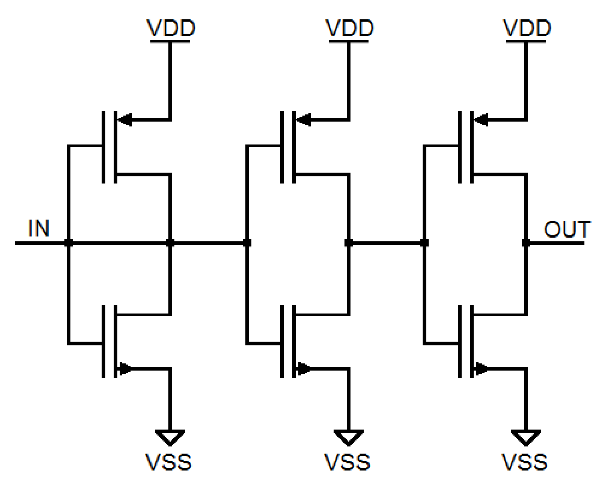
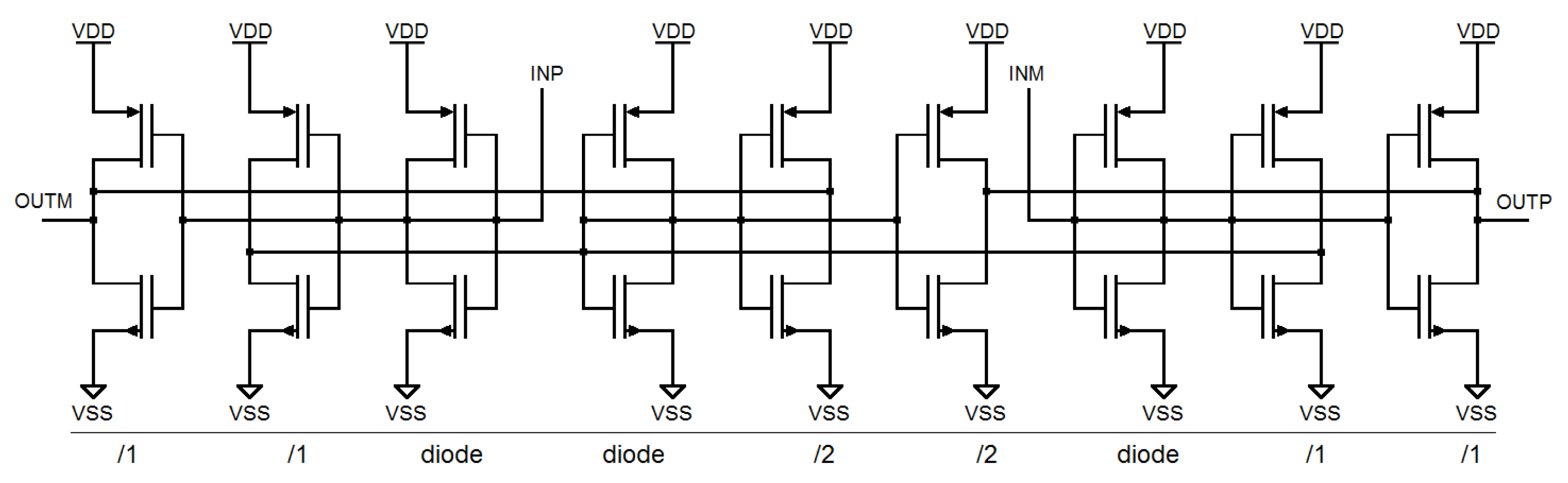
5. CMOS Classifier Parameters
6. Conclusions
Author Contributions
Funding
Data Availability Statement
Conflicts of Interest
Abbreviations
| Edge-AI | Edge Artificial Intelligence |
| AFE | Analog Front-End |
| AUC | Area Under the Curve |
| CMOS | Complementary Metal-Oxide-Semiconductor |
| CMRR | Common Mode Rejection Ratio |
| CNT | Carbon Nanotube |
| DAC | Digital-to-Analog Converter |
| EDA | Electronic Design Automation |
| FoM | Figure of Merit |
| HCNN | Hierarchical Convolutional Neural Network |
| IP | Intellectual Property |
| NC | Number of Channels |
| ROC | Receiver Operating Characteristic |
| TinyML | Tiny Machine Learning |
| TIRF | Total Internal Reflection Fluorescence |
| TSMC | Taiwan Semiconductor Manufacturing Company |
| VLSI | Very Large-Scale Integration |
| WTA | Winner Takes All |
References
- van der Meulen, R.; Gartner Research. What Edge Computing Means for Infrastructure and Operations Leaders. 2018. Available online: https://www.gartner.com/smarterwithgartner/what-edge-computing-means-for-infrastructure-and-operations-leaders (accessed on 30 January 2022).
- Weisong, S.; Hui, S.; Jie, C.; Quan, Z.; Wei, L. Edge Computing—An Emerging Computing Model for the Internet of Everything Era. J. Comput. Res. Dev. 2017, 54, 907–924. [Google Scholar]
- Xu, J.; Palanisamy, B.; Ludwig, H.; Wang, Q. Zenith: Utility-Aware Resource Allocation for Edge Computing. In Proceedings of the 2017 IEEE International Conference on Edge Computing (EDGE), Honolulu, HI, USA, 25–30 June 2017; pp. 47–54. [Google Scholar]
- Cui, G.; He, Q.; Li, B.; Xia, X.; Chen, F.; Jin, H.; Xiang, Y.; Yang, Y. Efficient Verification of Edge Data Integrity in Edge Computing Environment. IEEE Trans. Serv. Comput. 2021. [Google Scholar] [CrossRef]
- Sun, L.; Jiang, X.; Ren, H.; Guo, Y. Edge-Cloud Computing and Artificial Intelligence in Internet of Medical Things: Architecture, Technology and Application. IEEE Access 2020, 8, 101079–101092. [Google Scholar] [CrossRef]
- Zida, S.I.; Lin, Y.-D.; Lee, C.L.; Tsai, Y.L. Evaluation of an Intelligent Edge Computing System for the Hospital Intensive Care Unit. In Proceedings of the IEEE 3rd Eurasia Conference on Biomedical Engineering, Healthcare and Sustainability (ECBIOS), Tainan, Taiwan, 28–30 May 2021. [Google Scholar]
- Javaid, S.; Zeadally, S.; Fahim, H.; He, B. Medical sensors and their integration in Wireless Body Area Networks for Pervasive Healthcare Delivery: A Review. IEEE Sensors J. 2022, 22, 3860–3877. [Google Scholar] [CrossRef]
- Chandrasekhara Reddy, T.; Sirisha, G.; Reddy, A.M. Smart Healthcare Analysis and Therapy for Voice Disorder using Cloud and Edge Computing. In Proceedings of the 4th International Conference on Applied and Theoretical Computing and Communication Technology (iCATccT), Mangalore, India, 6–8 September 2018. [Google Scholar]
- Liu, X.; Zhou, P.; Qiu, T.; Wu, D.O. Blockchain-Enabled Contextual Online Learning Under Local Differential Privacy for Coronary Heart Disease Diagnosis in Mobile Edge Computing. IEEE J. Biomed. Health Inform. 2020, 24, 2177–2188. [Google Scholar] [CrossRef]
- Barua, A.; Dong, C.; Al-Turjman, F.; Yang, X. Edge Computing-Based Localization Technique to Detecting Behavior of Dementia. IEEE Access 2020, 8, 82108–82119. [Google Scholar] [CrossRef]
- Namee, K.; Panong, N.; Polpinij, J. Integration of IoT, Edge Computing and Cloud Computing for Monitoring and Controlling Automated External Defibrillator Cabinets in Emergency Medical Service. In Proceedings of the 5th International Conference on Information Management (ICIM), Cambridge, UK, 24–27 March 2019. [Google Scholar]
- Palm, W.; Thompson, C.B. Nutrient acquisition strategies of mammalian cells. Nature 2017, 546, 234–242. [Google Scholar] [CrossRef]
- Jou, A.Y.-S.; Pajouhi, H.; Azadegan, R.; Mohammadi, S. A CMOS integrated rectenna for implantable applications. In Proceedings of the IEEE MTT-S International Microwave Symposium (IMS), San Francisco, CA, USA, 22–27 May 2016. [Google Scholar]
- Abden, S.; Azab, E. Multilayer Perceptron Analog Hardware Implementation Using Low Power Operational Transconductance Amplifier. In Proceedings of the 32nd International Conference on Microelectronics (ICM), Aqaba, Jordan, 14–17 December 2020. [Google Scholar]
- Ishiguchi, Y.; Isogai, D.; Osawa, T.; Nakatake, S. A Perceptron Circuit with DAC-Based Multiplier for Sensor Analog Front-Ends. In Proceedings of the New Generation of CAS (NGCAS), Genova, Italy, 6–9 September 2017. [Google Scholar]
- Kumar, P.; Zhu, K.; Gao, X.; Wang, S.D.; Lanza, M.; Thakur, C.S. Hybrid architecture based on two-dimensional memristor crossbar array and CMOS integrated circuit for edge computing. 2D Mater. Appl. 2022, 6, 1–10. [Google Scholar] [CrossRef]
- Wong, H.P.; Dahari, Z. Human body parts heat energy harvesting using thermoelectric module. In Proceedings of the IEEE Conference on Energy Conversion (CENCON), Johor Bahru, Malaysia, 19–20 October 2015. [Google Scholar]
- Oh, N.; Park, J.H. Endocytosis and exocytosis of nanoparticles in mammalian cells. Int. J. Nanomed. 2013, 9 (Suppl. 1), 51–63. [Google Scholar]
- Ivan, A.I. (Ed.) Exocytosis and Endocytosis, 2nd ed.; International Institute of Anticancer Research; Humana Press: Totowa, NJ, USA; Springer Science and Business Media: Berlin/Heidelberg, Germany, 2014; Volume 3, p. 435. [Google Scholar]
- Lucien, F.; Leong, H.S. The role of extracellular vesicles in cancer microenvironment and metastasis: Myths and challenges. Biochem. Soc. Trans. 2019, 47, 273–280. [Google Scholar] [CrossRef] [PubMed]
- Zoltowska, K.M.; Maesako, M.; Lushnikova, I.; Takeda, S.; Keller, L.J.; Skibo, G.; Hyman, B.T.; Berezovska, O. Dynamic presenilin 1 and synaptotagmin 1 interaction modulates exocytosis and amyloid β production. Mol. Neurodegener. 2017, 12, 15. [Google Scholar] [CrossRef] [PubMed] [Green Version]
- Michels, A.; Albánez, S.; Mewburn, J.; Nesbitt, K.; Gould, T.J.; Liaw, P.C.; James, P.D.; Swystun, L.L.; Lillicrap, D. Histones link inflammation and thrombosis through the induction of Weibel–Palade body exocytosis. J. Thromb. Haemost. 2016, 14, 2274–2286. [Google Scholar] [CrossRef] [PubMed]
- Liang, K.; Wei, L.; Chen, L. Exocytosis, Endocytosis, and Their Coupling in Excitable Cells. Front. Mol. Neurosci. 2017, 10, 109. [Google Scholar] [CrossRef] [Green Version]
- Ahmed, K.A.; Xiang, J. Mechanisms of cellular communication through intercellular protein transfer. Cell. Mol. Med. 2011, 15, 1458–1473. [Google Scholar] [CrossRef] [PubMed]
- Ren, L.; Mellander, L.J.; Keighron, J.; Cans, A.-S.; Kurczy, M.E.; Svir, I.; Oleinick, A.; Amatore, C.; Ewing, A.G. The evidence for open and closed exocytosisas the primary release mechanism. Q. Rev. Biophys. 2016, 49, e12. [Google Scholar] [CrossRef] [Green Version]
- Schneckenburger, H. Total internal reflection fluorescence microscopy: Technical innovations and novel applications. Curr. Opin. Cell Biol. 2005, 16, 13–18. [Google Scholar] [CrossRef]
- Li, H.; Yin, Z.; Xu, Y. A deep learning framework for automated vesicle fusion detection. In Proceedings of the IEEE International Symposium on Biomedical Imaging, Melbourne, Australia, 18–21 April 2017. [Google Scholar]
- Li, H.; Mao, Y.; Yin, Z.; Xu, Y. A hierarchical convolutional neural network for vesicle fusion event classification. Comput. Med. Imaging Graph. 2017, 60, 22–34. [Google Scholar] [CrossRef]
- Amine, A.; Mohammadi, H.; Amperometry, H. Encyclopedia of Analytical Science, 3rd ed.; Elsevier: New York, NY, USA, 2019; pp. 85–98. [Google Scholar]
- Szczęsny, S.; Pietrzak, P. Exocytotic vesicle fusion classification for early disease diagnosis using a mobile GPU microsystem. Neural Comput. Appl. 2022, 34, 4843–4854. [Google Scholar] [CrossRef]
- Fan, S.; Liang, W.; Dang, H.; Franklin, N.; Tombler, T.; Chapline, M.; Dai, H. Carbon nanotube arrays on silicon substrates and their possible application. Physica E 2000, 8, 179–183. [Google Scholar] [CrossRef]
- Li, J.; Meyyappan, M.; Cassell, A.M. Biochemical Sensors Using Carbon Nanotube Arrays. U.S. Patent 7,939,734, 10 May 2011. [Google Scholar]
- Biochemical Sensors Using Carbon Nanotube Arrays. Available online: https://technology.nasa.gov/patent/TOP2-104 (accessed on 17 January 2022).
- Fathail, H.; Cans, A.S. Amperometry methods for monitoring vesicular quantal size and regulation of exocytosis release. Pflug. Arch. 2018, 470, 125–134. [Google Scholar] [CrossRef] [PubMed] [Green Version]
- Chen, Y.C.; Lu, S.Y.; Tsai, J.H.; Liao, Y.T. A Power-Efficient, Bi-Directional Readout Interface Circuit for Cyclic-Voltammetry Electrochemical Sensors. In Proceedings of the 2019 International Symposium on VLSI Design, Automation and Test (VLSI-DAT), Hsinchu, Taiwan, 22–25 April 2019. [Google Scholar]
- Handkiewicz, A.; Szczęsny, S.; Kropidłowski, M. Over rail-to-rail fully differential voltage-to-current converters for nm scale CMOS technology. Analog. Integr. Circuits Signal Process. 2018, 94, 139–146. [Google Scholar] [CrossRef]
- Harrison, R. MOSFET Operation in Weak and Moderate Inversion; EE5720; University of Utah: Salt Lake City, UT, USA, 2014. [Google Scholar]
- Szczęsny, S.; Kropidłowksi, M.; Naumowicz, M. 0.50-V Ultra-Low-Power ΣΔ Modulator for Sub-nA Signal Sensing in Amperometry. IEEE Sensors J. 2020, 20, 5733–5740. [Google Scholar] [CrossRef]
- Cracan, A.; Bonteanu, G.; Bozomitu, R.G. A Weak-Inversion CMOS Analog Multiplier/Divider Circuit. In Proceedings of the IEEE 24th International Symposium for Design and Technology in Electronic Packaging (SIITME), Iasi, Romania, 25–28 October 2018. [Google Scholar]
- Aiyappa, B.N.; Madhusudan, M.; Yashaswini, B.; Yatish, R.; Nithin, M. Amplifier design in weak inversion and strong inversion—A case study. In Proceedings of the International Conference on Communication and Signal Processing (ICCSP), Chennai, India, 6–8 April 2017. [Google Scholar]
- Fan, H.; Lei, P.; Yang, J.; Feng, Q.; Wei, Q.; Su, H.; Wang, G. A high-efficient dynamic comparator with low-offset in weak inversion region. Analog. Integr. Circuits Signal Process. 2021, 110, 175–183. [Google Scholar] [CrossRef]
- Szczęsny, S. 0.3 V 2.5 nW per Channel Current-Mode CMOS Perceptron for Biomedical Signal Processing in Amperometry. IEEE Sens. J. 2017, 17, 5399–5409. [Google Scholar] [CrossRef]
- Szczęsny, S. High speed and low sensitive current-mode CMOS perceptron. Microelectron. Eng. 2016, 165, 41–51. [Google Scholar] [CrossRef]
- Szczęsny, S. HDL-Based Synthesis System with Debugger for Current-Mode FPAA. IEEE Trans. Comput. Aided Des. Integr. Circuits Syst. 2018, 37, 915–926. [Google Scholar] [CrossRef]
- Pan, H.C.; Hsieh, H.Y.; Tang, K.T. An analog multilayer perceptron neural network for a portable electronic nose. Sensors 2013, 13, 193–207. [Google Scholar] [CrossRef]
- Rasouli, M.; Yi, C.; Basu, A.; Thakor, N.V.; Kukreja, S. Spike-based tactile pattern recognition using an extreme learning machine. In Proceedings of the 2015 IEEE Biomedical Circuits and Systems Conference (BioCAS), Atlanta, GA, USA, 22–24 October 2015; pp. 1–4. [Google Scholar]
- Talaśka, T.; Kolasa, M.; Długosz, R.; Pedrycz, W. Analog programmable distance calculation circuit for winner takes all neural network realized in the CMOS technology. IEEE Trans. Neural Netw. Learn. Syst. 2016, 27, 661–673. [Google Scholar] [CrossRef]
- Shafique, M.; Theocharides, T.; Reddy, V.J.; Murmann, B. TinyML: Current Progress, Research Challenges, and Future Roadmap. In Proceedings of the 58th ACM/IEEE Design Automation Conference (DAC), San Francisco, CA, USA, 5–9 December 2021. [Google Scholar]
- Ooko, S.O.; Ogore, M.M.; Nsenga, J.; Zennaro, M. TinyML in Africa: Opportunities and Challenges. In Proceedings of the IEEE Globecom Workshops (GC Wkshps), Madrid, Spain, 7–11 December 2021. [Google Scholar]


Publisher’s Note: MDPI stays neutral with regard to jurisdictional claims in published maps and institutional affiliations. |
© 2022 by the authors. Licensee MDPI, Basel, Switzerland. This article is an open access article distributed under the terms and conditions of the Creative Commons Attribution (CC BY) license (https://creativecommons.org/licenses/by/4.0/).
Share and Cite
Naumowicz, M.; Pietrzak, P.; Szczęsny, S.; Huderek, D. CMOS Perceptron for Vesicle Fusion Classification. Electronics 2022, 11, 843. https://doi.org/10.3390/electronics11060843
Naumowicz M, Pietrzak P, Szczęsny S, Huderek D. CMOS Perceptron for Vesicle Fusion Classification. Electronics. 2022; 11(6):843. https://doi.org/10.3390/electronics11060843
Chicago/Turabian StyleNaumowicz, Mariusz, Paweł Pietrzak, Szymon Szczęsny, and Damian Huderek. 2022. "CMOS Perceptron for Vesicle Fusion Classification" Electronics 11, no. 6: 843. https://doi.org/10.3390/electronics11060843
APA StyleNaumowicz, M., Pietrzak, P., Szczęsny, S., & Huderek, D. (2022). CMOS Perceptron for Vesicle Fusion Classification. Electronics, 11(6), 843. https://doi.org/10.3390/electronics11060843