Abstract
In this paper, a new implementation of an electronically tunable resistor-less floating inductance simulator using a second-generation voltage conveyor (VCII) is presented. The proposed circuit is resistor-free (benefiting from the intrinsic resistors at the Y terminals of the employed VCIIs) and composed of three VCIIs and a single grounded capacitor. Using a control current (Icon), the value of impedance at the Y terminal of the VCII is varied, whereby the value of the simulated inductance is tuned. The proposed circuit is designed at a transistor level using 0.18 µm TSMC CMOS parameters and ±0.9 V supply voltage. PSpice simulations are carried out to confirm the effectiveness of the proposed circuit. For a range of Icon from 0 µA to 50 µA, the value of the simulated L can be varied from −576 µH to −324 µH and from +316 µH to +576 µH for negative and positive simulators, respectively, in the frequency range of 100 kHz–3 MHz. Favorably, the value of the series resistance remains below 76 Ω. Simulation results show an error value below 4.8% and power consumption variation is from 1.64 mW to 1.92 mW. Moreover, application of the proposed circuit as a standard band-pass RLC filter is also included.
1. Introduction
In the integrated circuit technology, the use of inductors, especially with large values, is impractical, mainly due to the large-occupied area. Accordingly, instead of bulky physical inductors, simulated inductors are used to overcome this problem. In this approach, active building blocks (ABBs) along with capacitors and resistors are used to synthesize the equivalent of inductors in a specified frequency range. More importantly, unlike physical inductors which suffer from a limited adjustment range of 15% [1], the value of simulated inductors can be easily adjusted. For those with electronic tuning capability, it is possible to adjust the value of simulated inductors electronically through a control current or voltage which is considered advantageous for providing full integration. Floating and grounded simulated inductors find wide applications in the design of filters and oscillators as well as in the cancellation of unavoidable parasitic capacitances [1,2,3,4]. The industry’s recent trend toward integration and miniaturization has made the inductance simulator design a popular research topic.
A survey of recent literature reveals that various approaches are used in the realization of floating inductors [5,6,7,8,9,10,11,12,13,14,15]. In [5], a digitally tunable floating inductor using two current differential amplifiers (CDAs), two resistors and an array of five floating capacitors, each one connected to a switch, is reported. The value of the achieved inductor is changed by controlling the bits applied to the switches. The main drawback of this approach is the large number of floating capacitors used in the implementation and the need for digital controlling. Another approach based on four second-generation current conveyors (CCIIs), one grounded capacitor, two grounded resistors and an array of ten floating resistors, each one connected to a switch, is reported in [6] for a digitally programmable floating inductance. The equivalent value of the resistor array is changed by controlling the bits applied to the switches; therefore, the value of the achieved simulated inductor is defined. Compared to the digitally programmable floating inductor of [5], the circuit of [6] does not employ floating capacitors. However, its operation depends on the matching between two resistors connected to the Y and X terminals of the first CCII. Moreover, to precisely define the value of the achieved inductor, the value of the resistors connected to switches must be trimmed carefully. The solution reported in [7] utilizes three current differencing transconductance amplifiers (CDTAs) and one grounded capacitor. Electronic tunability is achieved by changing the transconductance of the used ABBs through increasing the bias current, which results in high power consumption. In [8], only one differential voltage current conveyor transconductance amplifier (DVCCTA) is used as ABB. Electronic tuning is performed through increasing the bias current, which sacrifices power consumption and the quality of the achieved inductor. The latter occurs because, by increasing the bias current, the value of the parasitic resistors connected in parallel to the simulated inductor are reduced, which limits its overall performance. In [9], one dual output differential difference current conveyor (DO-DDCC), two resistors and one grounded capacitor are used to design a floating inductor simulator. Unfortunately, the achieved inductance lacks electronic tuning capability, and its operation relies on the matching between the used resistors. The topology reported in [10] utilizes one differential voltage current conveyor (DVCC), one current controlled current conveyor (CCCII), one grounded resistor and one floating capacitor. Using the electronic controlling capability of CCCII, the achieved inductor is electronically tunable. However, as the bias current is increased to change the value of the achieved inductor, power consumption is increased accordingly. In addition, the topology is not desirable from an integration point of view due to the used floating capacitor. In [11], an attempt is made to design a floating inductor simulator using active building blocks only, which utilizes one current controlled conveyor transconductance amplifier (CCCTA) and one operational amplifier (OA). Although it is claimed that the proposed topology is capacitor free, its operation relies on the compensation capacitor used in the internal structure of OA. In addition, the circuit suffers from high power consumption and limited frequency range due to the limited frequency performance of OA. In [12], two differential voltage-to-current converters, two resistors and one capacitor are used. In [13], another topology using two differential difference current conveyors, two resistors and one grounded capacitor is introduced. The circuit reported in [14] employs two modified current feedback operational amplifiers (MCFOAs), two resistors and one grounded capacitor. The main weakness of [12,13,14] is the lack of electronic tunability. In [15], a different topology based on CCII±, one dual output transconductance amplifier (DO-OTA), one resistor and one floating capacitor is used. It is electronically tunable, but it employs a floating capacitor. In addition, as the bias current of DO-OTA is increased to tune the value of the simulated capacitor, the value of the parasitic parallel resistors is reduced, which causes the quality of the simulated inductor to deteriorate.
Recently, a new active building block called a second-generation voltage conveyor (VCII) [16,17,18,19,20], which is the dual circuit of well-known CCII, has been employed in the design of grounded impedance simulators [21,22]. Comparison shows that the simulated grounded capacitors and inductors using VCII exhibit many advantages, namely, simpler realizations, reduced error, reduced parasitics, lower power consumption, etc., over simulated grounded impedances utilized by other ABBs. From the reported results in [21,22], the use of VCII in realizing impedance simulators looks quite promising. In this paper, we aim to employ VCII in realizing a floating inductor simulator. The proposed topology is resistor-less and uses three VCIIs and one grounded capacitor. Instead of passive resistors, the internal resistors at the Y terminals of the used ABBs are used. The proposed topology has the capability to simulate both positive and negative inductors. The value of the simulated inductor is easily adjusted by a control current which is used to change the value of the Y terminal impedance of the used VCIIs. To provide low voltage operation, the bias current is increased only in the input section of VCII and the bias current in the other sections remains constant. Therefore, by increasing the control current, the parallel parasitic resistors associated with the simulated inductor will not experience any reduction, thereby resulting in high performance. The circuit enjoys a simple resistor-free realization made of 52 transistors in total. The reduced error, low parasitic elements and high adjustable range are other features of the proposed floating inductor simulator. To investigate the effect of VCII parasitics and non-idealities on the performance of the simulated floating inductor, a complete non-ideal analysis is performed. Spice simulation results are also reported. The application of the proposed floating inductor simulator as an RLC band-pass filter is also given. The organization of this paper is as follows. In Section 2, the proposed topology is introduced. In Section 3, non-ideal analyses are reported. In Section 4, the CMOS implementation of the active blocks is discussed. Simulation results are given in Section 5. Finally, Section 6 includes the conclusion.
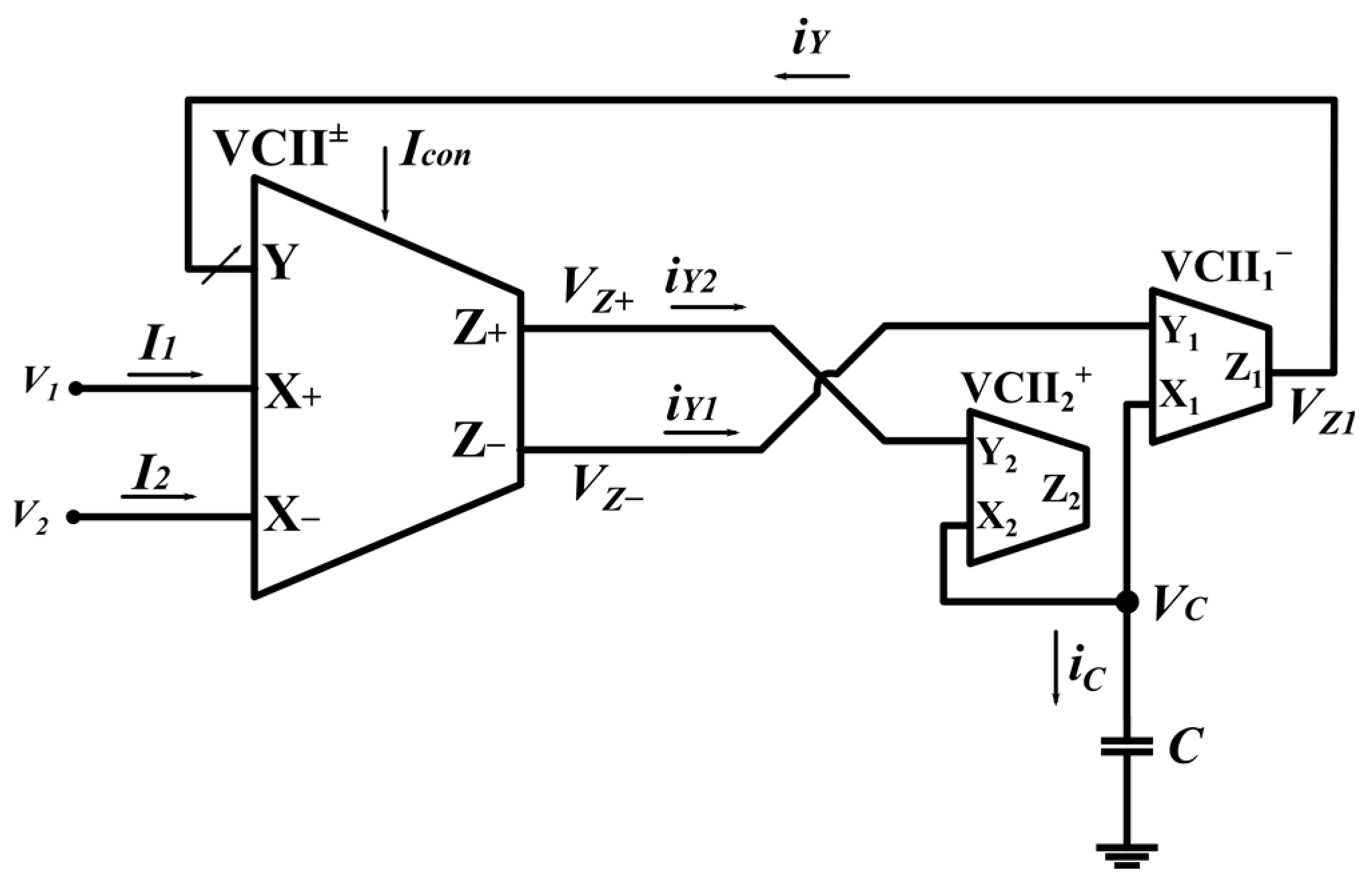
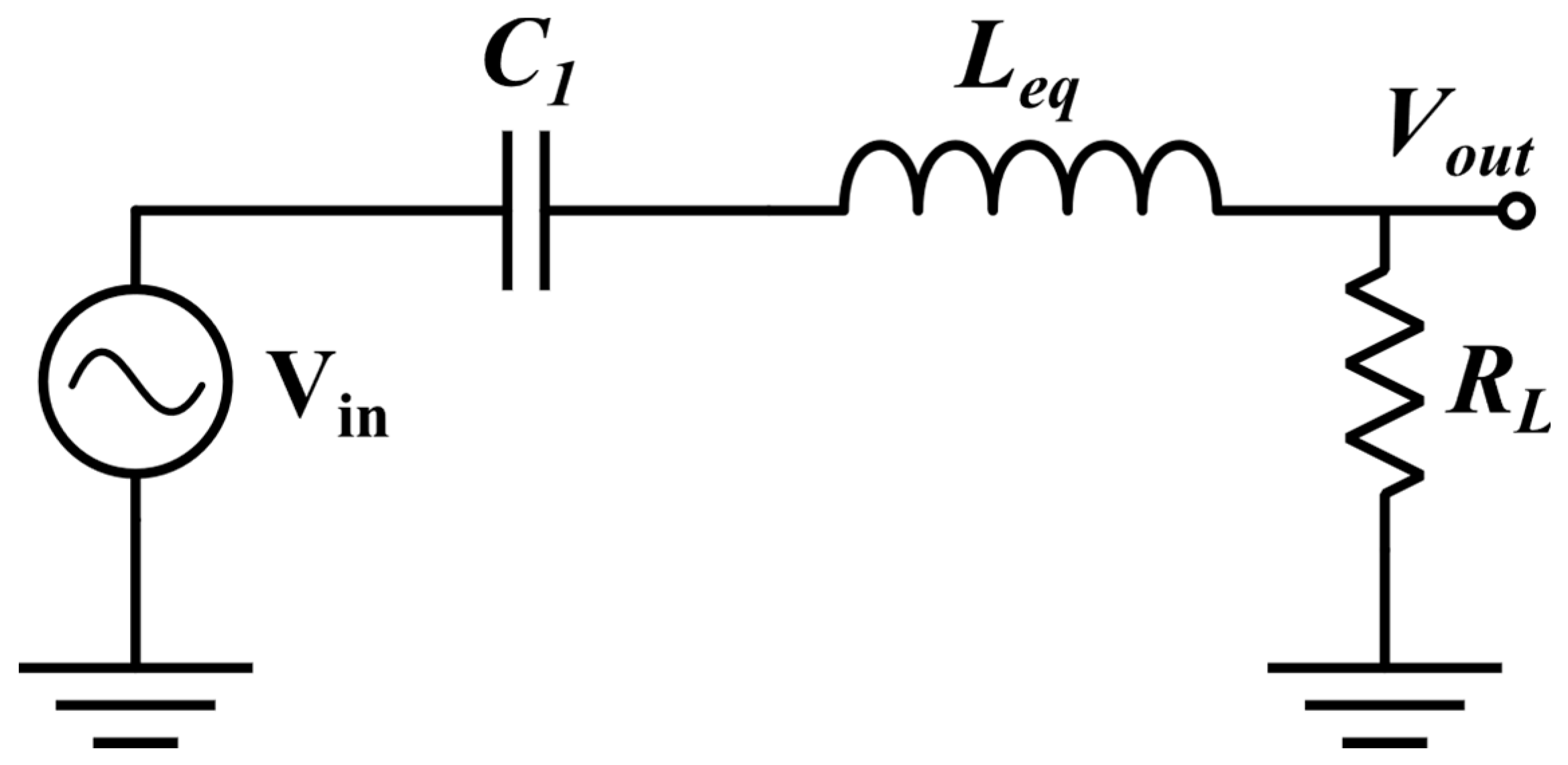
2. The Proposed VCII Based Floating Inductance Simulator
The proposed VCII-based floating capacitor simulator is shown in Figure 1. It is composed of one VCII±, one VCII+, one VCII− and a grounded capacitor. The operation of VCII+ and VCII− is expressed by the matrix Equation (1) as follows:
Figure 1.
The proposed floating positive capacitance simulator.
In (1), β is the current gain between the Y and X terminals while α is the voltage gain between then X and Z terminals. Here, +β and −β indicate VCII+ and VCII−, respectively. In the ideal case, the values of β and α are unity. The parameters rx, rz and rY are parasitic impedances at the X, Z and Y terminals, respectively. In the ideal case, rx and rz are infinite and zero, respectively, while Cx (with ideal value of zero) represents the parasitic capacitance at the X terminal. To eliminate the need for passive resistors, we take advantage of the parasitic impedance at the Y terminals of VCII+ and VCII-. For the used VCIIs, the value of rY is designed at a constant non-zero value, while the value of rY in VCII± is varied using a control current resulting in electronic tunability for the simulated inductor. This property is shown as a small arrow on the Y terminal of VCII±. The performance of VCII± with electronically variable impedance at the Y terminal is shown in the matrix (2):
In (2), the current gain between Y and X+ are shown by β+ while the one between Y and X− are shown by −β− with ideal values of unity. The voltage gain between the X+ and Z+ terminals is shown by α+ and the voltage gain between the X− and Z− terminals is shown by α− with ideal values of unity. Here, rx+, rx−, rz+ and rz− are parasitic impedances at the X+, X−, Z+ and Z− terminals, respectively, with ideal values of infinite, infinite, zero and zero, respectively. The parasitic resistor rY is designed at a non-zero value which can be electronically varied through Icon. In (1) and (2), the parasitic capacitors at the X terminals are shown by Cx+ and Cx− which have ideal values of zero.
In the ideal case analysis, the values of β and α are assumed to be unitary. The parasitic impedances at the X and Z ports are assumed as infinite and zero, respectively. The values of the Y port impedances are shown by rY1, rY2 and rY for VCII−1, VCII+2 and VCII±, respectively.
By these assumptions, the operation of the proposed circuit of Figure 1 can be analyzed as follows. Using (2) for VZ+ and VZ− we have:
where V1 and V2 are input voltages. At the Y terminals of VCII−1 and VCII+2, proportional currents are produced through rY1 and rY2 as:
Using (1), (4) and (5), the current produced at C is found as:
By assuming rY1 = rY2 = r, from (6), VC is found as:
From (2), VC is transferred to the Z1 terminal where it is converted to a proportional current through the Y terminal impedance of VCII± as:
where rY is the electronically variable impedance at the Y terminal of VCII±. From (8), the value of the simulated inductor is found as:
To achieve negative impedance values, we need to change the connection of the Z terminals of VCII± and the Y terminals of VCII−1 and VCII+2, as shown in Figure 2. Similarly, it can be shown that the simulated inductor of Figure 2 is:
Figure 2.
The proposed floating negative inductor simulator.
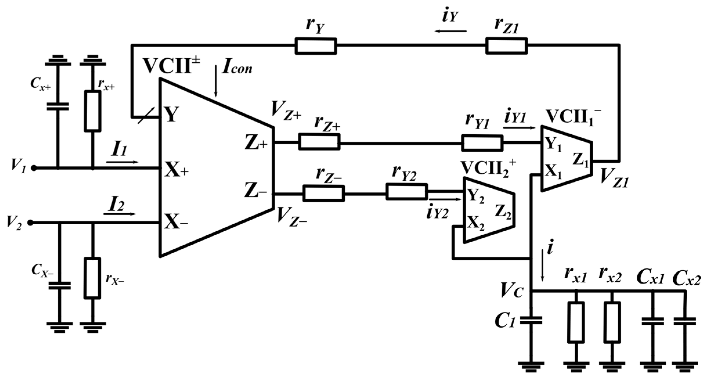
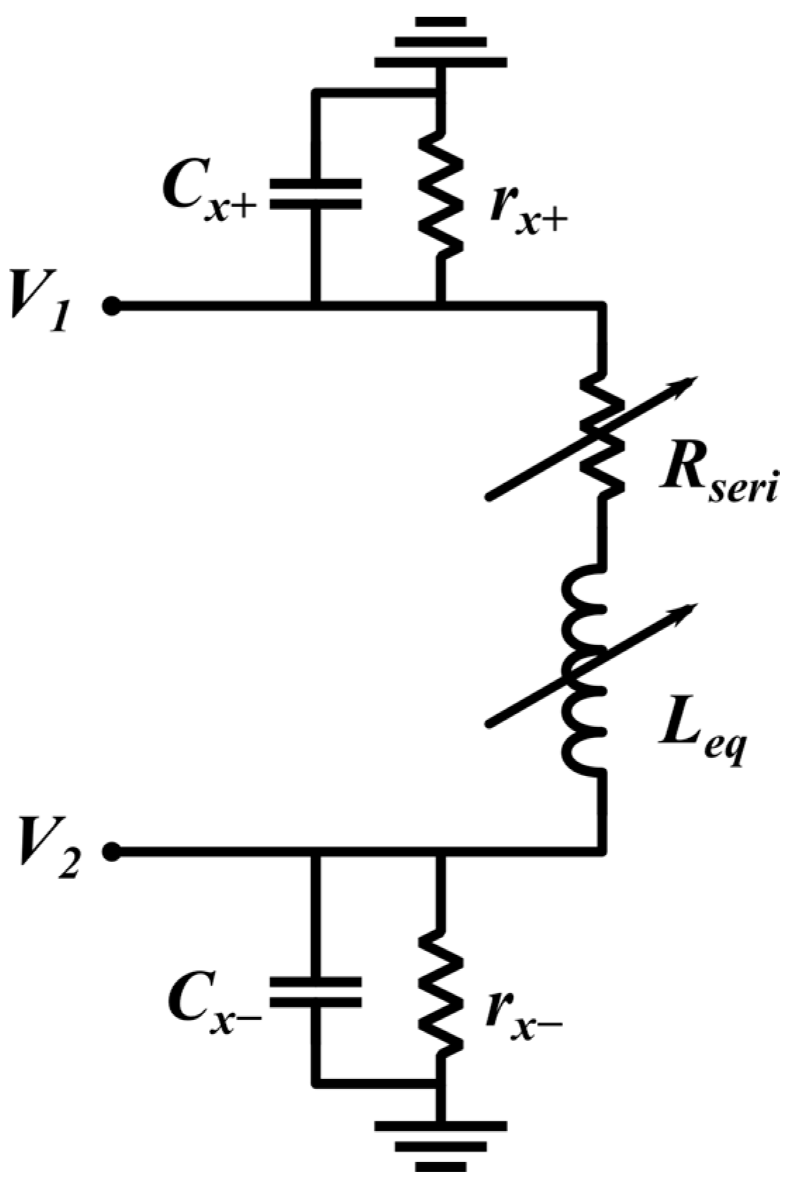
3. Non-Ideal Analysis
Figure 3 shows the proposed inductor simulator topology in which all parasitic elements of the used ABBs are shown. A complete non-ideal analysis of the proposed circuit can be performed as follows.
Figure 3.
The floating inductor simulator with parasitic elements.
Using (1) and performing a simple analysis using the Kirchhoff current and voltage laws (KCL, KVL) iY1 and iY2 are found as:
Again using (1) and performing a KCL analysis, VC is found as:
where:
Inserting (11) and (12) into (13) results in:
Using (1), (2) and (16), iY is found as:
From the matrix equation of (2), by ignoring the effect of rx+ and rx−, I1 and I2 are:
Assuming (rZ+ + rY1) = (rZ− + rY2) = r′ and (rZ1 + rY) = r″, (18) and (19) become:
By defining the voltage gain and current gain parameters of the used VCII as:
where ε << 1, ε′ << 1 and ε″ << 1 are gain errors, and inserting (22)–(27) into (20) and (21) and simplifying the results gives:
From (28), (29) Leq and its series impedance Rseri are found as:
As can be seen from (30), the value of Leq can be varied by rY. From (14) and (31), it is also deduced that as the value of req is much larger than rY1, rY2 and rY, the value of Rseri is low. The equivalent circuit of the proposed capacitor simulator is shown in Figure 4, where Leq is the proposed electronically tunable equivalent floating inductor. rx and Cx are the parasitic parallel resistance and capacitance and Rseri is the parasitic series resistance of the simulated inductor. Similar analysis can be performed for the negative inductance simulator which is not repeated here.
Figure 4.
The equivalent circuit of the proposed floating L simulator.
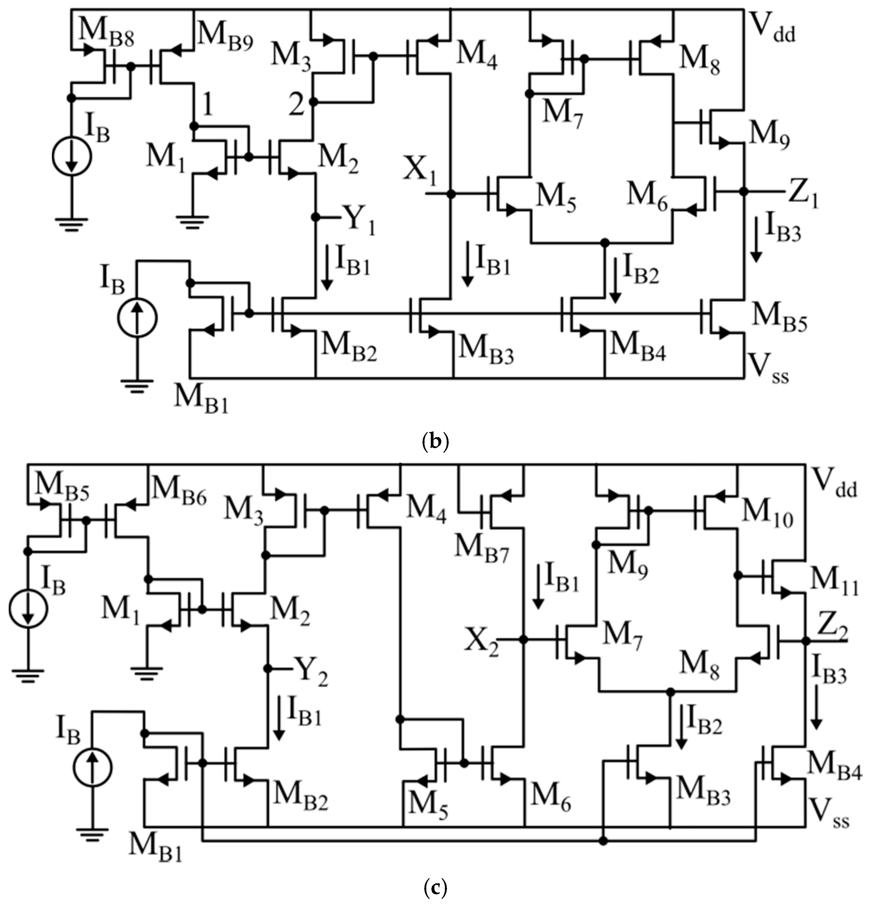
4. CMOS Implementation of VCII
A simple realization of the internal structure of VCII± is shown in Figure 5a. The input section at the Y port is composed of transistors M1 and M2, Icon, IB1 and IB2. Transistor M2 is used in common gate structure and the bias voltage at its gate is provided by diode connected transistor M1. The impedance at the Y terminal is:
where gmM2 (with usual meaning of symbols) is:

Figure 5.
CMOS implementation of (a) electronically controllable VCII±, (b) VCII+ and (c) VCII−.
From (33), by increasing the value of Icon, the value of gmM2 will be increased and according to (32), the value of rY will be reduced. To reduce power consumption, Icon is added to the drain of M2 to keep the bias current at other branches constant. To set the zero-offset voltage at Y port, Icon is also added to the drain of M1. This is performed by transistors MB11-MB16.
The input current applied to the Y terminal is transferred to the X+ terminal through a simple current mirror made of M3 and M4. On the other hand, the input current at the Y terminal is transferred to the X− terminal by transistors M3, M4, M10–M12. The voltage produced at the X+ terminal is transferred to the Z+ terminal through a voltage buffer made of M5–M9. Similarly, the voltage produced at the X− terminal is transferred to the Z− terminal through a voltage buffer of M14–M18. Transistors MBi for i = 1–10 are used for biasing. A simple analysis gives the parasitic elements at the X+, X− Z+ and Z− terminals as:
where for ith transistor, roMi is the drain-source impedance, gmMi is the transconductance and roMBi is the drain source impedance and CdsMi and CdgMi are the drain-source capacitance and drain-gate capacitance of the related transistor.
The implementation of the VCII+ and the VCII− are shown in Figure 5b,c, respectively. Here, transistor M2 is configured in a common gate structure and the diode connected transistor M1 provides proper biasing at the gate of M1. A simple current mirror made of M3 and M4 in Figure 5b, and current mirrors made of M3 and M4, and M5 and M6 in Figure 5c, are used to transfer the Y port input current to the X ports. The voltage produced at the X ports is transferred to the Z ports by a voltage buffer made of M5–M9 in Figure 5b and M7–M11 in Figure 5c.
Parasitic elements are found as:
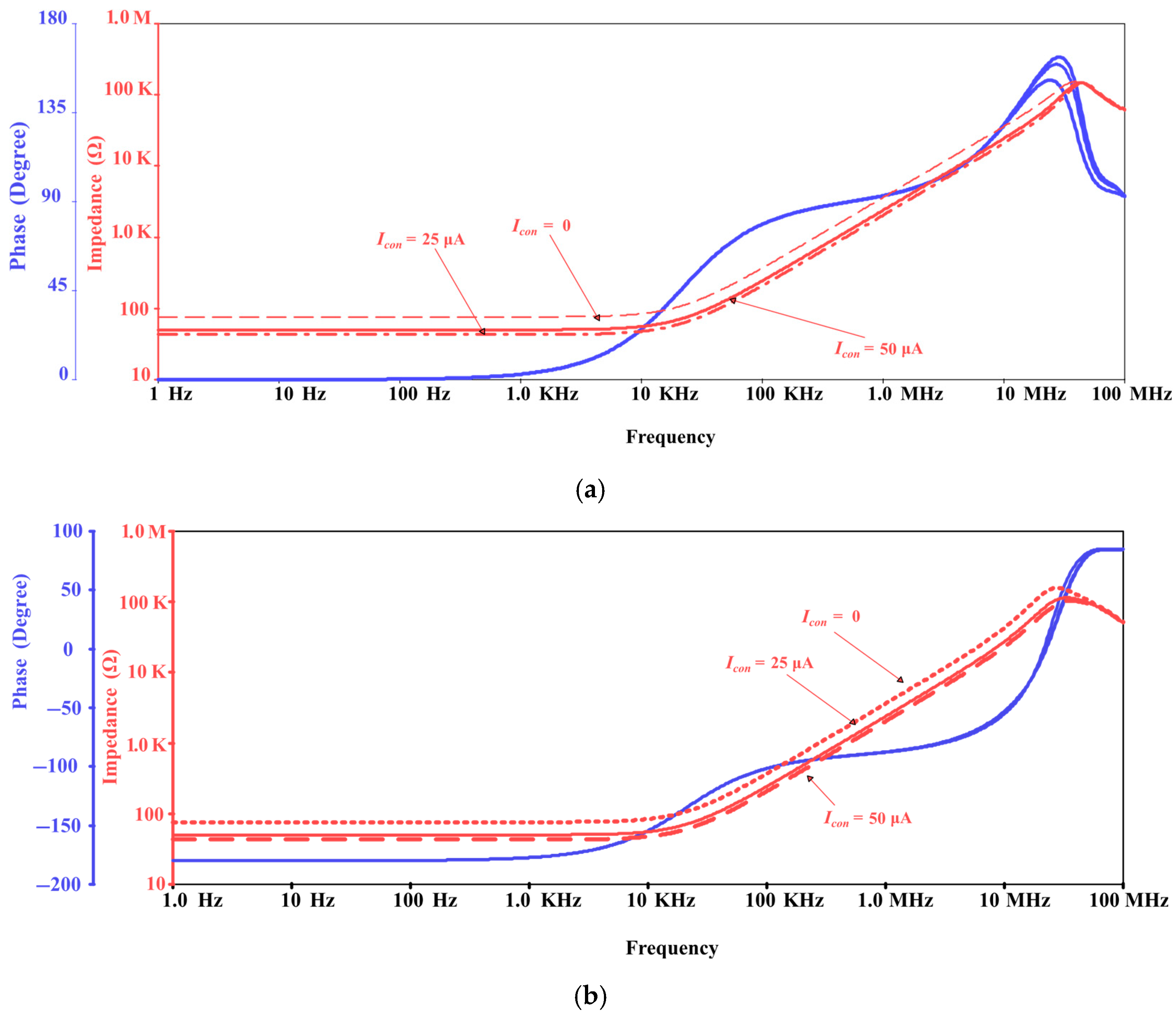
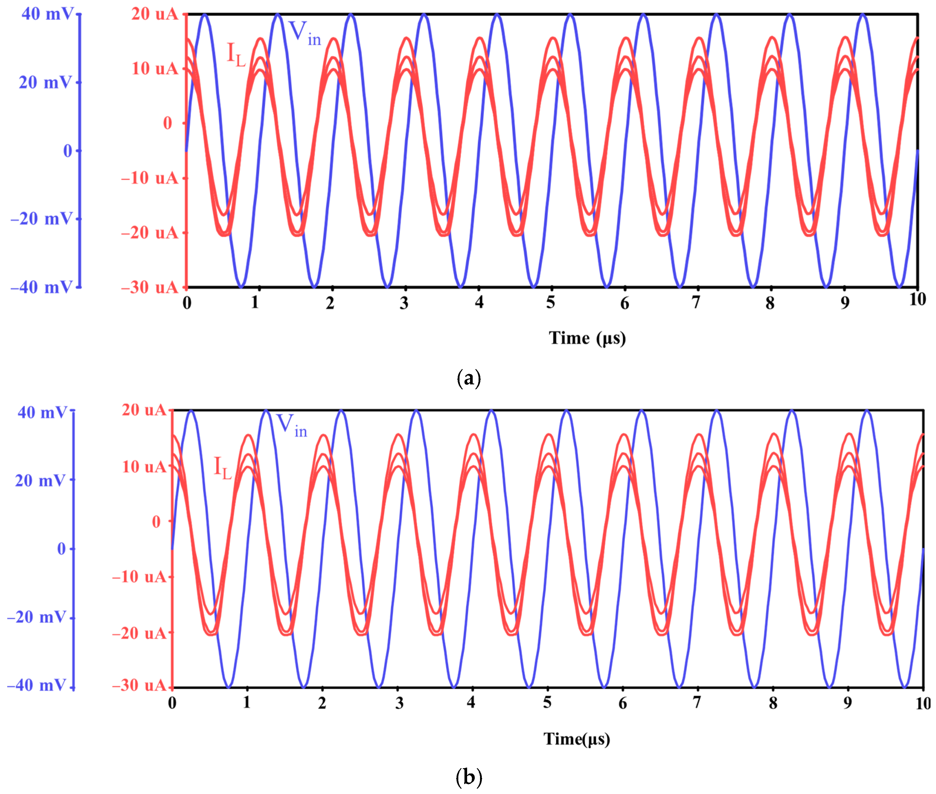
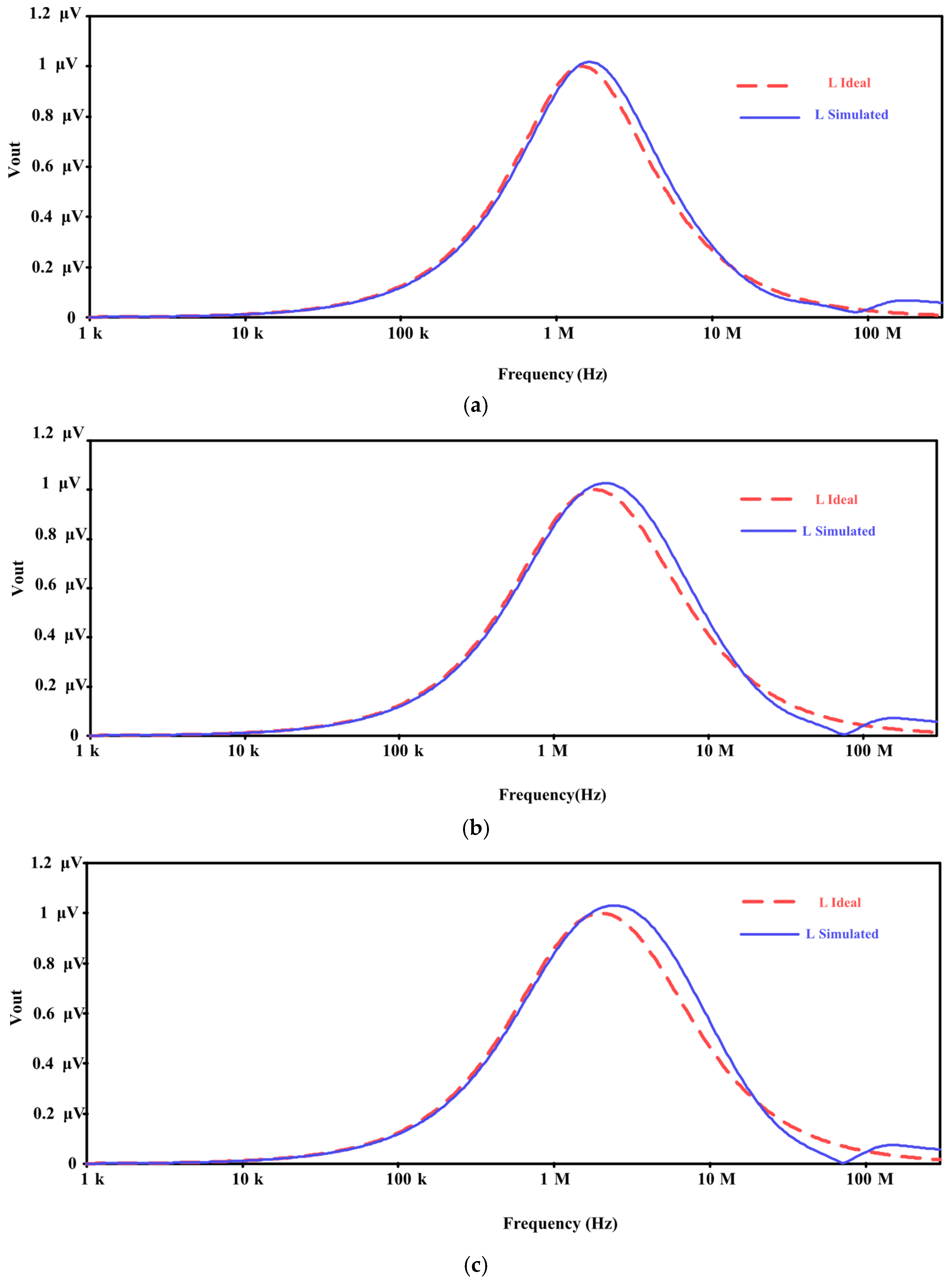
5. Simulation Results
PSpice simulations of the proposed floating inductors of Figure 1 and Figure 2 based on 0.18 μm CMOS technology and supply voltage of ±0.9 V are performed. The aspect ratios for the used PMOS and NMOS transistors are 9 µm/0.9 µm and 27 µm/0.9 µm, respectively. The values of the bias currents are IB = IB1 = IB2 = IB3 = 20 µA. All bias currents are realized by simple current mirrors. The performance parameters and parasitic elements of the used ABBs are reported in Table 1.
Table 1.
The simulated characteristics of VCII±, VCII+ and VCII−.
For C1 = 50 pF, Figure 6 shows the phase and magnitude frequency response of the proposed floating inductor for Icon = 0 µA, Icon = 25 µA and Icon = 50 µA. The proposed circuit frequency range is from 100 kHz to 3 MHz.
Figure 6.
Frequency response of magnitude and phase for the proposed (a) positive and (b) negative floating inductor simulator.
Table 2 shows the value of the achieved inductance for different values of Icon for both theoretical and simulated values. As can be seen, the error for Leq remains below 4.8%. Fortunately, the maximum value of Rseri remains at 76 Ω.
Table 2.
Deviation between theoretical and ideal values at different control currents.
To test the time domain response of the proposed inductor simulator, a sinusoidal input voltage with a peak-to-peak value of 80 mV and frequency of 1 MHz is used as the input signal to the simulated inductor. The output signal phase is 93.6° and −86.4° for positive and negative types, respectively. The resulting outputs are shown in Figure 7.
Figure 7.
Time domain response of the proposed (a) positive and (b) negative floating inductors.
The functionality of the proposed floating inductor is tested on a standard RLC band-pass filter for C1 = 50 pF, RL = 10 kΩ shown in Figure 8. Figure 9 shows the frequency response of the RLC band-pass filter for both the ideal and the simulated inductance. The simulated value of f0 is 1.04 MHz, 1.39 MHz and 2.39 MHz for Icon = 0 µA, Icon = 25 µA and Icon = 50 µA, respectively.
Figure 8.
Application of simulated Floating L as a RLC band-pass filter.
Figure 9.
Frequency response of the RLC band-pass filter for different values of Icon (a) 0 µA (b) 25 µA and (c) 50 µA.
The robustness of the design was tested as well. In particular, Table 3, Table 4 and Table 5 show the PVT variations of the VCII±, VCII+ and VCII− ABBs, respectively, while in Table 6, the same variations are tested for the actual equivalent inductor value. Simulations have been reported at different Icon levels. Results show that, regardless of the conditions, values always remain within 3% of the nominal ones reported along the manuscript concerning the ABBs parameters, while they remain within 11% when it comes to the equivalent inductor value.
Table 3.
PVT simulation results for VCII±.
Table 4.
PVT simulation results for VCII+.
Table 5.
PVT simulation results for VCII−.
Table 6.
PVT simulation results for the achieved Leq at different control currents.
Monte Carlo simulations have been performed and reported in Table 7 as well. They have been conducted emulating a 1% mismatch in the β parameter with an overall of 50 runs. As can be seen, the spread between minimum and maximum value increases as the control current reduces. This is expected and depends on the fact that the error from the mirroring action of the current mirrors is more relevant at a low bias current. It could be mitigated, for instance, using cascaded structures if the voltage swing is not a strong issue.
Table 7.
Monte Carlo for 1% mismatch in β and 50 runs.
A comparison between the proposed circuit and other previously reported ones is presented in Table 8. As can be seen, compared to other works, the proposed circuit provides full integration as it is resistor-free and uses only one grounded capacitor. Although the circuit reported in [11] is also resistor-free, it includes a floating compensation capacitor inside the used OA. Moreover, the proposed floating inductor can provide both positive (+L) and negative (−L) inductance values. Although the circuits reported in [5,6] are electronically tunable, the large number of capacitors and resistors which their values must trim is their weakness. The circuits reported in [7,8,10,11] are electronically tunable but they can provide only +L. The circuits reported in [9,12,13,14,15] are not electronically tunable.
Table 8.
Comparison between proposed circuit and other reported works.
6. Conclusions
In this paper, we present a new topology for implementing either a positive or negative floating inductor multiplier. One VCII±, one VCII+, one VCII− and a single grounded capacitor are used. Instead of passive resistors, intrinsic resistors at the Y terminals of VCIIs are used. The value of the simulated inductor is tunable by a control current. The circuit enjoys low voltage and low power operation, reduced series resistance and offers fewer errors compared to other works. Non-ideal analysis is given by taking into account the non-ideal gains and parasitic impedances of the active elements that are used. The proposed circuit enjoys a simple implementation and is free from any restricting matching requirements. The application of the proposed circuit as a standard RLC filter is also given to verify its functionality.
Author Contributions
Editing, L.S., G.F. and V.S.; visualization, G.B., D.C. and L.S.; supervision, G.F. and V.S.; project administration, G.F. and V.S.; funding acquisition, G.F. and V.S. All authors have read and agreed to the published version of the manuscript.
Funding
This work was supported in part by the Italian Ministry of Education, University and Research (MIUR) with the research grant “ASSIOMI”, “PON R&I 2014–2020”.
Data Availability Statement
Data sharing not applicable. No new data were created or analyzed in this study. Data sharing is not applicable to this article.
Conflicts of Interest
The authors declare no conflict of interest.
References
- Ye, X.; Wang, Y.; Tang, X.-Y.; Ji, H.; Wang, B.; Huang, Z. On the Design of a New Simulated Inductor Using a Contactless Electrical Tomography System as an Example. Sensors 2019, 19, 2463. [Google Scholar] [CrossRef] [Green Version]
- Lyu, Y.; Huang, J.; Huang, Z.; Ji, H.; Wang, B.; Li, H. Study on the application of simulated inductor technique to the design of C4D sensor. Sens. Actuators A Phys. 2017, 264, 195–204. [Google Scholar] [CrossRef]
- Soliman, A. On the realization of floating inductors. Nat. Sci. 2010, 8, 167–180. [Google Scholar]
- Reddy, M. Some new operational-amplifier circuits for the realization of the lossless floating inductance. IEEE Trans. Circuits Syst. 1976, 23, 171–173. [Google Scholar] [CrossRef]
- Said, L.A.; Madian, A.H.; Ismail, M.H.; Soliman, A.M. Digitally programmable lossless floating inductor realization using current differential amplifier (CDA). In Proceedings of the 16th IEEE Mediterranean Electrotechnical Conference, Yasmine Hammamet, Tunisia, 25–28 March 2012; IEEE: Piscataway, NJ, USA, 2012; pp. 840–843. [Google Scholar]
- Said, L.A.; Madian, A.H.; Isamil, M.H.; Soliman, A.M. CMOS digitally programmable lossless floating inductor. In Proceedings of the IEEE International Conference of Electron Devices and Solid-State Circuits (EDSSC), Hong Kong, China, 15–17 December 2010; IEEE: Piscataway, NJ, USA, 2010; pp. 1–4. [Google Scholar]
- Bhaskar, D.R.; Prasad, D.; Singh, A.K. New Grounded and Floating Simulated Inductance Circuits using Current Differencing Transconductance Amplifiers. Radio Eng. 2010, 19, 194–198. [Google Scholar]
- Tangsrirat, W. Floating simulator with a single DVCCTA. Indian J. Eng. Mater. Sci. 2013, 20, 79–86. [Google Scholar]
- Ibrahim, M.A.; Minaei, S.; Yuce, E.; Herencsar, N.; Koton, J. Lossy/lossless floating / grounded inductance simulation using one DDCC. Radioengineering 2012, 21, 3–10. [Google Scholar]
- Zhou, X.; Zeng, R. Floating Inductance Simulators Based on Active Components. DEStech Trans. Eng. Technol. Res. 2017, 1904–1908. [Google Scholar] [CrossRef] [Green Version]
- Lawanwisut, S.; Siripruchyanun, M. An electronically controllable active-only current-mode floating inductance simulator. In Proceedings of the 35th International Conference on Telecommunications and Signal Processing (TSP), Prague, Czech Republic, 3–4 July 2012; IEEE: Piscataway, NJ, USA, 2012; pp. 386–389. [Google Scholar]
- Yuce, E.; Tokat, S.; Alpaslan, H. Grounded capacitor-based new floating inductor simulators and a stability test. Turk. J. Electr. Eng. Comput. Sci. 2015, 23, 2138–2149. [Google Scholar] [CrossRef] [Green Version]
- Likhitkitwoerakul, N.; Roongmuanpha, N.; Tangsrirat, W. Floating Impedance Simulator Realization. In Proceedings of the 17th International Conference on Electrical Engineering/Electronics, Computer, Telecommunications and Information Technology (ECTI-CON), Phuket, Thailand, 24–27 June 2020; IEEE: Piscataway, NJ, USA, 2020; pp. 345–348. [Google Scholar]
- Yuce, E.; Minaei, S. A Modified CFOA and Its Applications to Simulated Inductors, Capacitance Multipliers, and Analog Filters. IEEE Trans. Circuits Syst. I Regul. Pap. 2008, 55, 266–275. [Google Scholar] [CrossRef]
- Al-Absi, M.A. Realization of a Large Values Floating and Tunable Active Inductor. IEEE Access 2019, 7, 42609–42613. [Google Scholar] [CrossRef]
- Čajka, J.; Vrba, K. The Voltage Conveyor May Have in Fact Found its Way into Circuit Theory. AEU Int. J. Electron. Commun. 2004, 58, 244–248. [Google Scholar] [CrossRef]
- Safari, L.; Barile, G.; Stornelli, V.; Ferri, G. An Overview on the Second Generation Voltage Conveyor: Features, Design and Applications. IEEE Trans. Circuits Syst. II Express Briefs 2019, 66, 547–551. [Google Scholar] [CrossRef]
- Safari, L.; Barile, G.; Ferri, G.; Stornelli, V. High performance voltage output filter realizations using second generation voltage conveyor. Int. J. RF Microw. Comput. Aided Eng. 2018, 28, e21534. [Google Scholar] [CrossRef]
- Safari, L.; Barile, G.; Ferri, G.; Stornelli, V. Traditional Op-Amp and new VCII: A comparison on analog circuits applications. AEU Int. J. Electron. Commun. 2019, 110, 152845. [Google Scholar] [CrossRef]
- Safari, L.; Barile, G.; Stornelli, V.; Ferri, G.; Leoni, A. New Current Mode Wheatstone Bridge Topologies with Intrinsic Linearity. In Proceedings of the 14th Conference on Ph.D. Research in Microelectronics and Electronics (PRIME), Prague, Czech Republic, 2–5 July 2018; IEEE: Piscataway, NJ, USA, 2018; pp. 9–12. [Google Scholar]
- Stornelli, V.; Safari, L.; Barile, G.; Ferri, G. A New Extremely Low Power Temperature Insensitive Electronically Tunable VCII-Based Grounded Capacitance Multiplier. IEEE Trans. Circuits Syst. II Express Briefs 2021, 68, 72–76. [Google Scholar] [CrossRef]
- Safari, L.; Yuce, E.; Minaei, S.; Ferri, G.; Stornelli, V. A second-generation voltage conveyor (VCII)–based simulated grounded inductor. Int. J. Circuit Theory Appl. 2020, 48, 1180–1193. [Google Scholar] [CrossRef]
Publisher’s Note: MDPI stays neutral with regard to jurisdictional claims in published maps and institutional affiliations. |
© 2022 by the authors. Licensee MDPI, Basel, Switzerland. This article is an open access article distributed under the terms and conditions of the Creative Commons Attribution (CC BY) license (https://creativecommons.org/licenses/by/4.0/).