
A 5.42~6.28 GHz Type-II PLL with Dead-Zone Programmability and Charge Pump Mismatch Trimming

Abstract
:1. Introduction
2. PLL Designs
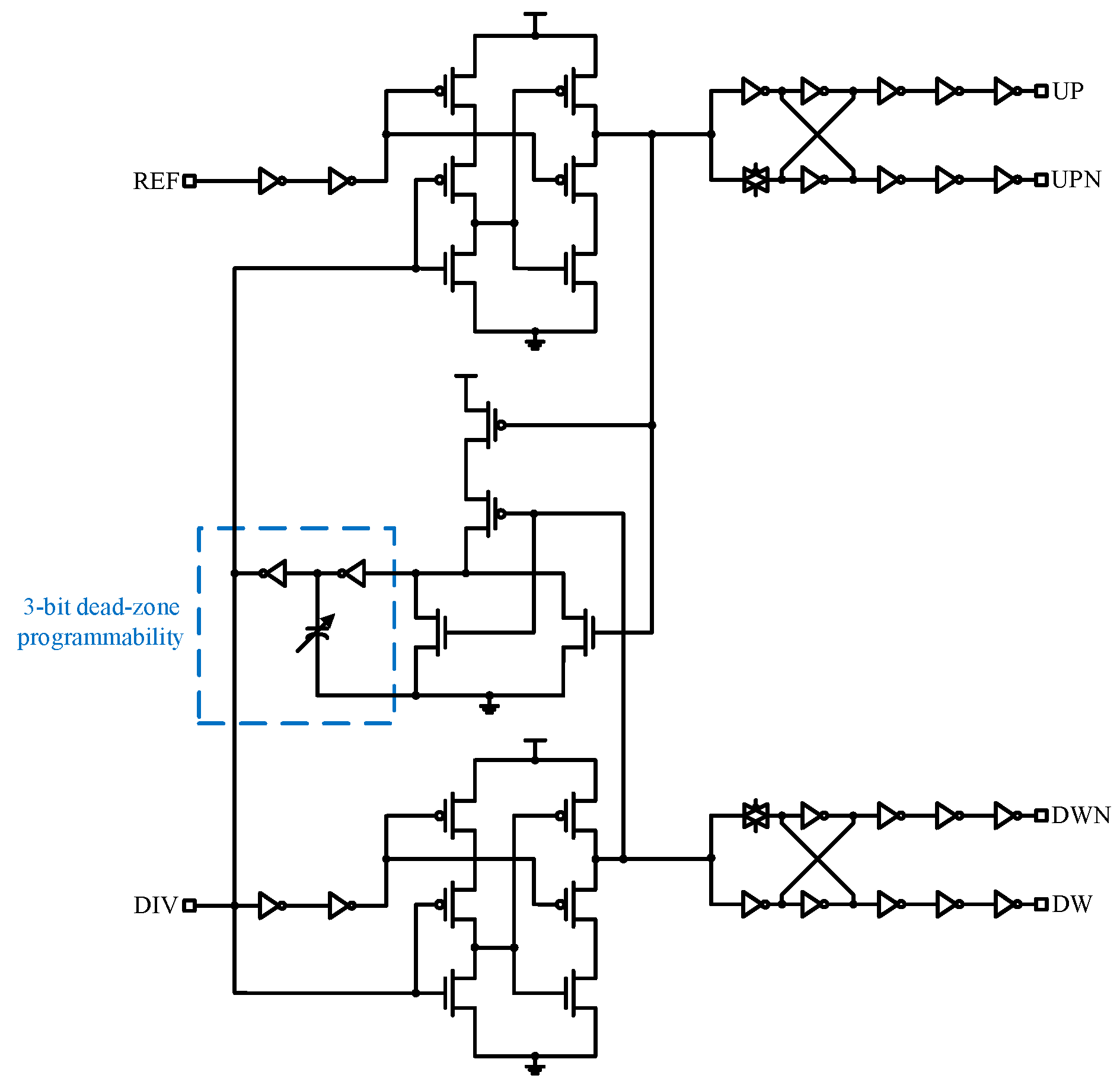
2.1. PFD Topology
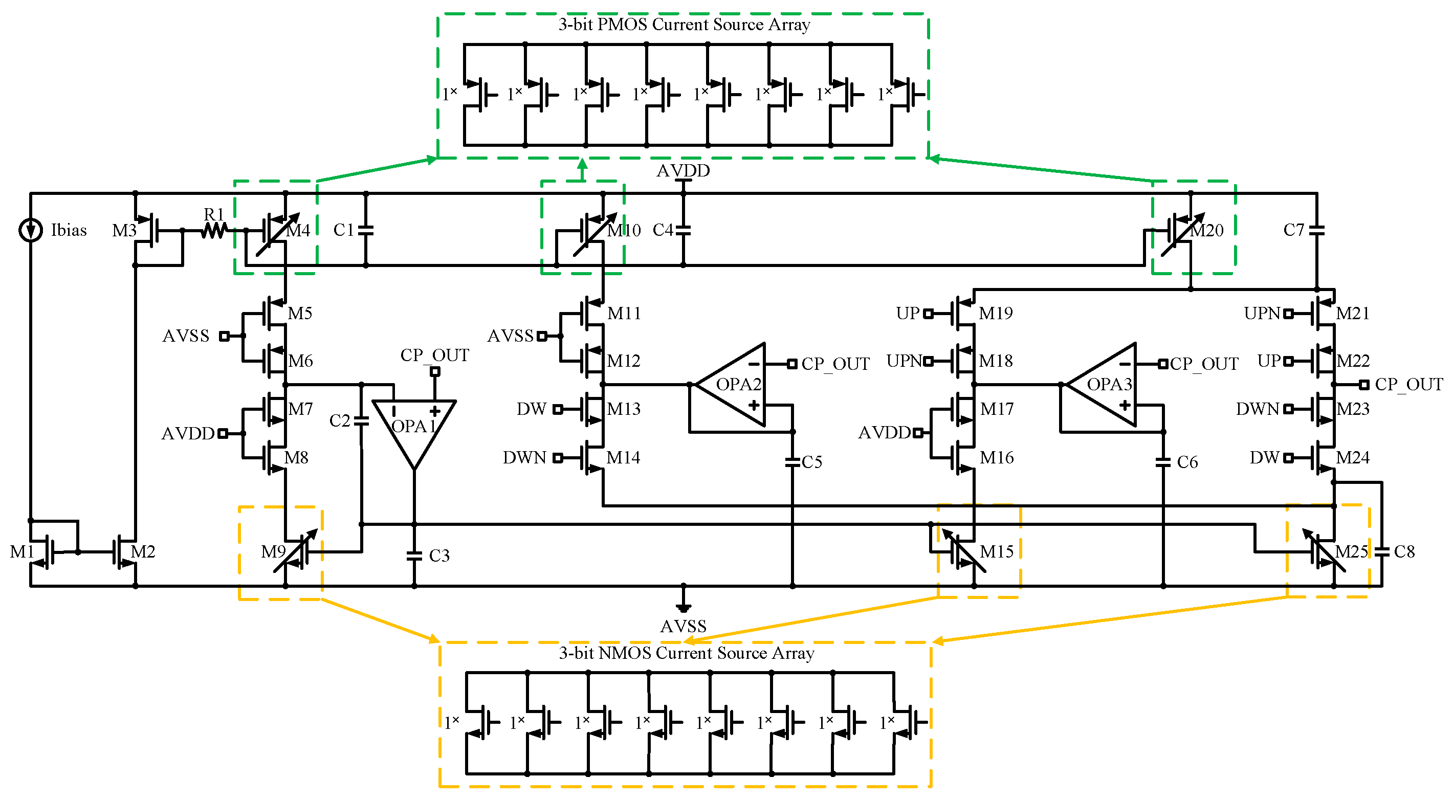
2.2. CP Topology
2.3. Divider Chain Topology
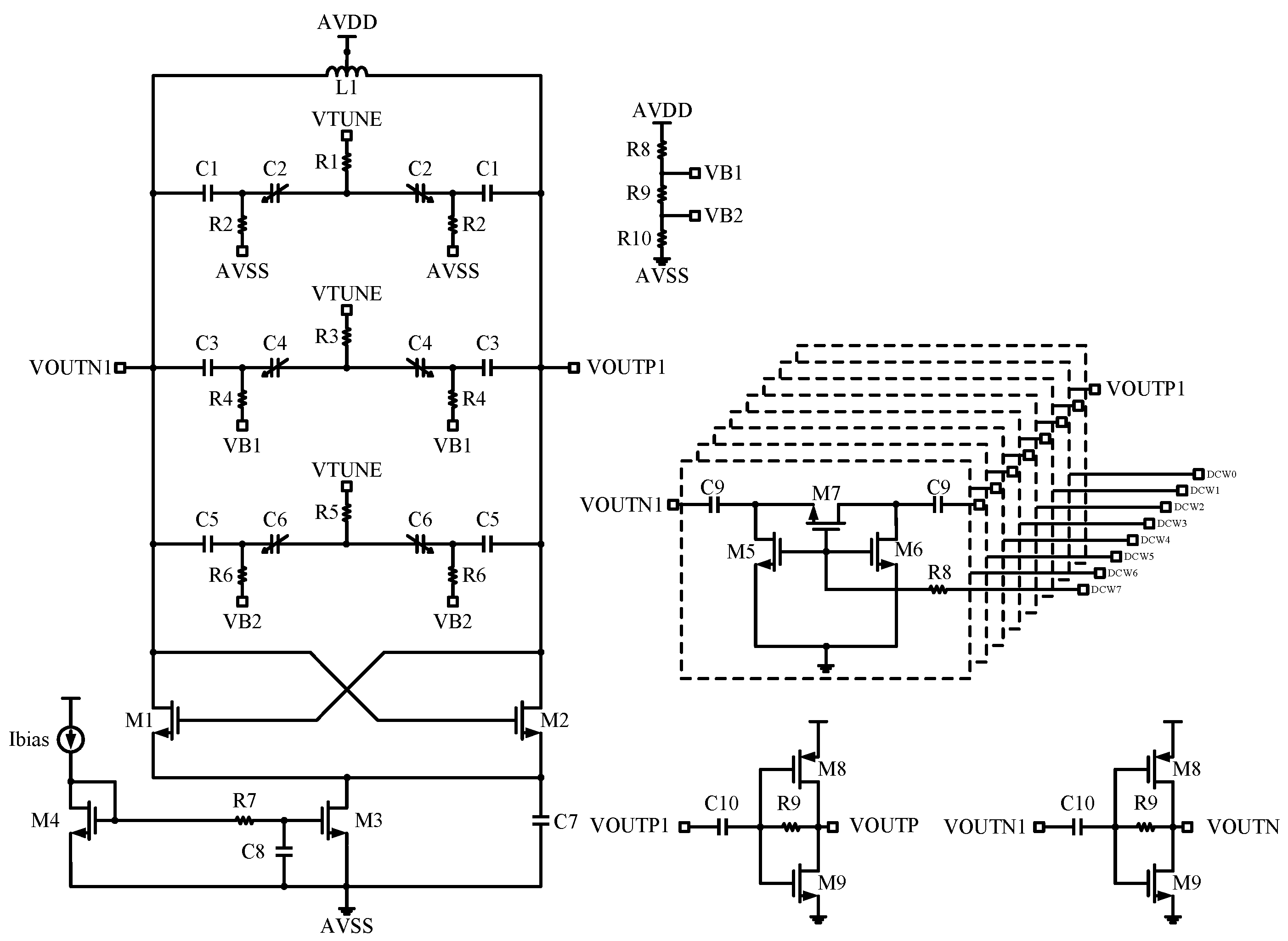
2.4. VCO Topology
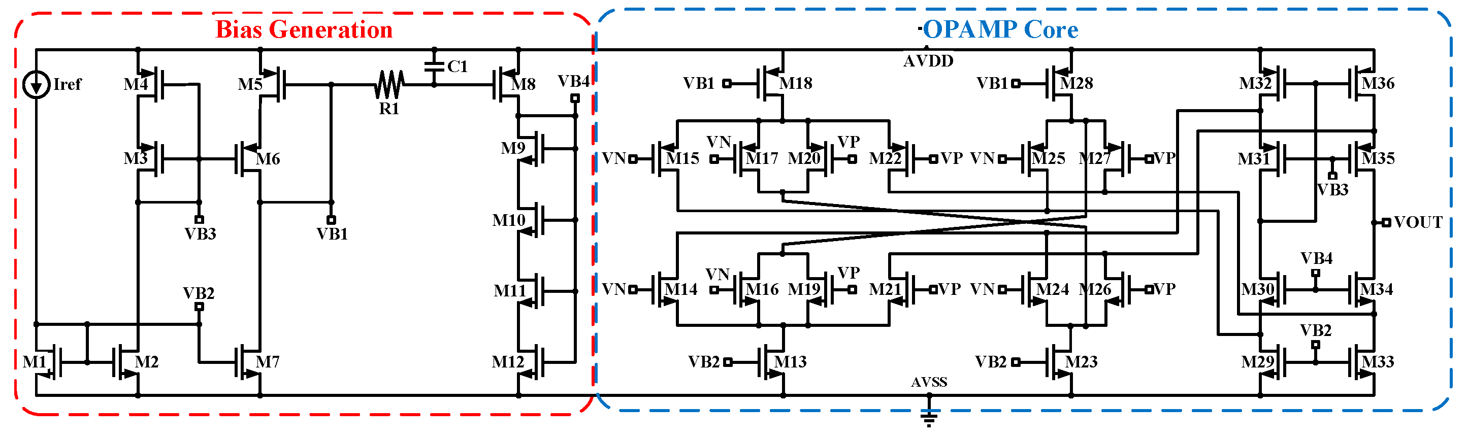
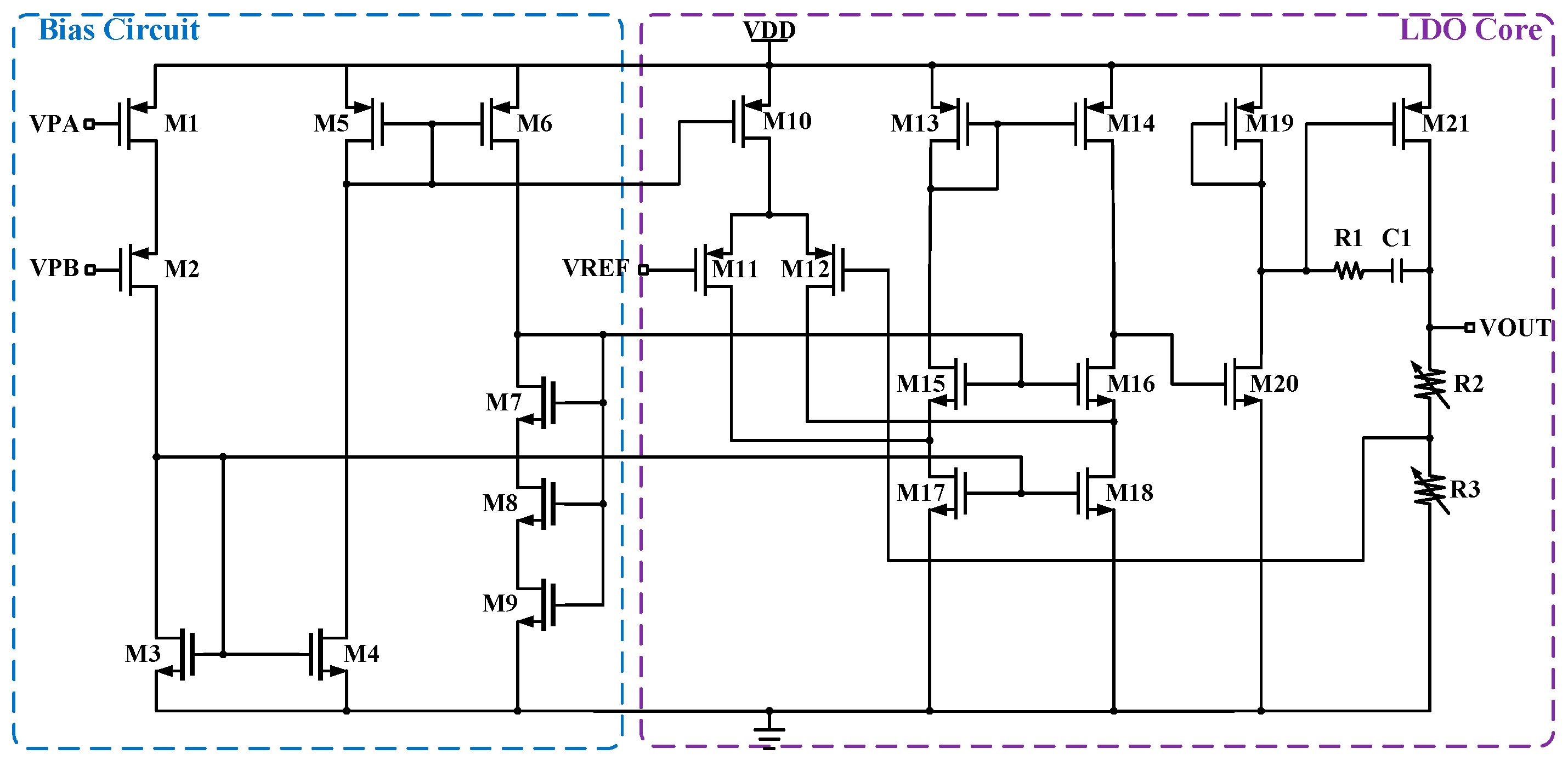
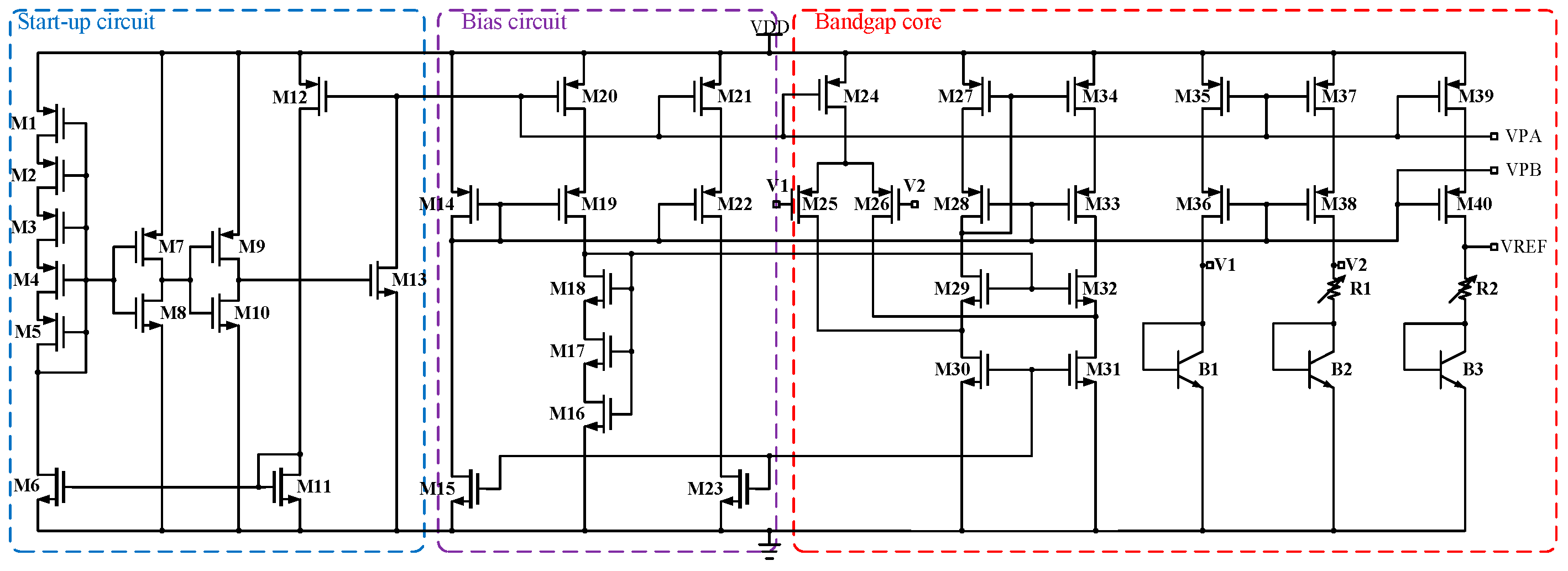
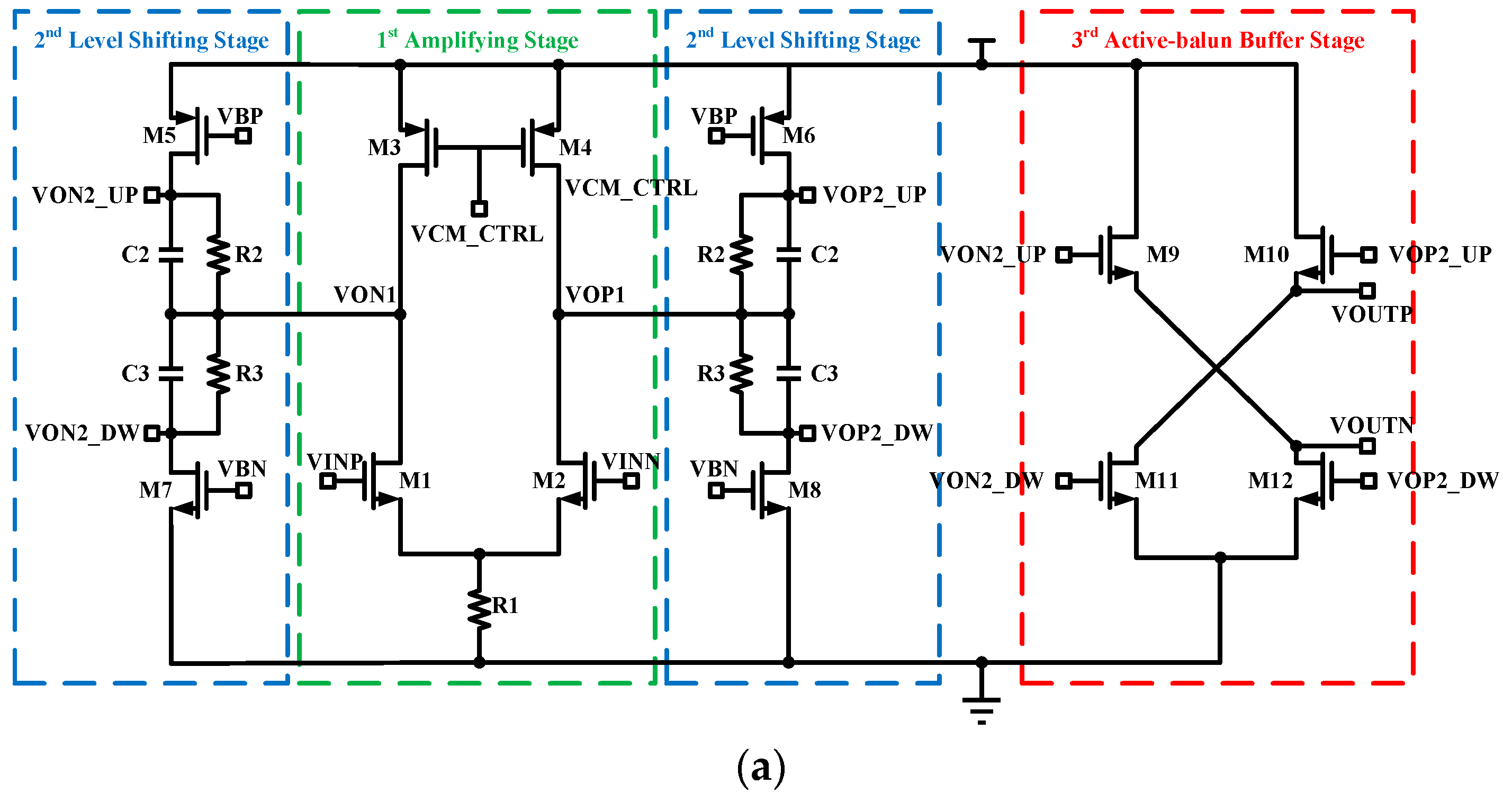
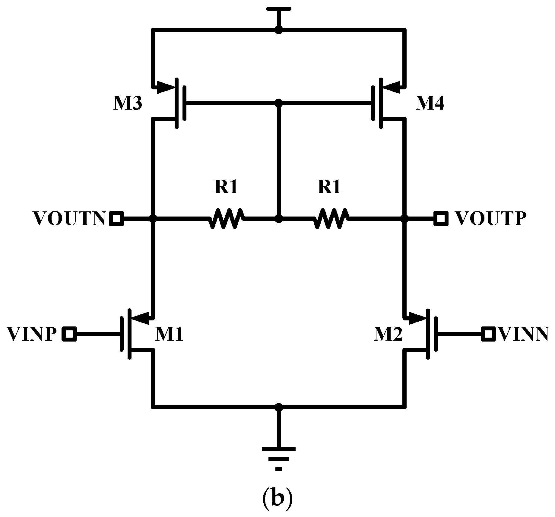
2.5. PMU Topology
2.6. Loop Filter Topology
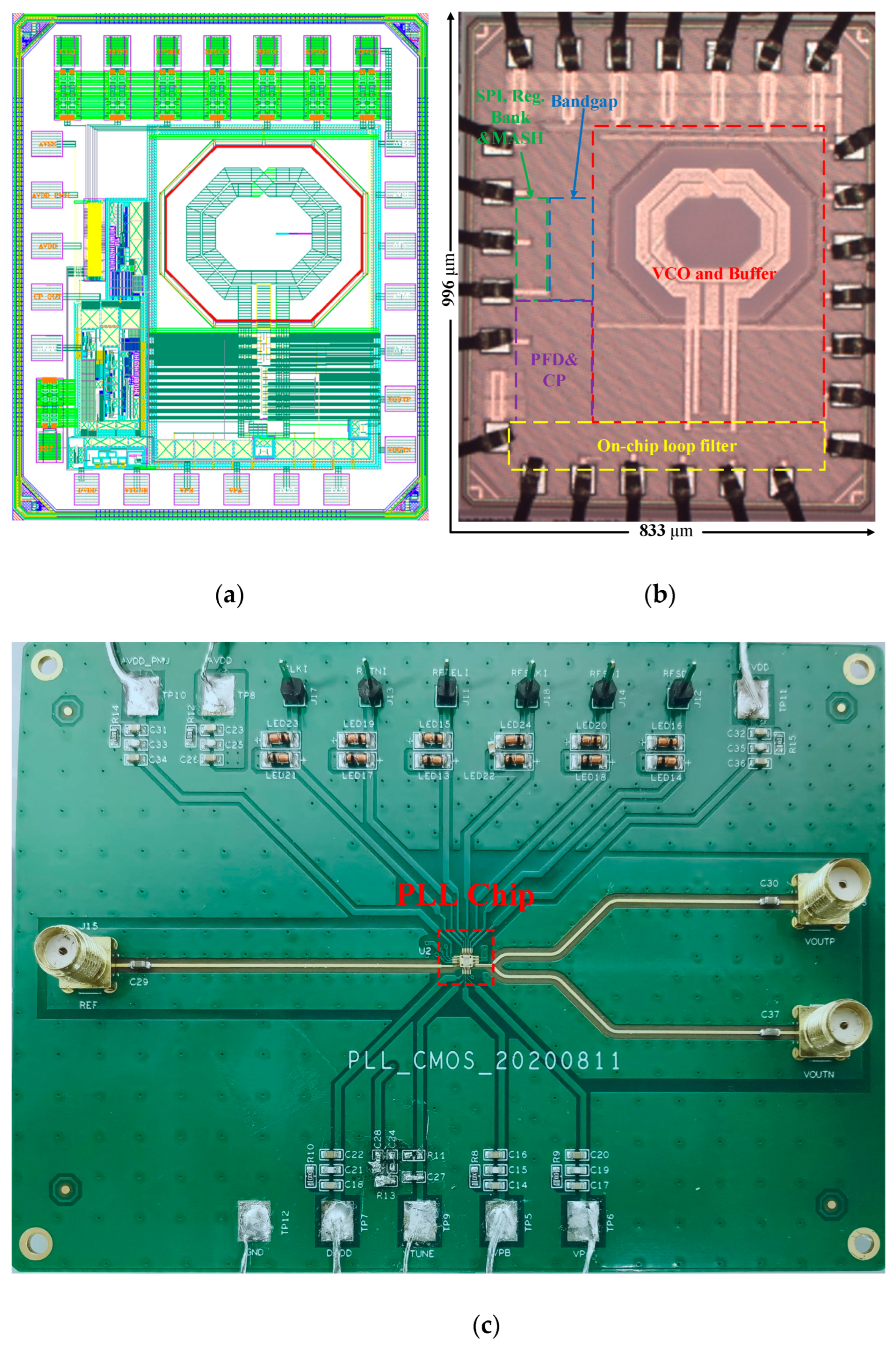
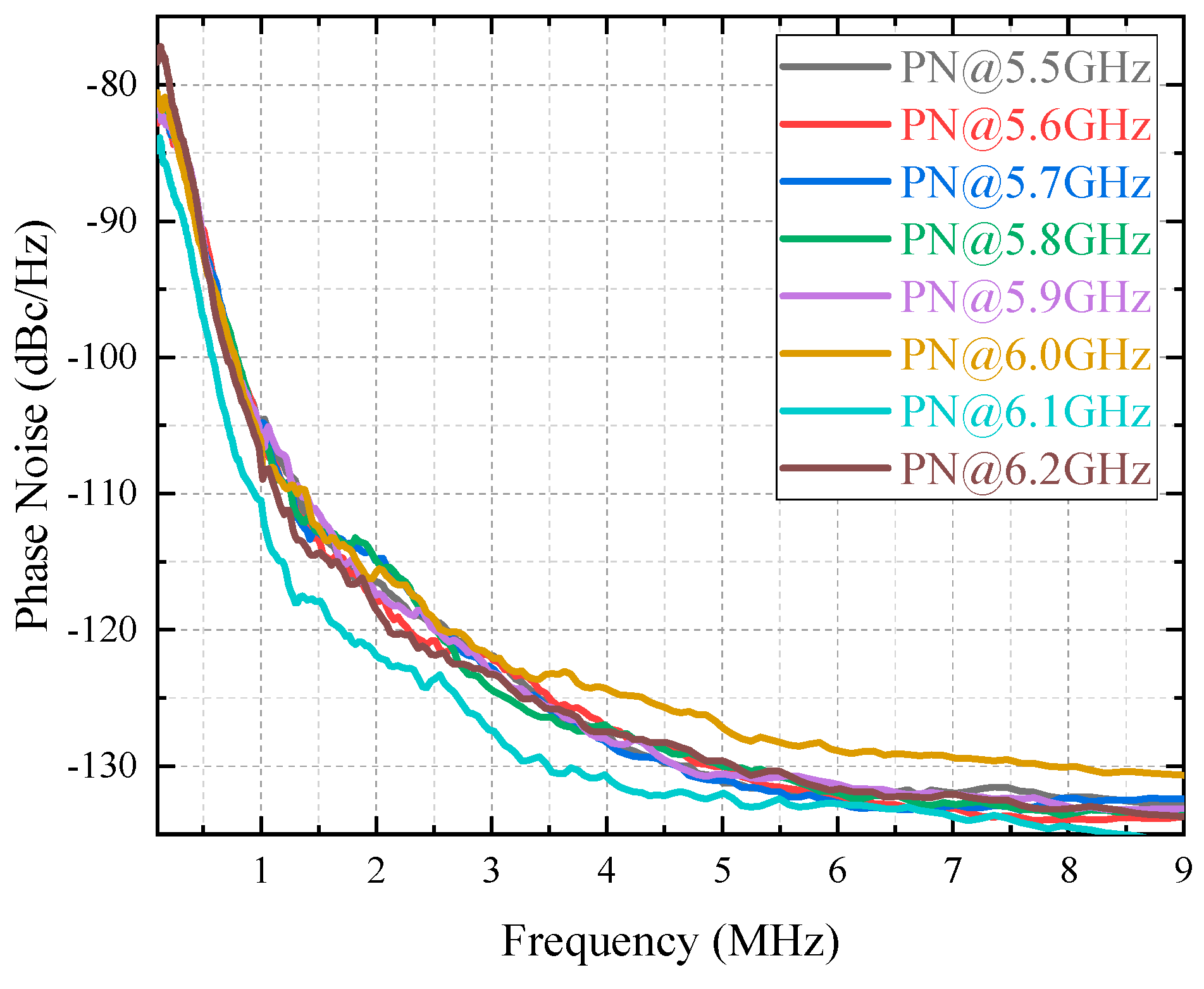
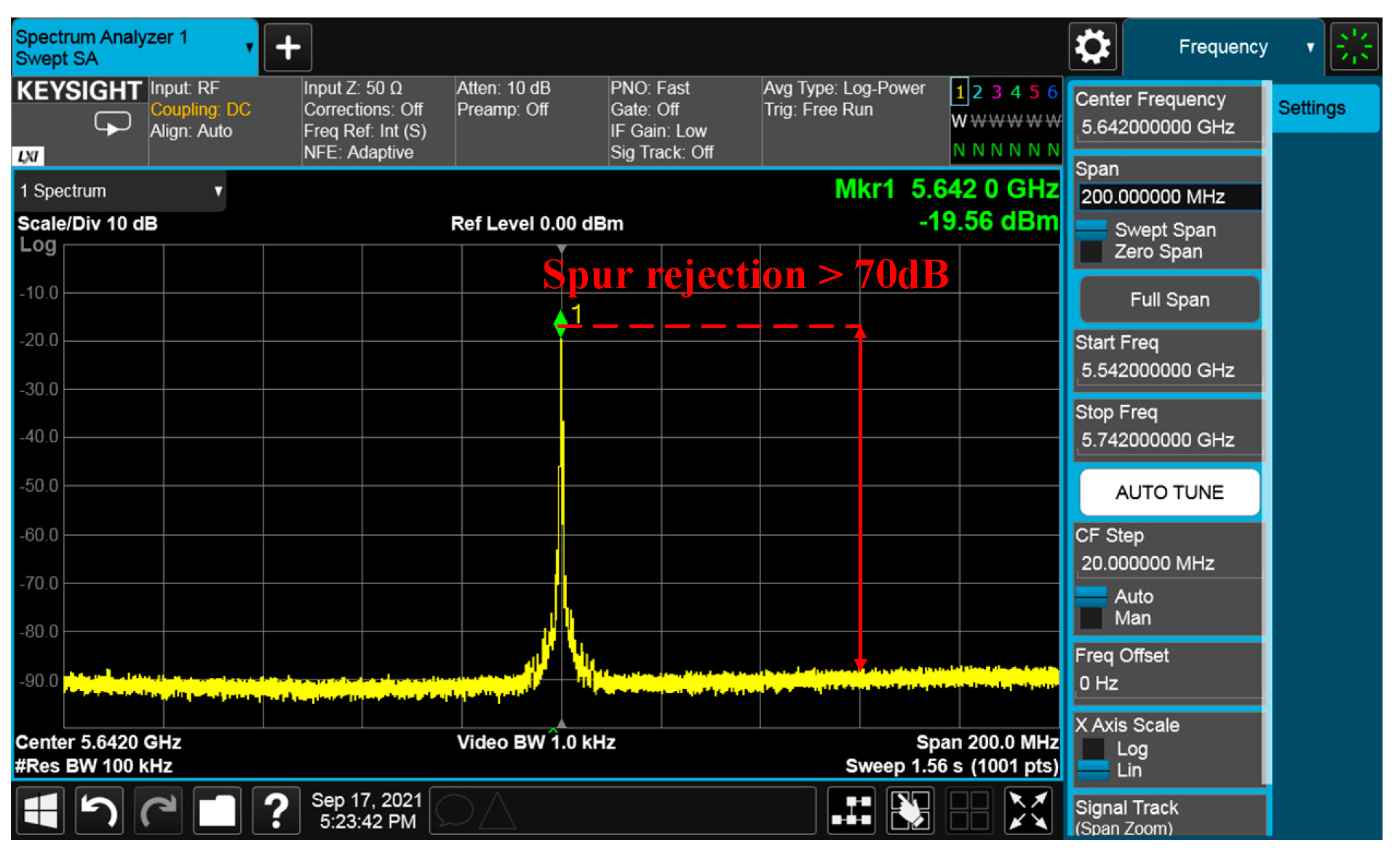
3. Measurement Results
4. Conclusions
Author Contributions
Funding
Institutional Review Board Statement
Informed Consent Statement
Data Availability Statement
Conflicts of Interest
References
- Li, C.C.; Yuan, M.S.; Liao, C.C.; Chang, C.H.; Lin, Y.T.; Tsai, T.H.; Huang, T.C.; Liao, H.Y.; Lu, C.T.; Kuo, H.Y.; et al. A Compact Transformer-Based Fractional-N ADPLL in 10-nm FinFET CMOS. IEEE Trans. Circuits Syst. I Regul. Pap. 2021, 68, 1881–1891. [Google Scholar] [CrossRef]
- Lee, D.G.; Nikoofard, A.; Mercier, P.P. A −254.1-dB FoM 2.4-GHz Subsampling PLL with a −76-dBc Reference Spur by Employing a Varactor-Based Cancellation Technique. IEEE Solid State Circuits Lett. 2020, 3, 102–105. [Google Scholar] [CrossRef]
- Chiu, W.-H.; Huang, Y.-H.; Lin, T.-H. A Dynamic Phase Error Compensation Technique for Fast-Locking Phase-Locked Loops. IEEE J. Solid State Circuits 2010, 45, 1137–1149. [Google Scholar] [CrossRef]
- Chen, Y.-W.; Yu, Y.-H.; Chen, Y.-J.E. A 0.18-mm CMOS Dual-Band Frequency Synthesizer with Spur Reduction Calibration. IEEE Microw. Wirel. Compon. Lett. 2013, 23, 551–553. [Google Scholar] [CrossRef]
- Bruss, S.P.; Spencer, R.R. A 5-GHz CMOS Type-II PLL with Low KVCO and Extended Fine-Tuning Range. IEEE Trans. Microw. Theory Techn. 2009, 57, 1978–1988. [Google Scholar] [CrossRef]
- Kuo, Y.-F.; Yang, M.-H.; Chiang, Y.-C. A 5-GHz Adjustable Loop Bandwidth Frequency Synthesizer with an On-Chip Loop Filter Array. IEEE Microw. Wirel. Compon. Lett. 2021, 31, 72–75. [Google Scholar] [CrossRef]


| Ref. | [3] JSSC 2010 | [4] MWCL 2013 | [5] TMTT 2009 | [6] MWCL 2021 | This Work |
|---|---|---|---|---|---|
| Process | 180-nm CMOS | 130-nm CMOS | 90-nm CMOS | 65-nm CMOS | 40-nm CMOS |
| Architect | CP array | CP array | Dual-path | LF array | Programmable PFD+CP array+ LF switch |
| Freq. (GHz) | 5.27~5.6 | 5.18~5.32 5.74~5.82 | 3.8~5.15 | 5.26~5.98 | 5.42~6.28 |
| Ref. (MHz) | 10 | 20 | <−70 | 10 | 120 |
| Loop BW (KHz) | 40 | 280 | 30 | 500 /1000 | 100 |
| Ref. Spurs (dBc) | <−70 | <−63 | <−70 | <−59 | <−70 |
| PN@1MHz(dBc/Hz) | −114 | −102 | −115 | −95~−102 | −107.2~−110.4 |
| Chip Size (mm2) | 1.61 | 0.76 | 1.5 | 1 | 0.83 |
| Pdc (mW) | 19.8 | 28.8 | 11 | 21.24 | 3.6/9.6 * |
| FoM (dBc/Hz) | −175.73 | −161.81~−162.64 | −177.61 | −163.73~−170.73 | −176.98~−180.18 −181.24~−184.44 * |
| FoMT (dBc/Hz) | −171.39 | −150.33~ −151.16 | −187.19 | −165.89~−172.89 | −180.32~−183.52 −184.58~−187.78 |
Publisher’s Note: MDPI stays neutral with regard to jurisdictional claims in published maps and institutional affiliations. |
© 2022 by the authors. Licensee MDPI, Basel, Switzerland. This article is an open access article distributed under the terms and conditions of the Creative Commons Attribution (CC BY) license (https://creativecommons.org/licenses/by/4.0/).
Share and Cite
Kang, L.; Lv, J.; Cheng, X. A 5.42~6.28 GHz Type-II PLL with Dead-Zone Programmability and Charge Pump Mismatch Trimming. Electronics 2022, 11, 4153. https://doi.org/10.3390/electronics11244153
Kang L, Lv J, Cheng X. A 5.42~6.28 GHz Type-II PLL with Dead-Zone Programmability and Charge Pump Mismatch Trimming. Electronics. 2022; 11(24):4153. https://doi.org/10.3390/electronics11244153
Chicago/Turabian StyleKang, Li, Juncai Lv, and Xu Cheng. 2022. "A 5.42~6.28 GHz Type-II PLL with Dead-Zone Programmability and Charge Pump Mismatch Trimming" Electronics 11, no. 24: 4153. https://doi.org/10.3390/electronics11244153
APA StyleKang, L., Lv, J., & Cheng, X. (2022). A 5.42~6.28 GHz Type-II PLL with Dead-Zone Programmability and Charge Pump Mismatch Trimming. Electronics, 11(24), 4153. https://doi.org/10.3390/electronics11244153