Abstract
The paper presents an analysis of power losses in a three-phase T-type neutral point clamped converter with insulated gate bipolar transistors. The paper’s main aim is to perform a detailed analysis of power losses in the converter operating as an active power filter. The study is based on the use of characteristics of semiconductor devices provided by the manufacturer in the module datasheet. Thanks to the analysis, it is possible to recognise the value of power losses, which facilitates the design of the converter cooling system. Identifying how power losses are distributed between the module switching devices is also possible. Power losses are shown as functions of the output current and module temperature. The analysis results were successfully verified by measuring power losses using a laboratory model of the converter with rated currents of 10 and 20 A. The obtained results indicate relatively low power losses and a relatively even distribution of power losses between the semiconductor devices. This is a superior feature of the three-level T-type neutral point clamped converter topology.
1. Introduction
1.1. Motivations
Power losses in power electronic converters play a crucial role in the design of their cooling system. Better recognition of power losses allows the converter designers to choose the appropriate cooling system in terms of its performance and size. This paper presents a detailed analysis of the power losses of the T-type Neutral Point Clamped (TNPC) converter, which is applied to the active power filter. The selection of this converter topology is dictated by the relatively low power losses and the fact that in this topology, as in other three-level topologies, the middle point of the dc circuit is available. In the case of an active filter, the neutral wire is connected to this middle point so that a fourth converter leg is not required. An additional advantage of the selected converter, in relation to the classical two-level topology, is the possibility of reducing the dimensions and the cost of the grid-side passive filter.
1.2. Literature Review
The topologies of multilevel converters were developed more than twenty years ago [1,2]. Multilevel converters were introduced mainly because of their possible use in converting medium voltage energy. Thanks to these converters, it was possible to efficiently convert electrical energy without using expensive and large transformers [3,4]. Over the years, it has become clear that many multilevel converter topologies often have better performance parameters than the classic two-level converter, even at low voltage levels [5,6,7,8,9]. One of the most important features of these converters is high efficiency, which was not always an obvious fact with the greater number of semiconductor devices used in converters with a very high number of voltage levels [10,11,12]. The high efficiency of the converter is an essential parameter because due to low power losses, the converter’s lifetime is longer, and the total cost of its operation is lower [13].
Because power loss evaluation of converters is a complex and multivariable issue [14,15,16,17,18,19], it is crucial to identify power losses in converters operating under various conditions accurately. The knowledge about converter power losses is vital for designers of converter cooling systems and manufacturers of semiconductor modules. Nowadays, semiconductor modules can be optimised for one converter operating mode but will not be suitable for other operating conditions. For example, the module optimised for grid-tied PWM rectifiers has diodes with higher current ratings than the module optimised for the PWM inverter. Typically, power loss analysis is performed individually for each converter topology.
This paper analyses the three-phase T-type neutral point clamped (TNPC) converter. The converter belongs to the group of three-level converters [20] in which there are also classical neutral point clamped (NPC) converter [21], active neutral point clamped (ANPC) converter [22], and advanced neutral point clamped converter [23].
The NPC converter, apart from lower power losses and better output voltage waveform, is characterised by an uneven distribution of power losses among semiconductor devices [24]. The solution to this issue is the development of the ANPC converter, which, using transistors instead of clamping diodes, makes it possible to distribute power losses between the semiconductor devices better. A further improvement of the three-level converter is the TNPC converter [25]. The power losses of this converter are analysed in this article. A very advantageous feature of this converter is the lower number of semiconductor switches compared to the ANPC or NPC topologies and lower power losses [26].
The selection of the T-type neutral point clamped converter for the active power filter is made mainly based on the requirements for reducing the size of the grid filter and the dimensions of the cooling system. The second aspect, which directly relates to the power loss analysis, is a topic of this paper. The other reason for the selection of the 3-level topology is the access to the medium point of the dc-link circuit. By the connection of the neutral wire to the medium point, it is possible to reduce the number of necessary converter legs, which additionally reduces the converter losses.
The proposed method of calculating power losses in the TNPC converter is similar to the method proposed in [26]. The difference is that in [26,27,28], the semiconductor switch output characteristics have been approximated by linear functions. Still, in this paper, the approximation is made with more precise power functions that also recognise the influence of temperature on these characteristics. Further, the functions of energy losses are more accurately presented than in [26,27,28]. The results of power loss analysis are shown in this paper mainly as a function of the output current and temperature with the switching frequency and phase-shift angle set to constant values.
Currently, intensive works are ongoing worldwide on converters with SiC MOSFETs, such as the TNPC converter [29] or the ANPC hybrid converter combining the IGBTs with the SiC-MOSFETs in a single topology [30]. This topology is characterised by even lower power losses than the TNPC topology. Despite the increasing share of converters with SiC-MOSFET transistors, the topology of the TNPC converter using IGBT transistors still has good properties. Such properties include low power losses, favourable output voltage, and a low level of generated disturbances. It is believed that accurate recognition of the power loss is needed.
1.3. Contribution
The analysis presented in this paper is performed for the TNPC converter operating as an active filter. The details on the laboratory model of the TNPC converter are given in [31]. This converter practically generates reactive current with only a small share of power losses constituting the active power. Connecting the converter to the electrical grid causes the modulation index and the phase-shift angle to be almost constant. This, in turn, means that the analysis presented in the article can be performed with a limited number of changing parameters affecting power losses.
Power losses generated in the TNPC converter should be small due to the long operation time of the converter and the need for its long lifetime. In many cases, the lifetime of power electronic converters is approx. 20 years, during which even minor losses contribute to high costs for the end-user of the converter.
Many works on power losses in the TNPC converters are devoted to inverters with a phase-shift angle close to zero. For this mode of operation, the natural parameter is the converter efficiency, which, in the case of the converter operating as an active filter, cannot be used. The converter efficiency parameter is replaced in this paper by a per kVA power loss ratio. Such a parameter can be useful when comparing different converter topologies or different active filter solutions.
The main contributions of this paper are listed below.
- The development of a detailed analysis of power losses for the TNPC converter. This analysis allows the user to quickly determine the power losses when one or more operating parameters of the converter or its design parameters are changed. The developed power loss model of the TNPC converter is an analytical model that has an advantage over the simulation model because obtaining results in the form of characteristics is much faster. However, this is done at the expense of the use of a number of mathematical equations, which in the case of simulation models do not need to be used.
- The model uses an accurate approximation of characteristics of semiconductor devices for currents changed between 0 and the rated current value. This approximation guarantees that power losses are better mapped than in the case of using a model with a piecewise-linear approximation.
- The analysis proposed in the paper is based on characteristics obtained from the semiconductor datasheet. The development of such an analysis is faster when compared to analyses requiring the prior measurements in specific test circuits as is typically used in the literature, e.g., [27,28]. Using the datasheet characteristics can be done, however, when the parameters of the converter gate circuit and the dc-link circuit are comparable to the parameters used in the datasheet.
- The analysis proposed in the paper has regard to eight different parameters influencing the power losses they are (1) output current amplitude of the fundamental component, (2) dc-link voltage, (3) switching frequency, (4) phase-shift angle of the fundamental components of output current and voltage, (5) semiconductor temperature, (6) modulation index, (7) PWM modulation technique, and (8) gate resistances in a transistor driver circuit. Such analysis is comprehensive and can be applied to converters operating under different conditions. In this paper, the operational conditions are restricted to the operation of the active power filter.
It is believed that a detailed power loss analysis for the TNPC converter is needed and is an original contribution. In many papers, power losses are presented only for a specific case of converter operation, and this is mainly for the inverter operation. In this paper, power losses are shown more broadly.
1.4. Paper Organisation
This paper is organised as follows. Section 2 shows the complete power loss analysis in the TNPC converter. Section 3 presents the experimental validation of power loss analysis on the example of two test setups with TNPC converters. Section 4 presents the conclusions. After the conclusions, the nomenclature is presented in which all parameters used in this paper are listed. After that, Appendix A lists all values of the design parameters of the TNPC converter in the study.
2. Power Loss Analysis
Most converter power losses in power electronic converters are generated due to the conduction and switching of semiconductor devices. This paper only considers these two sources of losses generated in a T-type NPC converter without considering the dead-time effect and dc-link voltage ripple. Both conduction and switching losses are calculated analytically based on approximated IGBT module characteristics provided by the manufacturer [32]. Although a single leg of the TNPC converter consists of four transistors and two diodes, as seen in Figure 1, power losses in only three semiconductor devices are considered. They are transistors T1 and T2 and diode D4. This approach is adopted because transistors T1 and T4 have the same parameters and are exposed to the same currents and voltages phase-shifted by half of the fundamental period. A similar situation exists for transistors T2 and T3 and diodes D1 and D4. Other losses generated in the converter are also considered, among which are the dc-link capacitor losses and losses generated in pcb tracks due to resistance.
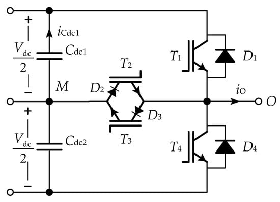
Figure 1.
Single leg of the TNPC converter consisting of two conventional IGBTs, T1 and T4, two reverse blocking RB-IGBTs, T2 and T3, and two diodes, D1 and D4.
2.1. Conduction Power Losses
The conduction losses (Equation (1)) are calculated separately for each switching device by calculating the average value of the power obtained from the integral of instantaneous power pX (t) = iX (t) vX (t), where iX (t) is the device X current and vX (t) is the voltage across this device. The integration of instantaneous power is performed in the ωt domain from angle α1 to α2. Because the device current iX (ωt) is a modulated phase current iO (ωt), it must be multiplied by the modulation function SX (t), iX (ωt) = iO (ωt) SX (ωt). The modulation function is closely related to the modulating signal SM (ωt) used in the converter PWM modulator.
2.1.1. Output Characteristic Approximation
In the presented power loss analysis, the output current is assumed as sinusoidal, iO = Im sin (ωt − φ), and the device voltage vX (t, TX) is a function of the current and device junction temperature TX as in Equation (2).
where VX0 (TX) is a temperature-varying threshold voltage, VXn (TX) is a temperature-varying device voltage at nominal current In, and 1/nX (TX) is a temperature-varying exponent of the power function representation of the device on-state characteristic. The threshold voltage VX0 (TX) and nominal voltage VXn (TX) are linear functions obtained from on-state characteristics at temperatures TX = 25 and TX = 125 °C (Equations (3) and (4)).
The values of function parameters given in Equations (3) and (4) for the analysed IGBT TNPC module are listed in Table 1 and shown in Figure 2.

Table 1.
Parameters of temperature-varying functions VX0 (TX) and nominal voltage VXn (TX) of transistors T1 and T2 and diode D4.
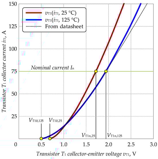
Figure 2.
Output characteristic of transistor T1 from the three-phase TNPC IGBT module 12MBI75VN120−50 (VCES = 1200 V, In = 75 A).
Finding exponent nX(TX) of the power function is performed by applying the curve fitting method to a normalised function (Equation (5)), which is obtained from Equation (2)
where vX (iX, TX) is the output characteristic voltage taken from the IGBT module datasheet. For transistor T1, the normalised function (Equation (5)) for TT1 = 125 °C is depicted in Figure 3. The normalised function (Equation (5)) always crosses points (0, 0) and (1, 1) even though the temperature TX varies.
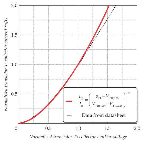
Figure 3.
Normalised output characteristic of transistor T1 from the TNPC module 12MBI75VN120-50 (VCES = 1200 V, In = 75 A) for temperature TT1 = 125 °C.
In Figure 3, one can see that the normalised function iT1/In for TT1 = 125 °C with nT1 (125 °C) = 1.65 matches the data for a normalised voltage in the range between 0 and 1. Still, for voltages between 1 and 2, some discrepancy is observed. This discrepancy is not problematic because it occurs for currents higher than the rated value In in the range, which is out of the scope of the analysis presented in this paper. The best-fitting exponents for normalised functions of all converter devices are collected in Table 2; these parameters are given for temperatures TX = 25 and TX = 125 °C.
Table 2.
Exponents of power functions for output characteristics of all TNPC converter devices T1 and T2 and D4 for two temperatures TX = 25 and TX = 125 °C.
The exponent nX (TX) given in Equation (5) is a function of temperature TX and is approximated by a linear function obtained from two points, nX (25 °C) and nX (125 °C), which are calculated from Equation (6).
After substituting Equations (2)–(6) into Equation (1), each device’s conduction losses are given as Equation (7).
2.1.2. Conduction Angles and Modulation Function
Power loss analysis is performed in the ωt domain. Therefore, it is essential to identify the corresponding conduction angles for each semiconductor device in the TNPC converter (Figure 1). All devices’ currents for exemplary output current and modulation index ma are shown in Figure 4.
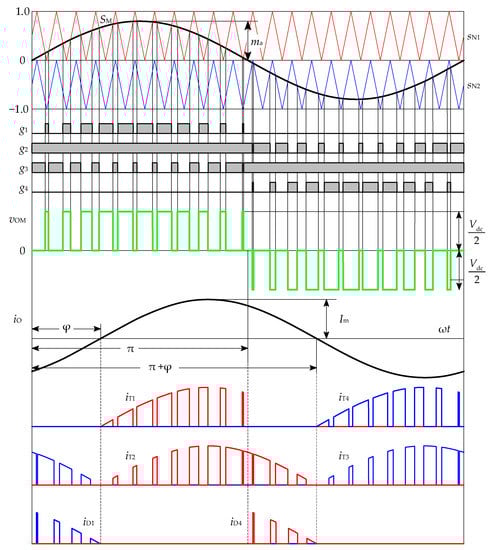
Figure 4.
Output voltage vOM and all device currents of TNPC single-leg for modulation index ma = 0.8. (The switching frequency is intentionally reduced to improve the readability of the waveforms).
Each TNPC converter device conducts switched currents for different angles. The angle at which a device starts conducting is referred to as α1, and the angle when a device stops conducting the current is α2. Both angles are different for each converter device, as is seen in Figure 4 and Table 3. In Figure 4, device currents are modulated according to modulation functions SX (ωt). For example, transistor T1’s current, iT1, is modulated by function ST1 (ωt) = SM (ωt), but transistor T2’s current is modulated by the complementary function ST2 (ωt) = 1−SM (ωt) for ωt = (0, π) and ST2 (ωt) = 1 + SM (ωt) for ωt = (π, 2π). Modulation functions of all device currents are given in Table 3.
Table 3.
Conduction angles α1 and α2 and modulated functions SX (ωt) of devices T1, T2 and D1.
2.1.3. Results of Conduction Power Losses
After substituting all parameters related to device output characteristics, conduction angles and modulation function into Equation (7), the total conduction power losses can be calculated. It is assumed that the output current is sinusoidal with the phase-shift-angle equal to φ = π/2 and the modulation index ma = 0.86. The phase-shift angle φ = π/2 corresponds to the converter operation as a reactive power compensator. In practice, the converter operates with a small share of power losses, which reduces the phase-shift angle to nearly φ = 89°. Since such a difference in the angles does not significantly impact the value of the power losses, the value of φ = π/2 is assumed. The analysis also assumes that power losses are calculated for the same junction temperature of all switching devices. The conduction losses of the three-phase TNPC converter given as a function of temperature Tj are depicted in Figure 5a. These losses are calculated as the sum of losses in all devices multiplied by the number of phases and duplicated due to the number of devices in each converter leg, Pcon = 6PconT1 + 6PconT2 + 6PconD4.
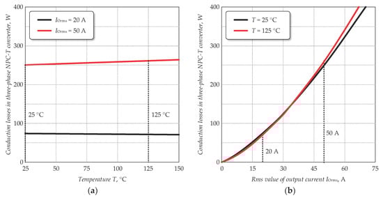
Figure 5.
Conduction power losses of the three-phase TNPC converter for the modulation index ma = 0.86 and the phase-shift angle φ = π/2 given as (a) a function of temperature for the output current rms value IOrms = 20 and 50 A and (b) a function of the rms value of the output current for temperatures of 25 and 125 °C.
From the characteristics shown in Figure 5b, conduction power losses for the current of IOrms = 20 A decrease with temperature increase. Such behaviour of power losses can be explained by the negative thermal coefficient occurring in output device characteristics present for currents below 15 A for transistors T1 and T4 (as in Figure 2), below 35 A for transistors T2 and T3, and below 30 A for diodes D1 and D4.
Conduction power losses for the device temperature of 25 °C and the output currents of IOrms = 20 and 50 A equal 73.6 and 250.1 W, respectively. The distribution of conduction power losses among converter devices is not even, as presented in Figure 6.
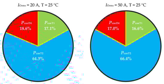
Figure 6.
Distribution of conduction power losses among TNPC converter devices for modulation index ma = 0.86 and the phase-shift angle φ = π/2, temperature T = 25 °C and two rms values of the output current 20 and 50 A.
From Figure 6, one can see that the distribution of conduction power losses for a constant phase-shift angle φ and modulation index ma is slightly different with the change of the output current rms value. The RB-IGBT transistors T2 and T3 have the largest share of conduction losses. This is because these transistors conduct modulated currents for half of the fundamental period (α2 − α1 = π) compared to transistors T1 and T4, which conduct modulated currents for α2 − α1 = π − φ = π/2 (for φ = π/2) and diodes D1 and D4, which conduct such currents for α2 − α1 = π + φ − π = π/2.
2.2. Switching Power Losses
The TNPC converter has smaller switching power losses compared to other converters. This is because switching losses in transistors T1 and T4 occur at blocking voltages Vdc/2 even these transistors must withstand the entire Vdc similarly as in a two-level converter. In a two-level converter, power losses occur at voltages Vdc; thus, switching losses, which are proportional to the blocking voltage, in the TNPC converter is reduced to half of such losses of a two-level converter. This is true when a TNPC converter uses identical transistors as a two-level converter. However, RB-IGBTs (T2 and T3) have better switching performance because they are designed for withstanding the voltage of Vdc/2.
Switching power losses are generated in IGBTs during transistor turn-on and turn-off processes. They can be calculated as an average value of a sum of energies during turn-on Eon and during turn-off Eoff over the fundamental period multiplied by the switching frequency fS. These energies are functions of the device current iX (ωt), device temperature TX, blocking voltage Vb and the resistances of the gate circuit RG. In the presented analysis, resistances RG are chosen to the same values selected by the manufacturer in the module datasheet [32]. However, due to the resistance of driver output, the resistances are equal RG1 = 3.2 Ω, RG2 = 5.7 Ω. The switching power losses are an integral of energies in the interval restricted by switching angles α3 and α4 (Equation (8)).
where Err is the switching energy generated in the diode due to reverse recovery. For diodes, energies Eon and Eoff are equal to zero; similarly, for transistors, Err is equal to zero.
2.2.1. Switching Angles
The switching angles α3 and α4, which are not the same as conduction angles, can be shown by device current and voltage waveforms in Figure 7 and are listed in Table 4.
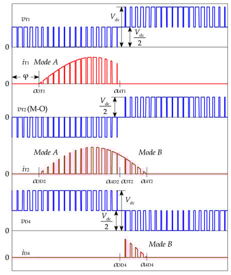
Figure 7.
Current and voltage waveforms of devices T1, T2, D2 and D4 with marked switching angles α3 and α4.
Table 4.
Switching angles α3 and α4 of devices T1, T2, D2 and D4 with indicated switching mode.
Contrary to conduction losses, the switching losses in transistor T2 and diode D2 are calculated separately. The RB-IGBT conduction losses are taken together for transistor T2 and diode D2, which are connected in series and are represented by a single output characteristic. The switching losses in RB-IGBT are separated for transistor T2 and diode D2. For , transistor T2 is still turned on; thus, for positive device currents, which is for , the switching power losses occur on diode D2 due to its reverse recovery Err. This phenomenon can be explained by the fact that in this angle range, the voltage vT2 is switched between negative voltage −Vdc/2 and 0. For iT2 > 0 and , switching losses are generated in transistor T2. In Table 4, one can see the modes of commutation (Mode A and Mode B), which correspond to modes distinguished by the manufacturer of the IGBT module. For Mode A, losses are generated in transistors T1 and T4, but because the switching losses in T4 are the same as in T1, only losses in T1 are calculated. In mode A, switching energies Err are generated in diodes D2 and D3. In mode B, switching energies are generated in transistors T2 (and T3) and diodes D4 and D1.
2.2.2. Characteristics of Switching Energies
All characteristics of switching energies Eon, Eoff and Err are presented in Figure 8 as functions of the device current for both switching modes. These functions are given for two temperatures TX = 25 and TX = 125 °C, the blocking voltage Vdcref = 300 V, the gate resistors RG1 = RG4 = 2.2 Ω and RG2 = RG3 = 4.7 Ω and for the gate voltages ranging from −15 to +15 V.
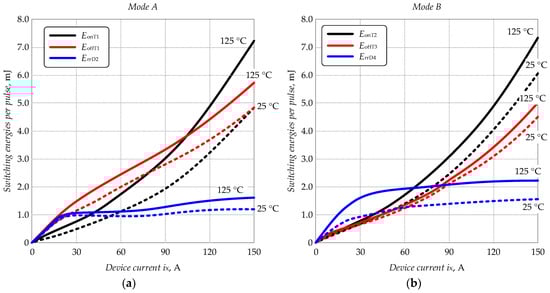
Figure 8.
Switching energies given as a function of device current for module 12MBI75VN120-50, (a) in mode A, energies Eon and Eoff occur in transistors T1 and T4, reverse recovery energy Err occur in diodes D2 and D3, (b) in mode B, energies Eon and Eoff occur in transistors T2 and T3, reverse recovery energy Err occur in diodes D1 and D4.
Switching energy characteristics for transistors given in Figure 8 can be approximated by quadratic functions as in Equation (9) and multiplied by a factor kRGXY representing the effect of the gate resistance on switching losses. The approximating function coefficients for device current from 0 to 75 A are listed in Table 5.
Table 5.
Coefficients of approximating quadratic functions of transistor switching energies as in Equation (9).
The approximation of diode reverse recovery energy characteristics by quadratic functions does not provide satisfactory results; therefore, the cubic function (Equation (10)) is chosen for these characteristics. The coefficients aYX, bYX, cYX and dYX are obtained using a fitting algorithm for device currents from 0 to 75 A.
The approximating cubic function coefficients for reverse recovery energy losses in diodes are listed in Table 6.
Table 6.
Coefficients of approximating cubic functions of diode reverse recovery energies.
The temperature influence on switching energies in each device is considered by approximation of each polynomial coefficient z = a, b, c and d by linear function obtained from two points zYX,25 (for TX = 25 °C) and zYX,125 (for TX = 125 °C), which is given in Equation (11).
2.2.3. Results of Switching Power Losses
The calculation of switching power losses in all four semiconductor devices is performed using Equations (12)–(15). In the analysis, it is assumed that the junction temperature of all switching devices is the same, the switching frequency is fS = 20 kHz, and the blocking voltage Vb is equal to Vdc/2 = 370 V (while the blocking voltage for which datasheet data is obtained is equal to Vdcref = 300 V). Total switching power losses in the three-phase TNPC converter is the sum of switching losses of all devices multiplied by six as in Equation (16).
The characteristic of switching power losses Equation (16), as a function of device temperature (with the assumption that all devices are exposed to the same temperature), is shown in Figure 9a. As presented, the switching losses increase with the temperature increase and are between 1.6 and 2.3 times higher than the conduction losses for IOrms = 20 A and constitute 0.9 to 1.2 of conduction losses for IOrms = 50 A. Unlike conduction power losses, switching losses (Equation (16)) always have a positive thermal coefficient, as shown in Figure 9b. The switching power losses are nearly linear functions of current compared to quadratic functions for conduction losses.
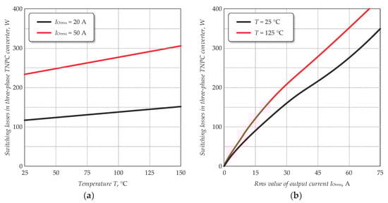
Figure 9.
Switching power losses Psw of three-phase TNPC converter for the switching frequency fS = 20 kHz, half of dc-link voltage Vdc/2 = 370 V and the phase-shift angle φ = π/2 given as (a) a function of temperature for the output current rms value IOrms = 20 and 50 A and (b) a function of the rms value of the output current for temperatures of 25 and 125 °C.
It is interesting that for small currents, switching losses converge to zero. This is because the output current is assumed as sinusoidal in the presented analysis. In the real converter, current ripples are present in the output current, increasing the switching losses particularly close to zero current fundamental components. This phenomenon is presented in the next section.
The distribution of switching losses among devices (Equations (12)–(15)) is presented in Figure 10 for the rms value of the output current IOrms = 20 and IOrms = 50 A. This distribution shows that the highest power losses occur in transistors T1 and T4, opposite to the conduction losses where the highest losses occur in transistors T2 and T3.
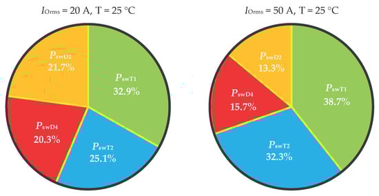
Figure 10.
Distribution of switching power losses among TNPC converter devices for phase-shift angle φ = π/2 and rms value of the output current equal to 20 and 50 A.
2.3. DC-Link Capacitor Losses
In addition to power losses in semiconductor devices, this paper also attempts to estimate the losses in both dc-link circuit capacitors Cdc1 and Cdc2, as in Figure 1. Capacitor power losses PCdc are generated in two capacitors due to non-zero values of equivalent series resistance RESR and are calculated from Equation (17).
where Idcrms is the rms value of the capacitor current idc. The waveform of the capacitor current idc1 is shown in Figure 11.
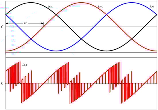
Figure 11.
Output currents iOA, iOB and iOC waveforms together with the capacitor current iCdc1 (The switching frequency is intentionally reduced to improve the readability of the capacitor current waveform).
The rms value of the capacitor current depends on phase-shift angle φ, modulation index ma, the switching frequency f, and output current rms value IOrms. Because the first three listed parameters are set as constant in the paper, it is possible to present the capacitor current rms value only as a function of the output current rms value. The simulation model performed in GeckoCIRCUITS shows that the capacitor current rms value equals 9.75 A when the output current is IOrms = 20 A. Because the rms value of the capacitor current depends linearly on the output current, the ratio of these currents is always constant and equals kICdc = 9.75 A/20 A = 0.488.
In the analysed converter, the equivalent series resistance of capacitor batteries, measured for a frequency of 20 kHz, is equal to RESR = 35 mΩ; thus, total capacitor power losses can be calculated from Equation (17) and given as a function of the output current, as is shown in Figure 12.
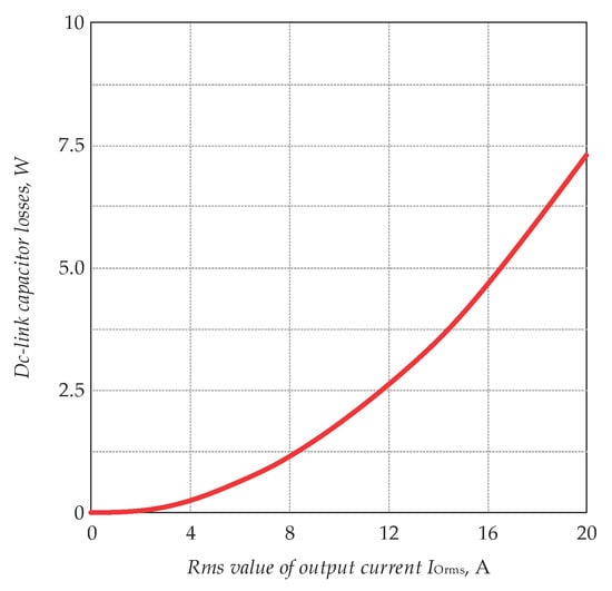
Figure 12.
Dc-link capacitor power losses as a function of the rms value of the output current.
It is evident from Figure 12 that the power losses in capacitors account for less than 10% of the conduction losses or switching losses generated in semiconductor devices, and these losses should not be ignored in the power loss analysis of the TNPC converter.
2.4. Total Power Losses
The sum of conduction and switching power losses together with capacitor losses are referred to as total power losses. Because the analysed converter operates as a grid-side converter, the modulation index ma is nearly constant and equal to ma = 0.86, and its influence on power losses is out of the scope of this paper. The switching frequency, a major parameter significantly impacting switching losses, is also set to fS = 20 kHz. Dc-link voltage is Vdc = 740 V, satisfying the requirement for maVdc/2 = Um, where Um is the magnitude of the phase voltage. The capacitor power losses are present for a set temperature of 25 °C because it is assumed that capacitors are located at a relatively large distance from the IGBT module, which is a significant heat source inside the converter. Total power losses as a function of temperature and current are shown in Figure 13.
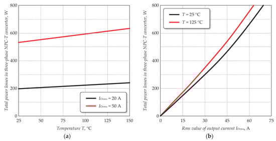
Figure 13.
Total power losses in the three-phase TNPC converter are given as (a) a function of temperature T and (b) a function of the rms value of the output phase current IOrms.
The distribution of the sum of power losses (Pcon + Psw + PCdc) generated in converter components is presented in Figure 14.
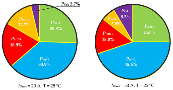
Figure 14.
Distribution of power losses generated in TNPC converter devices the output current equal to 20 and 50 A.
2.5. Per kVA Power Loss Ratio
For a converter operating with a large share of reactive power, such as the active power filter, the classical definition of converter efficiency cannot be applied. This is because the converter is connected to one power port, and there are no input and output powers as other converters transfer active power between power ports. In this paper, power losses are referenced to the apparent power as Equation (18), where S1 is the apparent power for fundamental frequency fm, and Vll is the line-to-line voltage rms value.
The definition of the power loss ratio is similar to the one used for capacitors used for reactive power compensation. These losses are a function of the output current rms value and are shown in Figure 15. The value of the current equal to 75 A corresponds to the apparent power of 52 kVA.
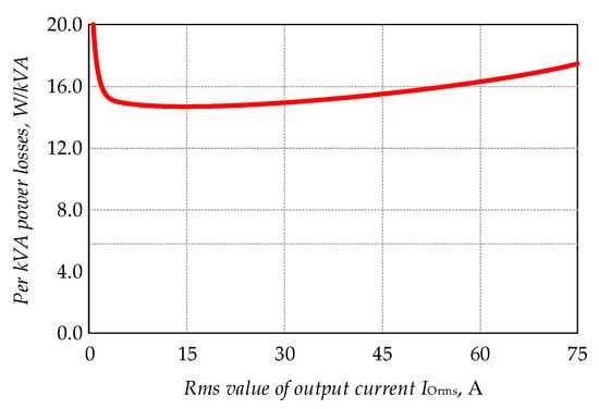
Figure 15.
Per kVA power losses of the TNPC converter are given as a function of the output current.
3. Experimental Validation of Power Loss Analysis
The laboratory model of a three-phase TNPC converter has been tested to validate the presented power loss analysis. This laboratory model is a part of a four-wire active power filter with the neutral wire connected to the medium point of the dc-link capacitors [31]. The converter is based on a three-phase TNPC IGBT module 12MBI75VN120-50, the parameters of which are used in the analysis shown in Section 2. For the validation of the power loss analysis, the following two experimental tests have been carried out:
- Test of the TNPC converter supplied from dc power supply operating with a three-phase inductor at the converter output;
- Test of the grid-connected TNPC converter;
Both tests are performed with a nearly constant modulation index ma = 0.86 with a significant reactive component of the output current.
3.1. Power Losses of TNPC Converter Supplied from the DC Power Supply
The converter is supplied from two dc power supplies, each supplying variable voltage Vdc/2. A three-phase inductor with a nominal inductance of LAC = 33 mH is chosen as a load. The sum of the inductor resistance and the resistance of wires equals RLAC = 0.49 Ω leading to the phase-shift angle φ = 87.6°. Such a load has been chosen to carry out experimental tests at Vdc/2 = 370 V with modulation index ma = 0.86, at which the output current rms value equals a rated value IOrms = IOn = 20 A. The selected value of Vdc/2 equals the rated value of the tested active power filter. The switching frequency is 20 kHz. The tests have been carried out with a WT5000 power analyser connected to the converter, as shown in Figure 16. The photograph of the experimental setup is presented in Figure 17.
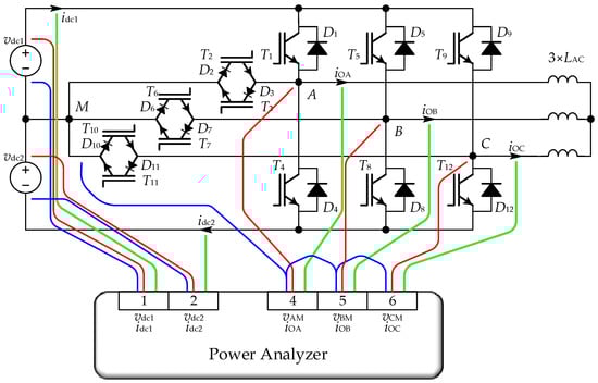
Figure 16.
Schematic of the experimental setup for power loss measurement in the three-phase TNPC converter supplied from dc power supplies and with three-phase inductors LAC at the converter output.
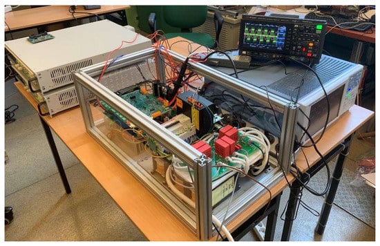
Figure 17.
Experimental setup for power loss measurement in the three-phase TNPC converter.
The results of power loss measurements are collected in Table 7. During the test, five input elements were used, two for the dc-side of the converter and three for the ac-side. Power is measured at the input as Pin and the output as Pout, together with calculating the power losses as their difference. Figure 18 shows the exemplary screen images from the power analyser for the rms output current IOrms = 20 A.
Table 7.
Results of power loss measurement of TNPC converter operating with 33 mH inductors.
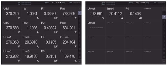
Figure 18.
Results for power loss measurement from the WT5000 power analyser.
In Table 7, the measurement data for the dc-side are represented by two voltages, vdc1 and vdc2, and currents idc1 and idc2. For the ac-side, due to the space limitation, only one current IOrms is given, which is the average value of the three-phase currents. The difference between these currents (Figure 18) results from using a three-phase three-limb coupled inductor in which the lowest current occurs in the phase where the winding is wound around the centre limb.
The measured power losses and theoretical total power losses, given for conditions during the test, are shown in Figure 19 as a function of the output current.
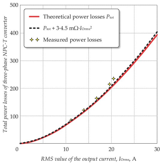
Figure 19.
Power losses in the three-phase TNPC converter supplying three-phase inductor LAC = 33 mH, operating with a varying dc-link voltage and constant modulation index ma = 0.86.
The theoretical losses are presented for an assumed temperature T = 45 °C, the varying blocking voltage, constant phase-shift angle φ = 87.6°, and modulation index ma = 0.86. The phase-shift angle is adopted from each phase active power measurement according to Equation (19). The reason for the temperature T selection was that a forced cooling system set this temperature as a steady-state thermal value.
where PA, PB and PC are phase A, B and C output powers and IOArms, IOBrms and IOCrms are corresponding rms values of phase currents. In Equation (19), it was assumed that in each phase, the inductance of the inductor is the same and equal to LAC = 33 mH.
From Figure 19, it is evident that the measured losses are higher than the theoretical ones. This is because, in the converter, additional power losses are generated in pcb wires and connectors. The resistance of all wires and connections has been measured and is estimated to be 4.5 mΩ for each converter phase. The characteristic of the theoretical total power losses with additional losses is also shown in Figure 19. The correlation between theoretical and measured losses is high. The presented measurements have been performed for varying dc-link voltage, which did not correspond to the normal operation of the converter. However, they reveal the correct dependence of losses on dc-link voltage.
3.2. Power Losses of Grid-Connected TNPC Converter
In this test, the TNPC converter has been connected to the three-phase 3 × 400 V grid and operated as the active power filter. The dc-link voltage was kept constant at Vdc/2 = 370 V. The converter was connected to the grid through the LCL filter with the sum of inductances Lf = Lf1 + Lf2 = 750 + 150 μH = 900 μH and filter capacitance Cf = 4.4 μF. During the measurement of power losses, the converter has been generating capacitive and inductive reactive power. These power losses are compared with theoretical power losses obtained by applying the method proposed in Section 2. For theoretical power losses, it is assumed that the phase-shift angle φ = 90.0° and the modulation index ma = 0.86 for all output current rms values IOrms ranging from =0 to 10 A. This assumption also neglects the small capacitive current of the filter capacitor. In the analysis, the switching frequency is considered equal to 20 kHz. The tests have been carried out with a power analyser connected to the converter, as shown in Figure 20.
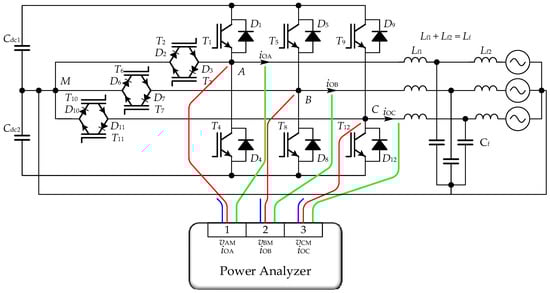
Figure 20.
Schematic of the experimental setup for power loss measurement in the three-phase TNPC converter connected to the grid and operating as an active power filter.
The results of the power loss measurements are listed in Table 8, where power losses for inductive output currents are given. The output voltage and current waveforms for inductive reactive power generation at IOrms = 11.0 A are shown in Figure 21. The measurement power losses of the three-phase TNPC converter are compared with the theoretical power losses as given in Section 2 and are shown in Figure 22. Apart from generating reactive power, the analysed converter also consumes active power in the form of power losses. Nevertheless, the analysis assumes that the phase-shift angle φ = 90°. The analysis does not consider the slight change in modulation index ma with the output current change. Thus, the modulation index is constant and equal to ma = 0.86. Due to a stable thermal condition guaranteed by the cooling system, the temperature during the test was constant and equal to T = 45 °C. This temperature was measured by an NTC resistor from the IGBT module.
Table 8.
Results of power loss measurement of the TNPC converter operating as the active power filter.
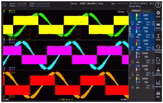
Figure 21.
Exemplary waveforms of the three-phase TNPC converter output voltages and currents for rms value of the output current IOrms = 11.0 A and inductive reactive power generation.
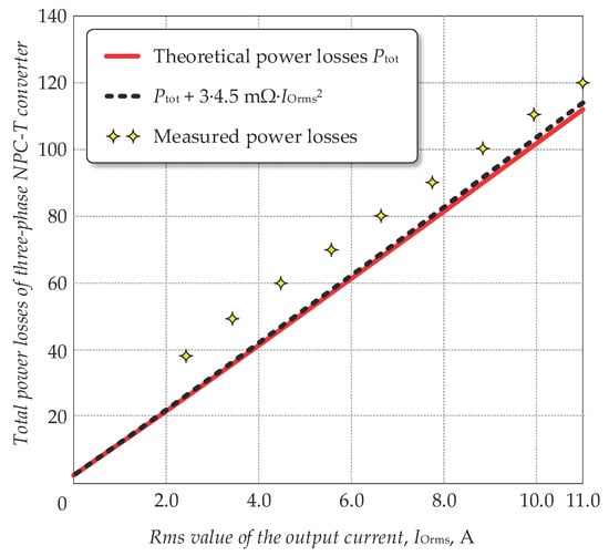
Figure 22.
Power losses in the three-phase TNPC converter generating a reactive current.
As seen in Figure 22, the measured power losses are always higher than the theoretical losses. This is particularly true for low rms values of the output current. The main reason for such a difference in power losses is the switching frequency output current ripples. It should be noted that during the first tests, when the converter was supplied from the dc power supply, such output current ripples did not occur due to relatively large inductances of the three-phase inductor, which were equal to LAC = 33 mH. Another reason for the discrepancy between measurement data and theoretical results is the assumption that the device temperature is the same as the temperature of the module base. In a real module, the device temperature is higher by several degrees Celsius.
It should be noted that similar power loss characteristics can be obtained for the generation of capacitive reactive power. In the case of using different design parameters of the active power filter, i.e., with the different switching frequency, dc-link voltage, and temperature, the proposed power loss analysis can also be applied.
4. Conclusions
This paper presents a detailed analysis of power losses of a three-level T-type NPC converter. The study is performed thoroughly; however, the focus is on the converter operation as an active power filter. The accurate recognition of power losses allows the converter designer to carry out the proper steps during the converter designing stages, which, among others, are: setting the switching frequency, designing the cooling system, and designing the gate drivers.
In the paper, the detailed power loss analysis is based on characteristics provided by the IGBT module manufacturer. Obtained power losses are given as functions of the rms value of the output current and temperature. However, they can be extended to other parameters influencing them. Power losses are divided into conduction and switching losses with a given distribution among all semiconductor devices of the T-NPC converter. This division of power losses is essential for designers of IGBT modules and converters because it is possible to find the semiconductor device with the highest power losses for different operating conditions. In the analysed converter operating as the active power filter, the most significant share of losses occurs in transistors T2 and T3. Together with losses in diodes D2, they constitute nearly half of the total power losses. These even shares of power losses are a very advantageous feature of the converter.
The measured power losses agree with the losses obtained from the analysis. In the first test, the converter output current has been changed from 10 to 20 A. The difference between the analytical results and measured power losses ranged from 5% to 9%. It is believed that such a good correlation between the measured and analysed results is due to the very small output current ripples in the test, which are neglected in the analysis.
In the second test of the TNPC converter operating as an active power filter, the power losses from the analysis were consistent with the measurements, but better results were obtained for operation at higher currents, close to 11 A. For lower currents, the compliance is lower. This is believed to be due to the presence of current ripples for lower currents power losses that are not the same as for sinusoidal currents.
The TNPC converter has been tested with the rms values of the current ranging from 0 to 20 A when it was supplied from the dc power supply and from 0 to 10 A when it was connected to the grid. For higher currents, the discrepancy between power losses observed during the experiments and theoretical ones can be explained by the existence of higher component junction temperatures than the single temperature measured on the module and the existence of output current ripples.
The future works on presented detailed power loss analysis can be extended with the thermal model of the IGBT module. In such an extended model, the temperatures of individual semiconductor devices are not the same and are higher than the temperature of the module base plate.
It should be noted that the detailed power loss analysis can also be applied to other converter topologies. In such a case, the modification of some parameters is required that relate to different conduction angles, switching angles and modulation functions.
Funding
This publication is supported by the rector’s postdoctoral grant, Silesian University of Technology, 05/050/RGH21/1018.
Institutional Review Board Statement
Not applicable.
Data Availability Statement
Experimental data are available upon request.
Acknowledgments
The author would like to thank Jarosław Michalak and Dawid Buła for their support in preparing the laboratory model of the converter for the experimental test.
Conflicts of Interest
The author declares no conflict of interest.
Nomenclature
| aYX, bYX, cYX | Parameters of quadratic functions approximating switching energy characteristics of device X for the Y type of loss |
| arrX, brrX, crrX, drrX | Parameters of cubic functions approximating reverse recovery energy characteristics of diodes |
| anX, bnX | Parameters of linear approximation of exponent of power function approximating the normalised output characteristic of device X |
| aX0, bX0 | Parameters of linear approximation of device X threshold voltage VX0 |
| aXn, bXn | Parameters of linear approximation of device X nominal voltage VXn |
| EonX | Turn-on switching energy of device X |
| EoffX | Turn-off switching energy of device X |
| ErrX | Reverse recovery energy in diode X |
| fm | Fundamental frequency, fm = 50 Hz |
| fS | Switching frequency |
| Idcrms | Rms value of dc-link capacitor current |
| Im | Output current amplitude |
| In | Device nominal current, In = 75 A |
| idc1 (t), idc2 (t) | Dc-link capacitor currents |
| iO (ωt) | Output current in ωt domain, iO (ωt) = Im sin (ωt − φ)) |
| iOA, iOB, iOC | Phase A, B or C output currents |
| IOrms | Output current rms value |
| iX (t) | Current of device X |
| kICdc | Constant coefficient revealing the relation between the rms values of capacitor current and output current |
| kRGXY | Constant coefficient representing the effect of the gate resistance on Y type of switching energy losses for device X |
| LAC | Load inductance in test 1 |
| ma | Modulation index |
| nX | Exponent of a power function approximating normalised output characteristic of device X |
| PCdc | Power losses in both dc-link capacitors |
| Pcon | Conduction power losses in a three-phase converter |
| PconX | Conduction power losses in device X |
| Pin, PO | Input (dc-link) and output (ac side) powers during test 1 |
| Psw | Switching power losses in a three-phase converter |
| PswX | Switching power losses in device X |
| PtotX | Total power losses in device X |
| Ptot | Total power losses in the three-phase converter |
| pX (t) | Instantaneous power of device X due to conduction |
| RESR | Dc-link capacitor equivalent resistance |
| RLAC | Resistance of the load inductor and wires during test 1 |
| RG | Gate resistance in transistor gate driver circuit |
| Rloss | Per kVA power loss ratio |
| S1 | Converter apparent power for fundamental harmonic |
| SM (ωt) | Modulating signal, SM (ωt) = ma sin (ωt) |
| SX (t) | Modulation function of device X |
| t | Time |
| T | Temperature of converter devices |
| TX | Junction temperature of device X |
| Um | Amplitude of the fundamental component of output phase voltage |
| Vb | Blocking voltage during the switching, in TNPC converter Vb = Vdc/2 |
| VCES | Device maximum blocking voltages, VCES = 1200 V (T1, T2) |
| Vdc | Dc-link voltage |
| vdc1, vdc2 | Time varying dc-link capacitor voltages |
| vX (t) | Voltage across device X |
| VX0 | Threshold voltage of device X |
| VX0,25, VX0,125 | Threshold voltage of device X at temperatures 25 and 125 °C |
| VXn | Nominal voltage of device X at nominal current In |
| VXn,25, VXn,125 | Nominal voltage of device X at temperatures 25 and 125 °C |
| X | Device symbol, X = {T1, T2, T3, T4, D1, D2, D3, D4} |
| Y | Switching type symbol, Y = {on, off, rr} |
| zYX (T) | General parameters of approximating functions of switching energies used for representing temperature dependence of coefficients |
| α1 | Angle at which device starts conducting modulated current |
| α2 | Angle at which device stops conducting modulated current |
| α3 | Angle at which device starts switching the modulated current |
| α4 | Angle at which device stops switching the modulated current |
| ω | Angular frequency, ω = 2πfm |
Appendix A. Design Parameters of TNPC Converter
The values of the design parameters of the TNPC converter laboratory model are listed in Table A1.
Table A1.
Values of design parameters of the TNPC converter laboratory model.
Table A1.
Values of design parameters of the TNPC converter laboratory model.
| Parameter | Name | Value |
|---|---|---|
| Vll | Rated line-to-line voltage rms value | 400 V |
| IOn | Rated phase current rms values | 10 A, 20 A |
| Vdc | Dc-link rated voltage | 740 V |
| Vdc1, Vdc2 | Dc-link rated voltage across single dc capacitor | 370 V |
| fm | Fundamental frequency | 50 Hz |
| fS | Switching frequency | 20 kHz |
| Lf1 | Converter side filter inductance | 0.75 mH |
| Lf2 | Grid side filter inductance | 0.15 mH |
| Lf | The sum of filter inductances | 0.90 mH |
| Cf | Filter capacitance | 4.4 µF |
| Cdc1, Cdc2 | DC-link capacitor capacitance | 1.88 mF |
References
- Lai, J.-S.; Peng, F.Z. Multilevel converters—A new breed of power converters. IEEE Trans. Ind. Appl. 1996, 32, 509–517. [Google Scholar] [CrossRef]
- Rodriguez, J.; Lai, J.-S.; Peng, F.Z. Multilevel inverters: A survey of topologies, controls, and applications. IEEE Trans. Ind. Electron. 2002, 49, 724–738. [Google Scholar] [CrossRef] [Green Version]
- Yu, Y.; Konstantinou, G.; Hredzak, B.; Agelidis, V.G. Power Balance of Cascaded H-Bridge Multilevel Converters for Large-Scale Photovoltaic Integration. IEEE Trans. Power Electron. 2016, 31, 292–303. [Google Scholar] [CrossRef] [Green Version]
- Akagi, H.; Fujita, H.; Yonetani, S.; Kondo, Y. A 6.6-kV Transformerless STATCOM Based on a Five-Level Diode-Clamped PWM Converter: System Design and Experimentation of a 200-V 10-kVA Laboratory Model. IEEE Trans. Ind. Appl. 2008, 44, 672–680. [Google Scholar] [CrossRef]
- Wilson, A.; Bernet, S. Comparative Evaluation of Multilevel Converters with IGBT Modules for Low Voltage Applications. In Proceedings of the 19th European Conference on Power Electronics and Applications (EPE’17 ECCE Europe), Warsaw, Poland, 11–14 September 2017. [Google Scholar]
- Kersten, A.; Kuder, M.; Thiringer, T. Hybrid Output Voltage Modulation (PWM-FSHE) for a Modular Battery System Based on a Cascaded H-Bridge Inverter for Electric Vehicles Reducing Drivetrain Losses and Current Ripple. Energies 2021, 14, 1424. [Google Scholar] [CrossRef]
- Alnamer, S.S.; Mekhilef, S.; Mokhlis, H.; Tan, N.M.L. A Novel Multilevel DC-Link Three-Phase T-Type Inverter. Energies 2020, 13, 4186. [Google Scholar] [CrossRef]
- Kaiser, I.; Eckel, H.-G. Comparison of Different Low Voltage Multilevel Converter Topologies for Distributed Power Generation. In Proceedings of the 2020 22nd European Conference on Power Electronics and Applications (EPE’20 ECCE Europe), Lyon, France, 7–11 September 2020. [Google Scholar]
- Younis, T.; Mattavelli, P.; Toigo, I.; Corradin, M. Three-Phase Modular Multilevel Converter with Optimized Capacitor Sizing for Low-Voltage Applications. IEEE Trans. Power Electron. 2021, 36, 13930–13943. [Google Scholar] [CrossRef]
- Ch, B.; Muduli, U.R.; Behera, R.K. Performance Comparison of Five-Phase Three-Level NPC to Five-Phase Two-Level Voltage Source Inverter. In Proceedings of the IEEE International Conference on Power Electronics, Drives and Energy Systems (PEDES), Chennai, India, 18–21 December 2018. [Google Scholar] [CrossRef]
- Hanyang, Y.; Wenxi, Y.; Zhengyu, L.; Bin, C. A Modified Five-Level Hybrid Converter with Large Output Voltage Range and High Efficiency. In Proceedings of the IEEE 8th International Power Electronics and Motion Control Conference (IPEMC-ECCE Asia), Hefei, China, 22–26 May 2016; pp. 1217–1221. [Google Scholar]
- Fard, M.T.; Abarzadeh, M.; Noghani, K.A.; He, J.; Al-Haddad, K. Si/SiC hybrid 5-level active NPC inverter for electric aircraft propulsion drive applications. Chin. J. Electr. Eng. 2020, 6, 63–76. [Google Scholar] [CrossRef]
- Di Benedetto, M.; Bigarelli, L.; Lidozzi, A.; Solero, L. Efficiency Comparison of 2-Level SiC Inverter and Soft Switching-Snubber SiC Inverter for Electric Motor Drives. Energies 2021, 14, 1690. [Google Scholar] [CrossRef]
- Kim, T.-J.; Kang, D.-W.; Lee, Y.-H.; Hyun, D.-S. The Analysis of Conduction and Switching Losses in Multi-Level Inverter System. In Proceedings of the IEEE 32nd Annual Power Electronics Specialists Conference (IEEE Cat. No.01CH37230), Vancouver, BC, Canada, 17–21 June 2001; IEEE: Vancouver, BC, Canada, 2001; Volume 3, pp. 1363–1368. [Google Scholar]
- Nguyen, H.V.; Lee, D.-C. Comparison of Power Losses in Single-Phase to Three-Phase AC/DC/AC PWM Converters. In Proceedings of the 2015 9th International Conference on Power Electronics and ECCE Asia (ICPE-ECCE Asia), Seoul, Korea, 1–5 June 2015; pp. 940–945. [Google Scholar]
- Sadigh, A.K.; Dargahi, V.; Corzine, K.A. Analytical Determination of Conduction and Switching Power Losses in Flying-Capacitor-Based Active Neutral-Point-Clamped Multilevel Converter. IEEE Trans. Power Electron. 2015, 31, 5473–5494. [Google Scholar] [CrossRef]
- Bierhoff, M.; Fuchs, F. Semiconductor losses in voltage source and current source IGBT converters based on analytical derivation. In Proceedings of the 2004 IEEE 35th Annual Power Electronics Specialists Conference (IEEE Cat. No.04CH37551), Aachen, Germany, 20–25 June 2004; pp. 2836–2842. [Google Scholar] [CrossRef]
- Graovac, D.; Pürschel, M. IGBT Power Losses Calculation Using the Data-Sheet Parameters; Infineon Application Note; Infineon Technologies AG: Neubiberg, Germany, 2009; pp. 1–12. [Google Scholar]
- Hafezi, H.; Faranda, R. A New Approach for Power Losses Evaluation of IGBT/Diode Module. Electronics 2021, 10, 280. [Google Scholar] [CrossRef]
- Rodriguez, J.; Bernet, S.; Steimer, P.K.; Lizama, I.E. A Survey on Neutral-Point-Clamped Inverters. IEEE Trans. Ind. Electron. 2010, 57, 2219–2230. [Google Scholar] [CrossRef]
- Nabae, A.; Takahashi, I.; Akagi, H. A New Neutral-Point-Clamped PWM Inverter. IEEE Trans. Ind. Appl. 1981, IA-17, 518–523. [Google Scholar] [CrossRef]
- Pulikanti, S.R.; Dahidah, M.S.A.; Agelidis, V.G. Voltage Balancing Control of Three-Level Active NPC Converter Using SHE-PWM. IEEE Trans. Power Deliv. 2011, 26, 258–267. [Google Scholar] [CrossRef]
- Tauer, M. The Challenges of Using SiC MOSFET-Based Power Modules for Solar Inverters. In Proceedings of the PCIM Europe 2018, International Exhibition and Conference for Power Electronics, Intelligent Motion, Renewable Energy and Energy Management, Nuremberg, Germany, 5–7 June 2018. [Google Scholar]
- Zygmanowski, M.; Michalak, J.; Biskup, T.; Kolodziej, H. Power loss evaluation for medium voltage drive system based on back-to-back three-level NPC converter integrated with induction machine. In Proceedings of the 18th European Conference on Power Electronics and Applications (EPE’16 ECCE Europe), Karlsruhe, Germany, 5–9 September 2016. [Google Scholar] [CrossRef]
- Schweizer, M.; Kolar, J.W. Design and Implementation of a Highly Efficient Three-Level T-Type Converter for Low-Voltage Applications. IEEE Trans. Power Electron. 2013, 28, 899–907. [Google Scholar] [CrossRef]
- Yuan, X. Analytical Averaged Loss Model of a Three-level T-type Converter. In Proceedings of the 7th IET International Conference on Power Electronics, Machines and Drives (PEMD 2014), Manchester, UK, 8–10 April 2014; Institution of Engineering and Technology: Manchester, UK, 2014. [Google Scholar] [CrossRef]
- Anthon, A.; Zhang, Z.; Andersen, M.A.E.; Holmes, D.G.; McGrath, B.; Teixeira, C.A. The Benefits of SiC mosfets in a T-Type Inverter for Grid-Tie Applications. IEEE Trans. Power Electron. 2017, 32, 2808–2821. [Google Scholar] [CrossRef] [Green Version]
- Gurpinar, E.; Castellazzi, A. Single-Phase T-Type Inverter Performance Benchmark Using Si IGBTs, SiC MOSFETs and GaN HEMTs. IEEE Trans. Power Electron. 2015, 31, 7148–7160. [Google Scholar] [CrossRef]
- Kumari, K.; Mapa, S.; Maheshwari, R. Loss Analysis of NPC and T-Type Three-Level Converter for Si, SiC, and GaN based Devices. In Proceedings of the 2020 IEEE 9th Power India International Conference (PIICON), Sonepat, India, 28 February–1 March 2020. [Google Scholar] [CrossRef]
- Stefanik, J.; Zygmanowski, M. Power Loss Analysis of Advanced-Neutral-Point-Clamped Converter with SiC MOSFETs and Si IGBTs. In Proceedings of the 19th International Power Electronics and Motion Control Conference (PEMC), Gliwice, Poland, 25 April 2021; pp. 161–166. [Google Scholar]
- Buła, D.; Jarek, G.; Michalak, J.; Zygmanowski, M. Control Method of Four Wire Active Power Filter Based on Three-Phase Neutral Point Clamped T-Type Converter. Energies 2021, 14, 8427. [Google Scholar] [CrossRef]
- Datasheet of TNPC IGBT Module 12MBI75VN120-50. Available online: https://felib.fujielectric.co.jp/download/details.htm?dataid=5401476&site=global&lang=en (accessed on 5 July 2022).
Publisher’s Note: MDPI stays neutral with regard to jurisdictional claims in published maps and institutional affiliations. |
© 2022 by the author. Licensee MDPI, Basel, Switzerland. This article is an open access article distributed under the terms and conditions of the Creative Commons Attribution (CC BY) license (https://creativecommons.org/licenses/by/4.0/).