Article

Memory Characteristics of Thin Film Transistor with Catalytic Metal Layer Induced Crystallized Indium-Gallium-Zinc-Oxide (IGZO) Channel

Division of Material Science and Engineering, Hanyang University, Seoul 04763, Korea
*
Author to whom correspondence should be addressed.
Electronics 2022, 11(1), 53; https://doi.org/10.3390/electronics11010053
Submission received: 12 November 2021 / Revised: 12 December 2021 / Accepted: 15 December 2021 / Published: 24 December 2021
(This article belongs to the Section Semiconductor Devices)

Abstract

:
The memory characteristics of a flash memory device using c-axis aligned crystal indium gallium zinc oxide (CAAC-IGZO) thin film as a channel material were demonstrated. The CAAC-IGZO thin films can replace the current poly-silicon channel, which has reduced mobility because of grain-induced degradation. The CAAC-IGZO thin films were achieved using a tantalum catalyst layer with annealing. A thin film transistor (TFT) with SiO2/Si3N4/Al2O3 and CAAC-IGZO thin films, where Al2O3 was used for the tunneling layer, was evaluated for a flash memory application and compared with a device using an amorphous IGZO (a-IGZO) channel. A source and drain using indium-tin oxide and aluminum were also evaluated for TFT flash memory devices with crystallized and amorphous channel materials. Compared with the a-IGZO device, higher on-current (Ion), improved field effect carrier mobility (μFE), a lower body trap (Nss), a wider memory window (ΔVth), and better retention and endurance characteristics were attained using the CAAC-IGZO device.

1. Introduction

Flash memory devices have evolved from two-dimensional to three-dimensional (3D) structures, which enable better performance and higher density, enabling large capacity data storage [1,2,3]. Polycrystalline silicon (poly-Si) is a necessary component to form 3D NAND flash memory as a channel material. However, there are several issues in using poly-Si for 3D flash devices [4]. For example, the poly-Si channel material causes mobility degradation, high current leakage, and threshold voltage (Vth) variation because poly grains induce degradation, including scattering at grain boundaries and random distribution of the grain shape and size. Additionally, poly-Si suffers from temperature instability. Therefore, there is a growing need for alternative channel materials such as indium-gallium-zinc oxide (IGZO). Since IGZO was discovered in 2004, thin film transistor (TFT) devices using amorphous IGZO (a-IGZO) semiconductor material have received attention as the back plane of flat panel display applications because of their high field effect mobility [4,5,6,7,8,9,10,11,12,13,14,15,16,17,18,19,20,21]. In this regard, a-IGZO was demonstrated as a channel material in a flash memory device. However, because of the nature of the amorphous material, a-IGZO also has limited mobility, Vth variation, and weak resistance to electrical stress [22]. Therefore, new oxide semiconductor materials are required. Compared with the amorphous structure, a crystalline structure has a low density of defect states, thereby suppressing carrier scattering and leading to improved device performance. A new crystalline structure, c-axis-aligned crystalline (CAAC) IGZO thin film material, is of great interest because of its improved mobility and stability [23,24,25,26,27,28,29,30,31,32,33,34]. A CAAC-IGZO-based field effect transistor (FET) device achieved very low off-leakage current (Ioff) down to yocto ampere (10−24 A/μm) because of the wider bandgap than that of conventional Si-based FET and effective suppression of the short-channel effects [24,25]. A CAAC-IGZO structure can be formed through various methods, such as Ta metal-induced crystallization [22] and substrate heating during sputter deposition [28,29], and the structure has been applied to memory and sensor devices [35,36,37]. However, studies applying these CAAC-IGZO materials to flash memory devices are limited. SiO2/Si3N4/SiO2 (ONO) layers can also be replaced by high-k thin film to enhance the flash memory performance [38,39,40,41]. Therefore, research on flash memory devices using CAAC-IGZO channel materials and high-k thin film is of great interest.
Our work focuses on the effect of crystallized IGZO material as a channel for the flash memory device application as an alternative to current poly-Si and a-IGZO materials. Even though many amorphous oxide semiconductor materials have been explored as the channel material within the flash memory, crystallized oxide semiconductors have not been investigated yet with a high-k layer as a tunneling layer (TNL) and alternative source and drain (S/D) material to further improve flash memory characteristics. The crystallized oxide semiconductor is superior to the amorphous oxide semiconductor in terms of transistor characteristics and memory behavior.
In this study, CAAC-IGZO thin film was realized by a heat-treated catalytic transition metal layer on an a-IGZO thin film, and the film was applied as a channel material to a TFT-type flash memory device. In addition, Al2O3, a high-k thin film, was used as the TNL, and different materials were studied for the S/D. To evaluate the performance improvement of the flash memory, TFT flash devices based on the a-IGZO channel were compared. The TFT flash memory device using CAAC-IGZO exhibits low leakage current and high mobility, and the additional use of high-k TNL and aluminum (Al) S/D contact provides a wider memory window.

2. Experiment

Before TFT-type flash memory fabrication, the conversion from a-IGZO to a CAAC-IGZO layer was achieved by the catalytic transition metal layer via post annealing and its crystallinity was confirmed. First, a 15-nm thick a-IGZO film was deposited on a Si substrate or insulating film. This IGZO was deposited with a shadow mask (width/length = 700 μm/700 μm) by RF sputtering at 100 watts, a working pressure of 4 mTorr, and ambient Ar. This IGZO serves as the active layer for the back gate TFT. To form the CAAC-IGZO thin film, a 20 nm thick Ta thin film was deposited on a-IGZO, and then heat treated in an O2 atmosphere at a low temperature of 300 °C for 1 h.
This catalyst layer was formed in the 150 μm dimension located in the middle of a-IGZO thin film [22]. During this heat treatment process, Ta acts as a catalyst to convert the amorphous phase into a crystalline thin film. X-ray diffraction (XRD) and high-resolution transmission (HRTEM) were used to confirm the crystallinity of IGZO layers.
A flash memory device using a CAAC-IGZO layer with a thickness of 10 to 30 nm was fabricated and evaluated as a channel material, and the IGZO thin film was crystallized by the metal catalyst method described above. The flash memory device was fabricated with a TFT structure having a back gate. First, SiO2 and Si3N4 thin films were formed by PECVD as the blocking oxide (BKL) and charge trap layer (CTL), respectively, on a heavily doped p-type Si wafer substrate as a bottom gate electrode. The TNL was SiO2 or Al2O3. SiO2/Si3N4/Al2O3 is denoted as ONA. To study the memory window, BKL/CTL/TNL was changed to a thickness of 5/7/5 nm or 20/15/6 nm. S/D layers were formed by sputtering indium-tin oxide (ITO) or Al, and patterns were formed using a shadow mask or photolithography. These devices were processed by post-deposition annealing in an O2 atmosphere at 300 °C for 1 h. To compare the effect on the crystallinity of the IGZO thin film, an a-IGZO thin film device was also fabricated and compared. The cross-sectional data of the CAAC-IGZO-based flash device was obtained through atomic composition data of the TEM analysis and EDS analysis, and the memory window, which is a characteristic of flash memory, was evaluated by applying a programing and erasing voltage (VPROG and VERASE) pulse of 18 to 20 V at the gate for 1 ms.

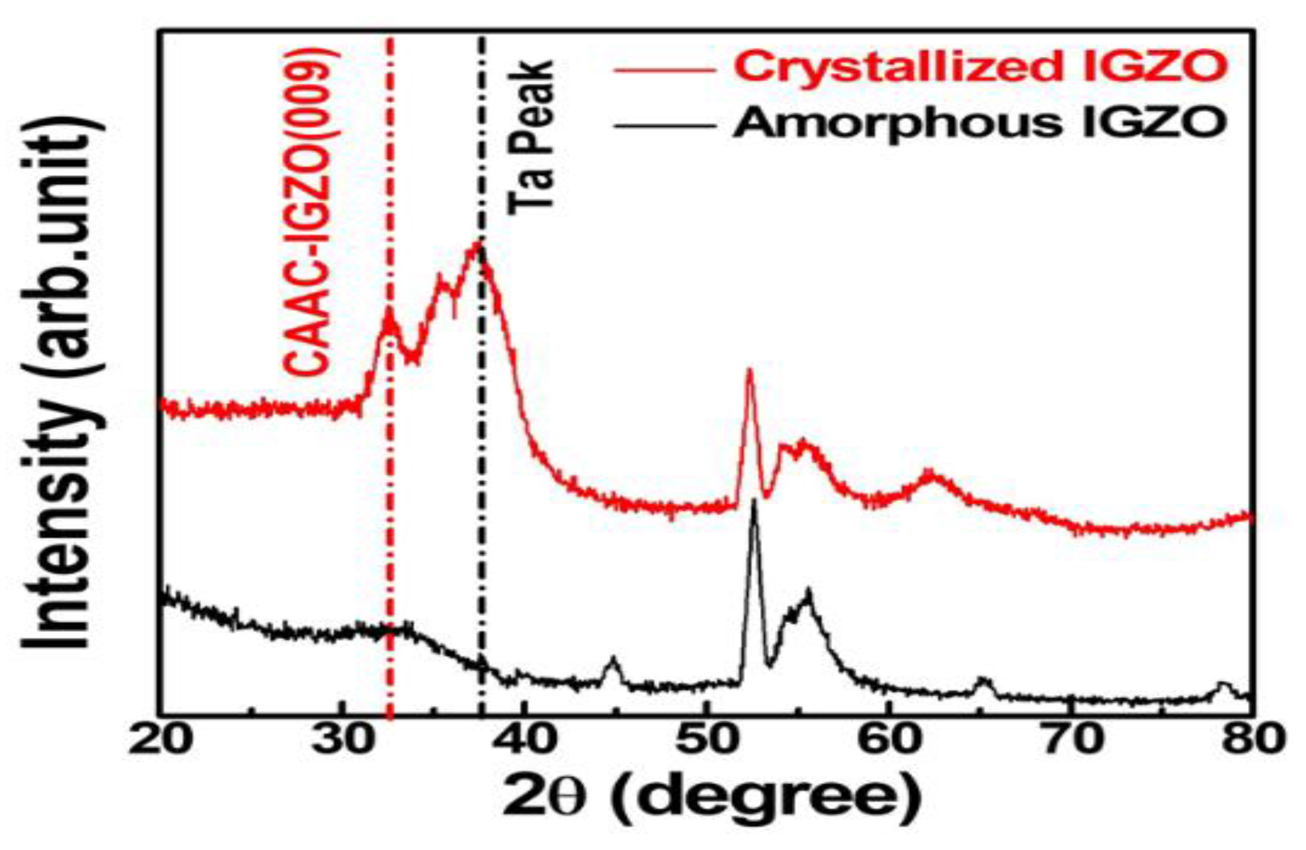
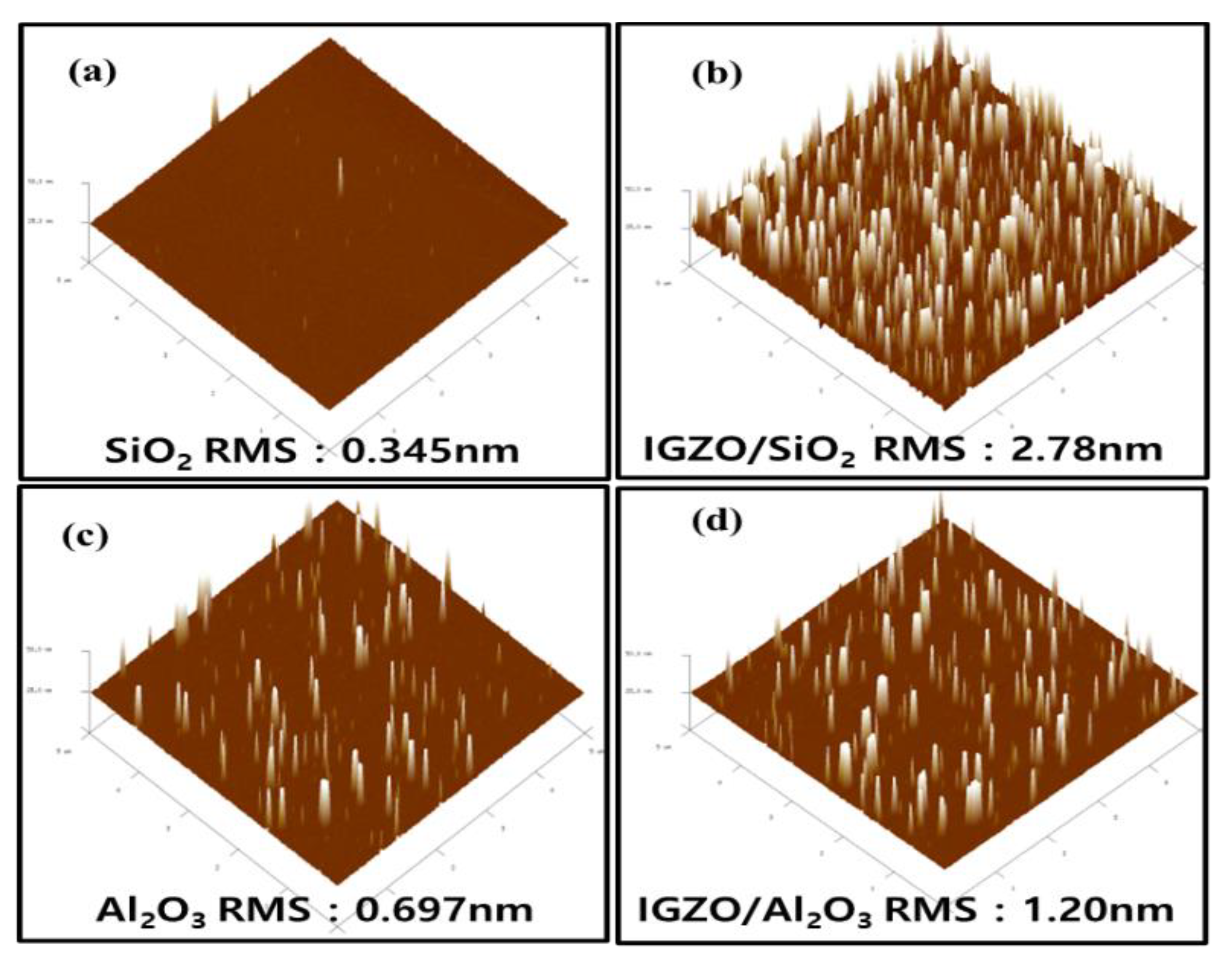
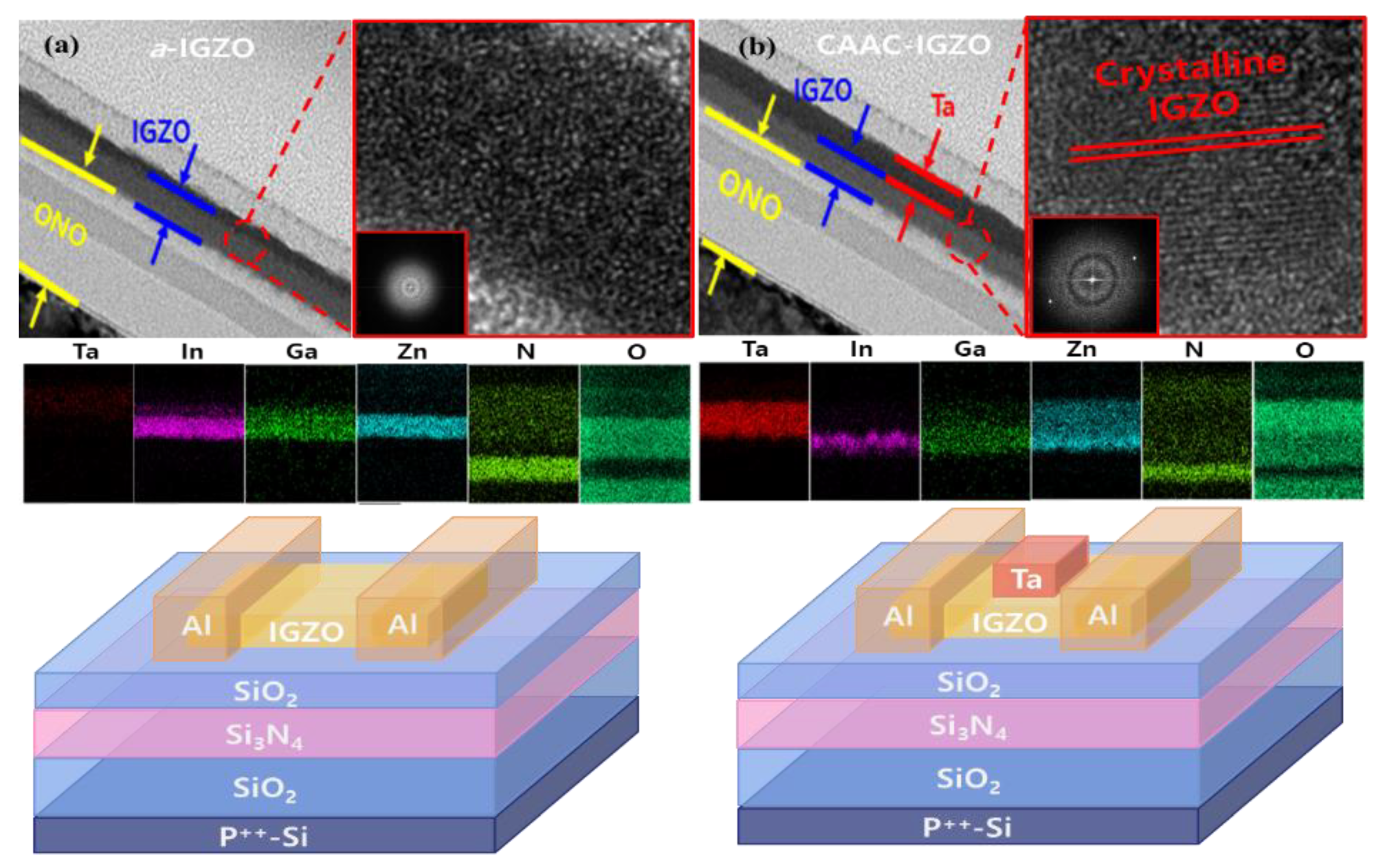
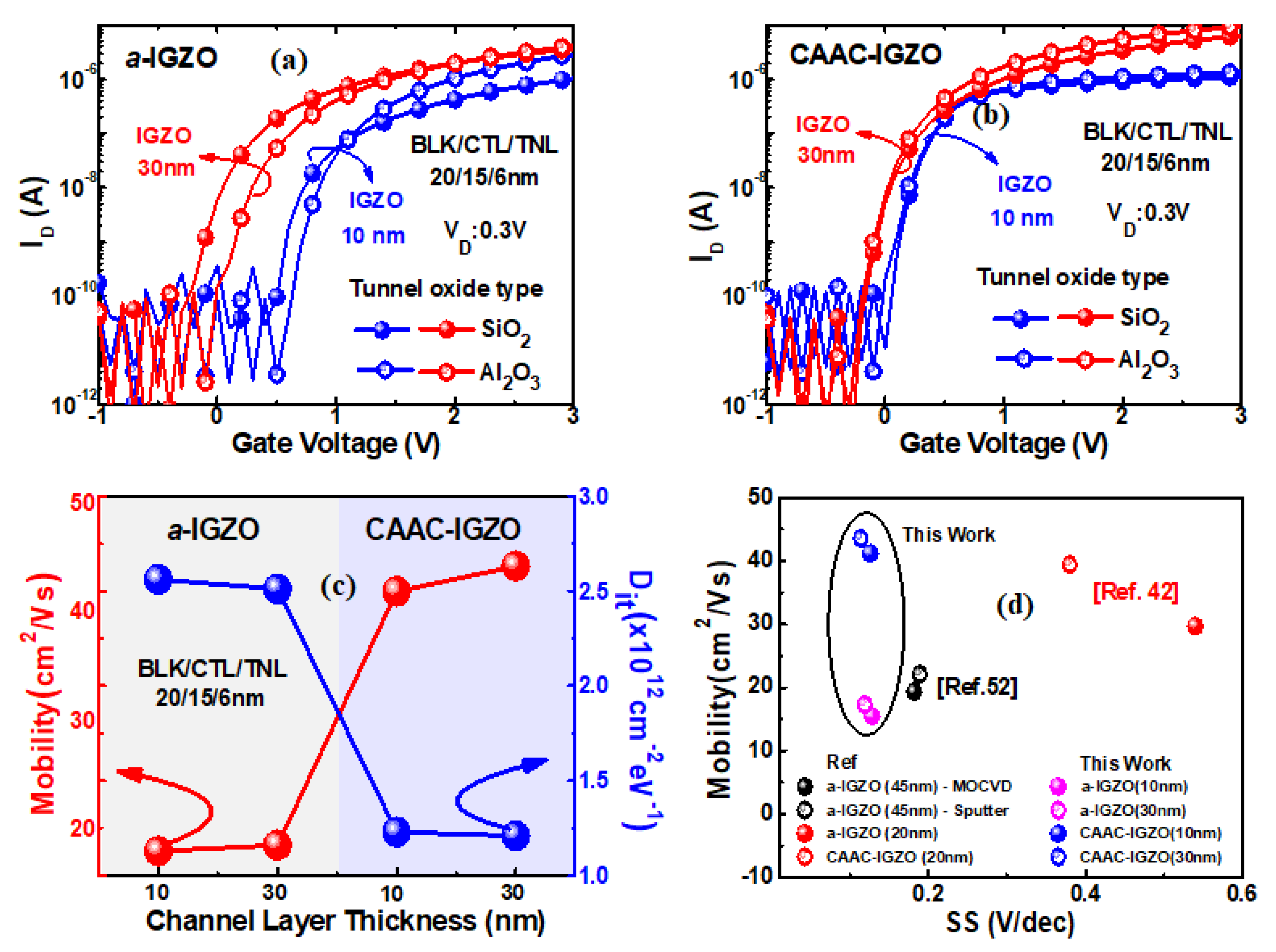
3. Results and Discussion

Figure 1 compares the XRD spectra for IGZO crystallization between a-IGZO and CAAC-IGZO. The Ta-capped IGZO film has two distinct peaks, and a crystallized IGZO (009) XRD peak was detected near 32°; however, no peak was observed in the case of a-IGZO. The XRD peak near 38.5° corresponds to the tetragonal b-Ta metal layer (110) [42].
Figure 2 shows the surface roughness images of IGZO on the SiO2 or Al2O3 layers using an atomic force microscope (AFM). In the TFT flash memory device structure, because the active IGZO layer was formed on TNL, SiO2, and Al2O3, it was necessary to check the surface roughness. The surface roughness of the SiO2 layer was smoother than that of Al2O3 before a-IGZO deposition [43,44]. However, when a-IGZO was deposited, the surface roughness of SiO2 and Al2O3 increased from 0.345 to 2.78 nm and from 0.697 to 1.20 nm, respectively; however, Al2O3 was less rough than a-IGZO/SiO2. As previously reported, the Al2O3 film containing crystalline material is stable in a-IGZO because of the low defect concentration; however, the SiO2 film containing amorphous material has more defects [43].
Figure 3a,b show the TEM and structural images of flash memory devices with a-IGZO and CAAC-IGZO channel materials, respectively. Compared with the a-IGZO layer, the crystalline domains appear clearly within the CAAC-IGZO layer with the Ta catalyst layer, indicating that Ta atoms can induce atomic rearrangement in the a-IGZO layer and convert to the CAAC-IGZO layer. The EDS profile shows the atomic content through the structure, where the Ta atoms remain in their original state without penetration. In addition, the oxygen distributed in the crystallization process by the Ta metal layer in the IGZO layer was confirmed. Therefore, a good interface with stable crystalline IGZO was obtained, and it was expected that high-performance TFTs could be formed and good flash memory behavior achieved.
Figure 4 compares the characteristics of the a-IGZO TFT flash memory devices with ONO and ONA. The energy band diagrams of each case are shown in Figure 4a. A memory window via a change in threshold voltage (ΔVth) was obtained by adjusting a program voltage of 20 V and a program pulse time (1 ms to 100 ns) in a back gate transistor-based flash device (ONO and ONA: 20/15/6 nm). A more effective Vth change was obtained when Al2O3 was used as a TNL with a low bandgap compared with that of SiO2, as shown in Figure 4b,c. This superiority of Al2O3 to SiO2 was confirmed at the interface and in the operating performance of the flash device [45] because Al2O3 has greater electron affinity and a lower band gap [42], which contributes to easy passage of the carriers through the barrier.
For the performance evaluation of the a-IGZO and CAAC-IGZO devices, the transfer characteristic (Id-Vg) was compared, as shown in Figure 5. Different thicknesses (10 and 30 nm) of the active channel layer and tunneling oxide type (SiO2 and Al2O3) were used. Compared with the a-IGZO device shown in Figure 5a, the CAAC-IGZO device exhibited improved mobility, lower interface state density (Dit), and better Vth stability with the active layer thickness (Figure 5b). These characteristics were attributed to less oxygen vacancy in the crystallized IGZO than in a-IGZO [22,46,47,48,49,50]. These results indicate that the crystallinity of the channel material is an important parameter to enhance device performance. In addition, the device performance is also affected by the active layer thickness and tunneling oxide. Figure 5c compares the mobility and Dit for both devices. For the a-IGZO device, an the field effect mobility (µFE) was approximately 17 cm2/Vs for the IGZO thickness range from 10 to 30 nm. Alternatively, the CAAC-IGZO device has an µFE of approximately 43 cm2/Vs for the same thickness range. The crystallized channel could effectively suppress the subthreshold swing (SS) degradation. The Dit of the a-IGZO device was 2.5 × 1012 cm−2ev−1, whereas that of the CAAC-IGZO device was 1.2 × 1012 cm−2ev−1, where Dit was extracted from the SS value [51]. This improvement of the proposed CAAC-IGZO device structure was similar to other reported crystalline IGZO channel-based devices [42]. Figure 5d compares the device parameters of the mobility and SS in our devices with previously reported devices. The crystallized IGZO shows an improvement over a-IGZO and our materials show better enhancement than the other crystallized IGZO materials. The crystallization is also helpful to improve the interface quality.
For program characteristic between two devices, various measurement conditions were applied, as shown in Figure 6. These devices have SiO2 and Al2O3 as a TNL, and the film thickness was reduced from 20/15/6 nm to 5/7/5 nm for BKL/CTL/TNL. Using ONO thin films, compared with the a-IGZO device, a slightly wider Vth shift was attained using the CAAC-IGZO device even for different measurement pulse widths, as shown in Figure 6a,b. The Vth shift values were 0.66 and 0.74 V under a 100 μs pulse width for amorphous and crystallized devices, respectively, and the difference increased as the pulse width was reduced. Using Al2O3 as a TNL, better programming behavior was achieved. Compared to the device using SiO2 as a TNL, when Al2O3 was used as TNL, the a-IGZO device improved the programming characteristics by 28~35% and CAAC-IGZO device by 30–36%, and the crystallized channel device was still superior to the amorphous channel device. This advantage occurs because the fast carrier mobility can easily trap electrons in the CTL [42]. Figure 6c compares the programming characteristic with channel materials and TNL type with respect to the pulse width from 10−6 to 10−3 s at a 20 V programing voltage. The active layer crystallization and adoption of Al2O3 as a TNL clearly improved the programing characteristics.
ITO and Al were used for S/D regions to improve the memory window of the IGZO-based flash memory device. Using capacitor devices, we demonstrated that the flash operation depends on the S/D contact metals, as shown in Figure 7. Compared with ITO metal, the flat band voltage shift (C–V shift) was enhanced using the Al metal contact in the capacitor device, as shown in Figure 7b,d. This wider memory window was attributed to different band gap properties of the metal and IGZO layers. Figure 7a,c shows the corresponding energy band diagram of the corresponding capacitors with different metal contacts and IGZO active material. The barrier of the IGZO/metal (ITO [53] and Al [54]) can block the electron sinking from IGZO to the metal under pulse conditions; as a result, the Al metal contact can easily make electrons sink because of its lower electron affinity than that of IGZO [42]. Thus, the S/D contact metal is also an important parameter to increase the performance of IGZO-based flash memory with an Al2O3 TNL and the crystallized active channel material.
Based on the findings of the effect of S/D metal contact, the memory window was also studied in a back gate TFT. Figure 8 shows transfer characteristics of amorphous and crystallized IGZO-based flash memory with a S/D contact of ITO and Al metal. Figure 8a,c show a-IGZO devices with ITO and Al, respectively, while Figure 8b,d how CAAC-IGZO devices with ITO and Al, respectively. The TNL is Al2O3 and the active layer thickness is 15 nm. The flash memory operation properties with a-IGZO and CAAC-IGZO active layers were attained by applying a VPROG/ERASE pulse of ±18 V range for 1 ms for VD = 0.3 V. For both devices with Al for a S/D contact, a Vth shift was observed; however, a larger window occurred for the CAAC-IGZO device. The Vth shift of the amorphous and crystallized active channel devices were 0.28 and 0.4 V, respectively. However, the a-IGZO and CAAC-IGZO devices with ITO for a S/D contact had a negligible or narrower memory window than the Al for a S/D contact metal even though a higher VPROG/ERASE pulse of ±20 V for 1 ms was applied, as shown Figure 8a,b. This result suggests that the S/D contact metal significantly influences the flash memory operation.
Reliability characteristics, such as endurance and retention, were investigated to determine if the crystallized IGZO active channel material maintains its superiority over amorphous IGZO material. Figure 9 shows the retention characteristics for amorphous and crystallized IGZO channel devices using Al2O3 as TNL. Figure 9a,b corresponds to the retention behaviors of the a-IGZO and CAAC-IGZO channel devices, respectively, where the charge loss state was tested for up to 104 s. The memory window of the CAAC-IGZO device was wider and more stable than that of the a-IGZO device, indicating that the CAAC-IGZO active channel was quite stable. The charge of the a-IGZO-based flash memory can easily be lost at low bias. The a-IGZO and CAAC-IGZO-based devices were expected to have charge loss degradation of 39% and 65%, respectively, over 10 years from their pristine state. As previously reported, the crystallized IGZO-based flash memory retention can suppress the charge loss more than the amorphous IGZO channel device [42].
The endurance characteristics of the amorphous and crystallized IGZO channel devices up to 104 cycles are shown in Figure 10a,b, respectively. Both devices increased in terms of Vth shift during the program and erase pulse cycling. However, the endurance degradation of the crystallized IGZO device was less than that of the amorphous IGZO device. Similar to the retention behavior, the crystallized active layer provides more suitable memory properties than the amorphous layer.

4. Conclusions

In summary, we demonstrated a metal-induced c-axis crystallized IGZO-based flash memory with excellent performance compared with an a-IGZO device. The CAAC-IGZO layer shows improved μFE, SS, and Ion. In conjunction with Al2O3 as the TNL and Al as the S/D metal, the CAAC-IGZO flash memory exhibits a wider memory window and superior endurance and retention characteristics, indicating that crystallized IGZO may be an alternative channel material for advanced flash memory device applications.

Author Contributions

Methodology, paper writing, investigation, conceptualization, H.H.; Validation, S.J., D.K., T.K., H.C., H.S.; funding acquisition, supervision and editing, C.C. All authors have read and agreed to the published version of the manuscript.

Funding

This work supported by the Future Semiconductor Device Technology Development Program (10080689, 20003808, 20004399) funded by MOTIE (Ministry of Trade, Industry & Energy) and KSRC (Korea Semiconductor Research Consortium), This research was supported by the BK21 FOUR (Fostering Outstanding Universities for Research) project of the National Research Foundation of Korea Grant.

Conflicts of Interest

The authors declare no conflict of interest.

References

  1. Lue, H.T.; Lai, S.C.; Hsu, T.H.; Hsiao, Y.H.; Du, P.Y.; Wang, S.Y.; Hsieh, K.Y.; Liu, R.; Lu, C.Y. A critical review of charge-trapping NAND flash devices. In Proceedings of the 2008 9th International Conference on Solid-State and Integrated-Circuit Technology, Beijing, China, 20–23 October 2008; p. 4734663. [Google Scholar]
  2. Zhao, C.; Zhao, C.Z.; Taylor, S.; Chalker, P.R. Review on non-volatile memory with high-k dielectric: Flash for generation beyond 32 nm. Materials 2014, 7, 5117–5145. [Google Scholar] [CrossRef] [Green Version]
  3. Ramkumar, K.; Prabhakar, V.; Keshavarzi, A.; Kouznetsov, I.; Geha, S. SONOS memories: Advances in materials and devices. MRS Adv. 2017, 2, 209–221. [Google Scholar] [CrossRef]
  4. Compagnoni, C.M.; Goda, A.; Spinelli, A.S.; Feeley, P.; Lacaita, A.L.; Visconti, A. Reviewing the evolution of the NAND flash technology. Proc. IEEE 2017, 105, 1609. [Google Scholar] [CrossRef]
  5. Nomura, K.; Ohta, H.; Takagi, A.; Kamiya, T.; Hirano, M.; Hosono, H. Room-temperature fabrication of transparent flexible thin-film transistors using amorphous oxide semiconductors. Nature 2004, 432, 488–492. [Google Scholar] [CrossRef]
  6. Jianhen, S.; Hong, T.; Lee, H.-M.; Kim, K.; Sasase, M.; Kim, J.; Hosono, H.; Park, J.-S. Amorphous IGZO TFT with High Mobility of ~70 cm2/(Vs) via Vertical Dimension. ACS Appl. Mater. Interfaces 2004, 11, 40300–40309. [Google Scholar]
  7. Oota, M.; Ando, Y.; Tsuda, K.; Koshida, T.; Oshita, S.; Suzuki, A.; Fukushima, K.; Nagatsuka, S.; Onuki, T.; Hodo, R.; et al. 3D-stacked CAAC-In-Ga-Zn Oxide Fets with Gate Length of 72 nm. In Proceedings of the 2019 IEEE International Electron Devices Meeting (IEDM), San Francisco, CA, USA, 7–11 December 2019. [Google Scholar]
  8. Wu, K.; Zhang, J.; Li, Y.; Wang, X.; Liu, Y.; Yu, Q.; Chen, T. Design of AM Self-Capacitive Transparent Touch Panel Based on a-IGZO Thin-Film Transistors. IEEE Access 2020, 2989435, 76929–76934. [Google Scholar] [CrossRef]
  9. Cho, M.H.; Choi, C.H.; Seul, H.J.; Cho, H.C.; Jeong, J.K. Achieving a Low-Voltage, High-Mobility IGZO Transistor through and ALD-Derived Bilayer Channel and a Hafnia-Based Gate Dielectric Stack. ACS Appl. Mater. Interfaces 2021, 13, 16628–16640. [Google Scholar] [CrossRef] [PubMed]
  10. Samanta, S.; Chand, U.; Xu, S.; Han, K.; Wu, Y.; Wang, C.; Kumar, A.; Velluri, H.; Li, Y.; Fong, X.; et al. Low Subthreshold Swing and High Mobility Amorphous Indium-Gallium-Zinc-Oxide Thin-Film Transistor with Thin HfO2 Gate Dielectric and Excellent Uniformity. IEEE Electron Device Lett. 2020, 41, 856–859. [Google Scholar] [CrossRef]
  11. Chu, Y.L.; Young, S.-J.; Ji, L.-W.; Yan, S.-P. Fabrication and Characterization of a-IGZO Thin-Film Transistors with and without Passivation Layers. ECS J. Solid State SCI. Technol. 2021, 10, 027002. [Google Scholar] [CrossRef]
  12. Jeon, S.; Ahn, S.-E.; Song, I.; Kim, C.J.; Chung, U.-I.; Lee, E.; Yoo, I.; Nathan, A.; Lee, S.; Ghaffarzadeh, K.; et al. Gated three-terminal device architecture to eliminate persistent photoconductivity in oxide semiconductor photosensor arrays. Nat. Mater. 2012, 11, 301–305. [Google Scholar] [CrossRef] [PubMed]
  13. Yu, Y.; Lv, N.; Zhang, D.; Wei, Y.; Wang, M. High-Mobility Amorphous InGaZnO Thin-Film Transistors with Nitrogen Introduced Via Low-Temperature Annealing. IEEE Electron Device Lett. 2021, 42, 1480–1483. [Google Scholar] [CrossRef]
  14. Koretomo, D.; Shuhei, H.; Marin, M.; Yusaku, M.; Mamoru, F. Marked improvement in reliability of 150 °C processed IGZO thin-film transistors by applying hydrogenated IGZO as a channel material. Appl. Phys. Express 2020, 13, 076501. [Google Scholar] [CrossRef]
  15. Cho, M.H.; Seol, H.; Song, A.; Choi, S.; Song, Y.; Yun, P.S.; Chung, K.-B.; Bae, J.U.; Park, K.-S.; Jeong, J.K. Comparative Study on Performance of IGZO Transistors With Sputtered and Atomic Layer Deposited Channel Layer. IEEE Trans. Electron Devices 2019, 66, 1780–1788. [Google Scholar] [CrossRef]
  16. Mo, F.; Tagawa, Y.; Jin, C.; Ahn, M.; Saraya, T.; Hiramoto, T.; Kobayashi, M. Low-Voltage Operating Ferroelectric FET with Ultrathin IGZO Channel for High-Density Memory Application. IEEE J. Electron Devices Soc. 2020, 8, 717–723. [Google Scholar] [CrossRef]
  17. Shi, L.; Wang, J.; Zhang, Y. Synergistic improvement of device performance and bias stress stability of IGZO TFT via back-channel graded nitrogen doping. Mater. Lett. 2021, 305, 130749. [Google Scholar] [CrossRef]
  18. Kim, Y.S.; Lee, M.-H.; Lim, J.H.; Park, J.-S. Impact of tandem IGZO/ZnON TFT with energy-band aligned structure. Appl. Phys. Lett. 2020, 117, 143505. [Google Scholar] [CrossRef]
  19. Park, C.B.; Na, H.I.; Yoo, S.S.; Park, K.-S. Electromechanical properties of amorphous indium-gallium-zinc-oxide transistors structured with an island configuration on plastic. Appl. Phys. Express 2016, 9, 031101. [Google Scholar] [CrossRef]
  20. Kim, W.-G.; Tak, Y.J.; Ahn, B.D.; Jung, T.S.; Chung, K.-B.; Kim, H.J. High-pressure gas activation for amorphous indium-gallium-zinc-oxide thin-film transistors at 100 °C. Sci. Rep. 2016, 6, 23039. [Google Scholar] [CrossRef] [PubMed]
  21. Petti, L.; Munzenrieder, N.; Vogt, C.; Faber, H.; Buthe, L.; Cantarella, G.; Bottacchi, F.; Anthopoulos, T.D.; Troster, G. Metal oxide semiconductor thin-film transistor for flexible electronics. Appl. Phys. Rev. 2016, 3, 021303. [Google Scholar] [CrossRef] [Green Version]
  22. Shin, Y.; Kim, S.T.; Kim, K.; Kim, M.Y.; Oh, S.; Jeong, J.K. The mobility enhancement of indium gallium zinc oxide transistors via low-temperature crystallization using a tantalum catalytic layer. Sci. Rep. 2017, 7, 10885. [Google Scholar] [CrossRef] [PubMed]
  23. Suzuki, A.; Yuichi, Y.; Mizukami, S.; Tsuda, K.; Ito, M.; Ohchima, K.; Matsumoto, N.; Yakubo, Y.; Miyata, S.; Okuno, N.; et al. Characteristics and Application of CAAC-IGZO FET with Gate Length of 13 nm. ECS Trans. 2020, 98, 13–27. [Google Scholar] [CrossRef]
  24. Kato, K.; Shionoiri, Y.; Sekine, Y.; Furutani, K.; Hatano, T.; Aoki, T.; Sasaki, M.; Tomatsu, H.; Koyama, J.; Yamazaki, S. Evaluation of off-state current characteristics of transistor using oxide semiconductor material, indium-gallium-zinc oxide. Jpn. J. Appl. Phys. 2012, 5, 021201. [Google Scholar] [CrossRef]
  25. Kobayashi, Y.; Matsudo, S.; Matsubayashi, D.; Suzawa, H.; Sakakura, M.; Hanaoka, K.; Okazaki, Y.; Yamamoto, T.; Hondo, S.; Hamada, T.; et al. Electrical characteristics and short-channel effect of c-axis aligned crystal indium gallium zinc oxide transistor with short channel length. Jpn. J. Appl. Phys. 2014, 53, 04EF03. [Google Scholar] [CrossRef]
  26. Kang, Y.; Lee, W.; Kim, J.; Keum, K.; Kang, S.-H.; Jo, J.-W.; Park, S.K.; Kim, Y.-H. Effects of crystalline structure of IGZO thin films on the electrical and photo-stability of metal-oxide thin-film transistors. Mater. Res. Bull. 2021, 139, 111252. [Google Scholar] [CrossRef]
  27. Kurokawa, Y.; Aoki, T.; Kozuma, M.; Kimura, H.; Kanemura, T.; Ando, Y.; Yamazaki, S. CAAC-IGZO FET/Si-FET hybrid structured analog multiplier and vector-by-matrix multiplier for neural network. Jpn. J. Appl. Phys. 2020, 59, SGGB03. [Google Scholar] [CrossRef]
  28. Yamazaki, S.; Atsumi, T.; Dairiki, K.; Okazaki, K.; Kimizuka, N. In-Ga-Zn-Oxide semiconductor and its transistor characteristics. ECS J. Solid State Sci. Technol. 2014, 3, Q3012–Q3022. [Google Scholar] [CrossRef]
  29. Yamazaki, S.; Yamazaki, S.; Suzawa, H.; Inoue, K.; Kato, K.; Hirohashi, T.; Okazaki, K.; Kimizuka, N. Properties of crystalline In-Ga-Zn-oxide semiconductor and its transistor characteristics. Jpn. J. Appl. Phys. 2014, 53, 04ED18. [Google Scholar] [CrossRef]
  30. Wang, X.; Shen, Z.; Li, J.; Wu, S. Preparation and Properties of Crystalline IGZO Thin Films. Membrane 2021, 11, 134. [Google Scholar] [CrossRef] [PubMed]
  31. Kunitake, H.; Ohshima, K.; Tsuda, K.; Matsumoto, N.; Koshida, T.; Ohshita, S.; Sawai, H.; Yanagisawa, Y.; Saga, S.; Arasawa, R.; et al. A C-Axis-Aligned Crystalline In-Ga-Zn Oxide FET with a Gate Length of 21 nm Suitable for Memory Applications. IEEE J. Electron Devices Soc. 2019, 7, 495–502. [Google Scholar] [CrossRef]
  32. Setten, M.J.V.; Dekkers, H.F.W.; Kljucar, L.; Mitard, J.; Pashartis, C.; Subhechha, S.; Rassoul, N.; Delhougne, R.; Kar, G.S.; Pourtois, G. Oxygen Defect Stability in Amorphous, C-Axis Aligned, and spinel IGZO. ACS Appl. Electron. Mater. 2021, 3, 4037–4046. [Google Scholar] [CrossRef]
  33. Hwang, A.Y.; Kim, S.T.; Ji, H.; Shin, Y.; Jeong, J.K. Metal-induced crystallization of amorphous zinc tin oxide semiconductors for high mobility thin-film transistors. Appl. Phys. Lett. 2016, 108, 152111. [Google Scholar] [CrossRef]
  34. Zhang, J.; Wen, X.; Hu, L.; Xu, W.; Zhu, D.; Cao, P.; Liu, W.; Han, S.; Liu, X.; Jia, F.; et al. C-axis oriented crystalline IGZO thin-film transistors by magnetron sputtering. J. Mater. Chem. C 2017, 5, 2388. [Google Scholar] [CrossRef]
  35. Kurokawa, Y.; Okamoto, Y.; Nakagawa, T.; Aoki, T.; Ikeda, M.; Kozuma, M.; Osada, T.; Ikeda, T.; Yamade, N.; Okazaki, Y.; et al. Applications of crystalline indium-gallium-zinc-oxide technology to LSI: Memory, processor, Image sensor, and field programmable gate array. In Proceedings of the Fifth Asia Symposium on Quality Electronic Design (ASQED 2013), Penang, Malaysia, 26–28 August 2013. [Google Scholar]
  36. Kozuma, M.; Okamoto, Y.; Nakagawa, T.; Aoki, T.; Ikeda, M.; Osada, T.; Kurokawa, Y.; Ikeda, T.; Yamade, N.; Okazaki, Y.; et al. Crystalline In-Ga-Zn-O FET-based configuration memory for multi-context field-programmable gate array realizing fine-grained power gating. Jpn. J. Appl. Phys. 2014, 53, 04EF12. [Google Scholar] [CrossRef] [Green Version]
  37. Matsuzaki, T.; Onuki, T.; Nagatsuka, S.; Inoue, H.; Ishizu, T.; Ieda, Y.; Yamade, N.; Miyairi, H.; Sakakura, M.; Shionoiri, Y.; et al. A 16-level-cell memory with c-axis-aligned a-b-plane-anchored crystal In-Ga-Zn oxide FET using threshold voltage cancel write method. Jpn. J. Appl. Phys. 2016, 55, 04EE02. [Google Scholar] [CrossRef]
  38. Kandpal, K. A review of evolution comes in non-volatile semiconductor memories like SONOS with the role of high-k dielectric material. IOSR J. Eng. IOSRJEN 2014, 4, 13–17. [Google Scholar] [CrossRef]
  39. Lee, M.C.; Wong, H.Y. Threshold voltage instability mechanisms of nitride-based charge trap flash memory—A review. J. Nanosci. Nanotechnol. 2014, 14, 4799–4812. [Google Scholar] [CrossRef] [PubMed]
  40. Breuil, L.; Lisoni, J.G.; Blomme, P.; Van den Bosch, G.; Van Houdt, J. HfO2 based high-k inter-gate dielectrics for planar NAND flash memory. IEEE Electron Device Lett. 2014, 35, 45–47. [Google Scholar] [CrossRef]
  41. Tang, Z.; Liu, Z.; Zhu, X. Progress of high-k dielectric applicable to SONOS-type nonvolatile semiconductor memories. Trans. Electr. Electron. Mater. 2010, 11, 155–165. [Google Scholar] [CrossRef]
  42. Jeong, S.; Jang, S.; Han, H.; Kim, H.; Choi, C. C-axis aligned crystalline indium-gallium-zinc oxide (CAAC-IGZO) and high-k charge trapping film for flash memory application. J. Alloys Compd. 2021, 888, 161440. [Google Scholar] [CrossRef]
  43. Linfeng, L.; Peng, J. High-Performance Indium-Gallium-Zinc-Oxide thin-film transistors based on anodic aluminum oxide. Trans. Electron Device 2011, 58, 1452–1455. [Google Scholar] [CrossRef]
  44. Li, Q.; Yu, Y.-H.; Bhatia, C.S.; Marks, L.D.; Lee, S.C.; Chung, Y.W. Low-temperature magnetron sputter-deposition, hardness, and electrical resistivity of amorphous and crystalline alumina thin films. J. Vac. Sci. Technol. A Vac. Surf. Films 2000, 18, 2333–2338. [Google Scholar] [CrossRef] [Green Version]
  45. Fulton, C.C.; Lucovsky, G.; Nemanich, R.J. Electronic properties of the Zr-ZrO2-SiO2-Si(100) gate stack structure, J. Appl. Phys. 2006, 99, 063708. [Google Scholar] [CrossRef] [Green Version]
  46. Lee, C.B.; Kang, B.S.; Benayad, A.; Lee, M.J.; Ahn, S.-E.; Kim, K.H.; Stefanovich, G.; Park, Y.; Yoo, I.K. Effects of metal electrodes on the resistive memory switching property of NiO thin films. Appl. Phys. Lett. 2008, 93, 042115. [Google Scholar] [CrossRef]
  47. Nomura, K.; Kamiya, T.; Hosono, H. Highly stable amorphous In-Ga-Zn-O thin-film transistors produced by eliminating deep subgap defects. Appl. Phys. Lett. 2011, 99, 053505. [Google Scholar] [CrossRef]
  48. Zan, H.W.; Yeh, C.-C.; Meng, H.-F.; Tsai, C.-C.; Chen, L.-H. Achieving high field-effect mobility in amorphous indium-gallium-zinc oxide by capping a strong reduction layer. Adv. Mater. 2012, 24, 3509–3514. [Google Scholar] [CrossRef]
  49. Rajachidambaram, M.S.; Pandey, A.; Vilayurganapathy, S.; Nachimuthu, P.; Thevuthasan, S.; Herman, G.S. Improved stability of amorphous zinc tin oxide thin film transistors using molecular passivation. Appl. Phys. Lett. 2013, 103, 171602. [Google Scholar] [CrossRef]
  50. Robertson, J.; Guo, Y. Light induced instability mechanism in amorphous InGaZn oxide semiconductors. Appl. Phys. Lett. 2014, 104, 162102. [Google Scholar] [CrossRef]
  51. Ma, P.; Du, L.; Wang, Y.; Jiang, R.; Xin, Q.; Li, Y.; Song, A. Low voltage operation of IGZO thin film transistors enabled by ultrathin Al2O3 gate dielectric. Appl. Phys. Lett. 2018, 112, 023501. [Google Scholar] [CrossRef] [Green Version]
  52. Hwang, E.S.; Kim, J.S.; Jeon, S.M.; Lee, S.J.; Jang, Y.; Cho, D.Y.; Hwang, C.S. In2Ga2ZnO7 oxide semiconductor-based charge trap device for NA for NAND flash memory. Nanotechnology 2018, 29, 155203. [Google Scholar] [CrossRef]
  53. Lei, H.; Qin, P.; Ke, W.; Guo, Y.; Dai, X.; Chen, Z.; Wang, H.; Li, B.; Zheng, Q.; Fang, G. Performance enhancement of polymer solar cells with high work function CuS modified ITO as anodes. Org. Electron 2015, 22, 173–179. [Google Scholar] [CrossRef]
  54. Kumar, B.; Kauzhik, B.K.; Negi, Y.S. Perspectives and challenges for organic thin film transistors: Materials, devices, processes and applications. J. Mater. Sci. Mater. Electron. 2014, 25, 1–30. [Google Scholar] [CrossRef]
Figure 1. XRD spectra of the IGZO thin film without and with Ta metal film that was annealed at 300 °C under O2 ambient for 1 h.
Electronics 11 00053 g001
Figure 2. AFM images of (a) SiO2, (b) IGZO on SiO2, (c) Al2O3, and (d) IGZO on Al2O3 where SiO2 and Al2O3 serve as the TNL in the TFT flash memory device.
Electronics 11 00053 g002
Figure 3. Cross-sectional flash memory TEM images and device schemes with (a) a-IGZO and (b) CAAC-IGZO layers.
Electronics 11 00053 g003
Figure 4. Schematics of (a) the energy band diagrams of TFT flash memory devices with SiO2 and Al2O3 as the TNL. Programing behaviors under various pulse times for a-IGZO TFT flash memory devices with (b) SiO2 and (c) Al2O3 TNLs.
Electronics 11 00053 g004
Figure 5. Id–Vg comparison of the (a) a-IGZO and (b) CAAC-IGZO devices. (c) Dependence of the active layer thickness on µFE and Dit. (d) Comparison of reported IGZO-based devices with this work [42,52].
Electronics 11 00053 g005
Figure 6. Memory performance of devices using amorphous and crystallized IGZO active layers with different pulse conditions: (a) a-IGZO and (b) CAAC-IGZO. (c) Vth shift for different TNLs and program pulses.
Electronics 11 00053 g006
Figure 7. Schematics of energy diagrams: (a) a-IGZO/ITO and (c) a-IGZO/Al, C-V characteristic (b) a-IGZO/ITO and (d) a-IGZO/Al.
Electronics 11 00053 g007
Figure 8. Transfer characteristics of the a-IGZO and CAAC-IGZO devices with different S/D materials: (a,c) show a-IGZO devices with ITO and Al for S/D, respectively, and (b,d) show CAAC-IGZO devices with ITO and Al for S/D, respectively.
Electronics 11 00053 g008
Figure 9. Retention characteristics of (a) a-IGZO and (b) CAAC-IGZO devices tested up to 104 s.
Electronics 11 00053 g009
Figure 10. Endurance characteristics of (a) a-IGZO and (b) CAAC-IGZO devices tested up 104 cycles.
Electronics 11 00053 g010
Publisher’s Note: MDPI stays neutral with regard to jurisdictional claims in published maps and institutional affiliations.

