1. Introduction
With the substantial technological advancements, the potential for high conversion efficiency of crystalline silicon
solar cells. Photovoltaic
market dominated by crystalline silicon
solar cells [
1] by larger than
worldwide. The efficiency of
has been reached with
based modules and is continuously escalating both in the research and in the commercial market. Theoretically, the bandgap, long radiative recombination lifetimes, Auger recombination of the generated carriers restrict the conversion efficiency to about
[
2,
3,
4]. It is mandatory to reduce the various losses (optical, carrier, and electrical loss) in
solar cell to achieve the maximum conversion efficiency [
5]. One of the key issues of the contemporary PV industry is reducing the optical losses which make up about
efficiency loss in
solar cells [
6]. An approach to reduce the optical loss is to use an ARC at the front surface, which reduces the reflection losses and enhances the
consequently, improving the conversion efficiency. Several researchers employed various ARCs that might be used to increase the efficiency of the solar cell. Thin films such as
,
etc., were used as
layers [
7,
8,
9,
10,
11].
was a commonly used
on the front surface, owing to its versatility and inexpensive [
7]. Though
coatings possess better optical properties (high refractive index, low absorption coefficient) in the visible region, the passivation properties in addition to the optical properties made the
manufacturers shift to plasma-enhanced chemical vapour deposited
. In the recent study by various researchers,
films demonstrated the potential of delivering the exceptional passivation on boron-doped
emitters [
12,
13,
14].
is the ideal
material for the encapsulated cell as its
2.1 at the wavelength of
. In the earlier days of solar cell fabrication,
was considered only for
purposes. Later researchers found that
/
layers provided both surface passivation as well as
layers. Hence the solar cell industry utilizes the
/
layers. However recent research found the passivation properties especially provided better surface passivation with
surfaces. However, the change in its crystalline phase at higher temperatures hinders the application of
in conventional commercial solar cells fabrication, which requires high-temperature metallisation firing. Hence it might be considered. Thus, optimizing the
film with a trade-off between optical and passivation properties will be valuable for the
industry.
However, the single-layer
s
employed in silicon solar cells still instigate substantial optical reflectance loss in a wide-ranging of the solar spectrum. Thus, high-efficiency solar cells utilize double-layer ARCs
which improves the carrier collection by reducing the reflectance in the visible and in the near-IR range [
15,
16,
17,
18]. The
(
or
) is a favorable design to enhance the efficiency owing to its benefits in both antireflection and surface passivation properties. Doshi et.al. optimized the
film thickness and their refractive indices and utilized the
/
for their simulation [
15]. With
/
layer, Lennie et al. obtained an efficiency of
[
16] using Silvaco ATLAS simulation. Similar work with
simulation can be found elsewhere [
17,
18,
19].
is the most commercially accessible software utilized by several groups to simulate solar cells with unique
layers [
20]. In most of the
simulation studies, the maximum conversion efficiency of 3–13% only has been achieved [
16,
17,
18,
19].
In the present study, we employed the and on the actual industrial solar cell with a surface area of . Similarly, we analyzed the loss for each layer, to find the most optimum specification that can be employed for solar cell application. For , varying the thickness of the and its capping layer was one of the most novel concepts explored in this manuscript. This simulation-based approach highlighted in this manuscript plays a vital role in identifying the most optimal configuration of the layers for achieving increased efficiency of silicon solar cells. The simulation approach highly reduces the time and cost involved in testing the different combinations of layers and helps in identifying the optimal configuration of the layers. with different refractive indices were chosen as a capping layer when experimentally testing the layer. Mono-crystalline silicon solar cells were simulated using . The simulated device results were validated by comparing the solar cell fabricated with identical device parameters. This study offers a better insight into solar cell performance.
2. Simulation of Solar Cell
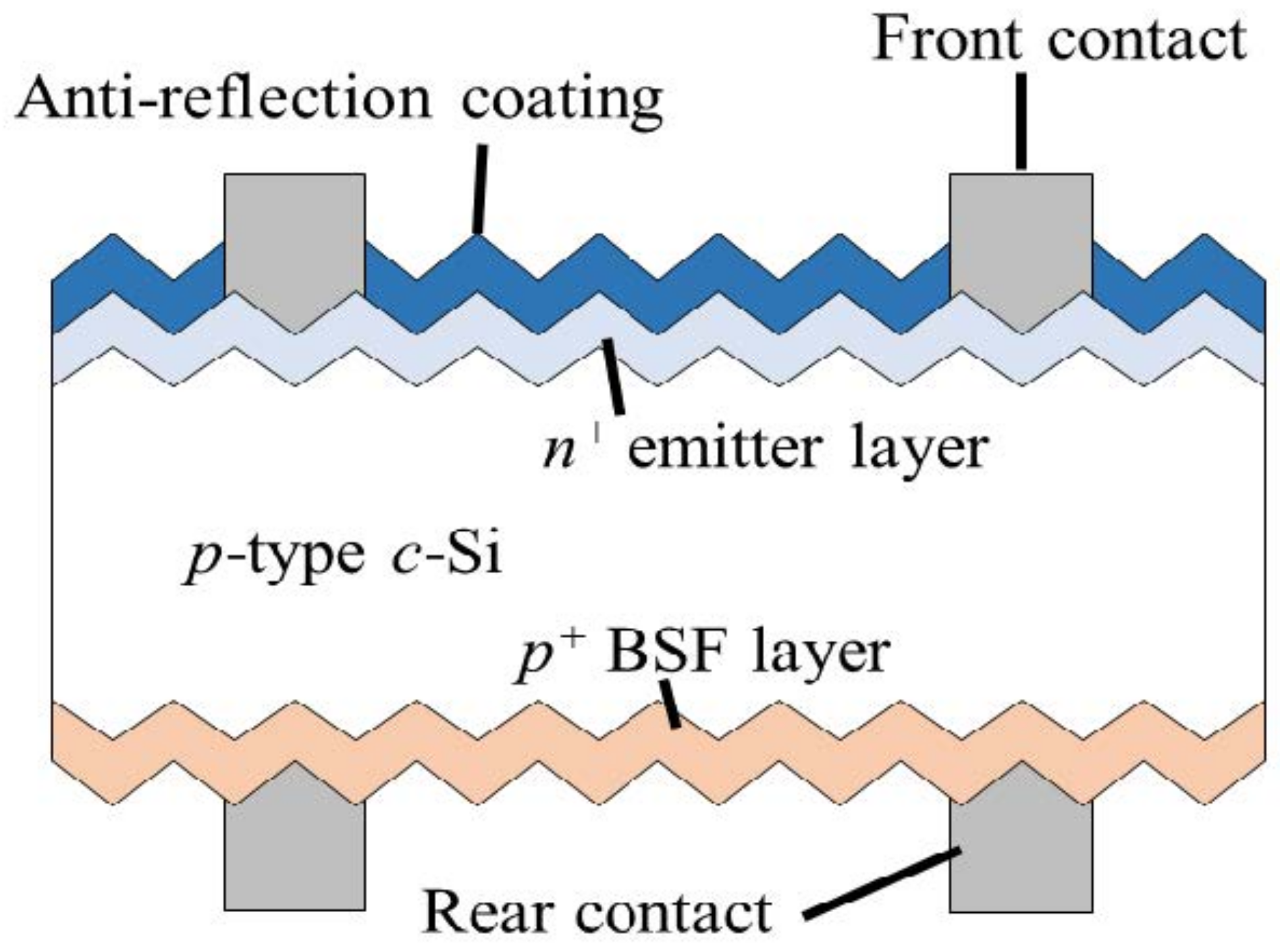
To simulate the
solar cell behaviour
software package is used in this study. The mathematical modelling tool used a more detailed silicon solar cell model as shown in
Figure 1. To increase the conversion accuracy of solar cells we need an accurate solar cell modelling tool. After studying each layer’s physical and electrical parameters of the
solar cell the
tool helps in studying the impact of various parameters considered in the fabrication of the solar cells. In this study, the actual device configuration for simulating and optimizing the anti-reflection coating
layer of solar cell is evaluated using
simulation and the optimized configuration for achieving higher accuracy is obtained. Using numerical modelling tools such as
to optimize the
layer configurations reduces the cost, time, and effort required to analyze the impact of the change in the design of the solar cells.
In the
simulation tool, crystalline Si (
) solar cell device simulations are carried out using the following numerical equations representing the quasi-one-dimensional transportation of electrons and holes of a semiconductor material (Solar cells). Equations (
1)–(
7) gives us a clear cut idea of creating a model of a silicon cell and optimizing various process parameters including the
coating layer properties [
21].
The current densities of the electrons and the holes are represented as
and
respectively and they are numerically formulated as indicated in Equations (
1) and (
2). In which, the parameters
n and
p are the electron and hole density,
and
is the mobility of the electron and holes. The
and
are the diffusion coefficients that represents the difference in electron and hole quasi-Fermi energies
and
.
Equations (
3) and (
4) are derived from the law of conservation of charge or the continuity equation. where
and
are generation rate and recombination rate. Equation (
5) represents Poisson’s equation for solving the electrostatic field problems. where
and
are acceptor and donor doping concentrations.
Here
and
are the effective density of states in the conduction and valence bands. To describe the type of material used, Fermi-Dirac statistics directly related to the band edges and
and
carrier densities are expressed in the Equations (
7) and (
8). The finite element approach is used to solve the three basic equations that assist in simulating the solar cell behaviours using the
modelling tool. Many other process parameters are optimized using the
simulation tool in the literature, but the proposed research aims to optimise the design process characteristics of the
layer used in the fabrication of the
solar cells. Finally, the efficiency of
solar cells is calculated using the following equations.
where,
represents the efficiency of the solar cell which is calculated using
,
,
,
,
,
and
that indicates the maximum power, incident power, current at maximum power point, voltage at maximum power point, saturation current density, Open circuit voltage and fill factor.
In this present study, we have considered p-type wafer with resistivity of 1 (doping of , device area of , front surface textured with 3 depth. The emitter and back surface field was formed with doping concentration of and respectively. Bulk lifetime of 100 and front and rear surface recombination velocity of 10,000 were considered for solar cell simulation by PC1D. Numerous simulations were performed to study the impact of different parameters on the solar cell device performance. Base resistance , internal conductance S), light intensity (0.1 were kept constant during simulation. spectrum was used in this modelling.
3. Results and Discussion
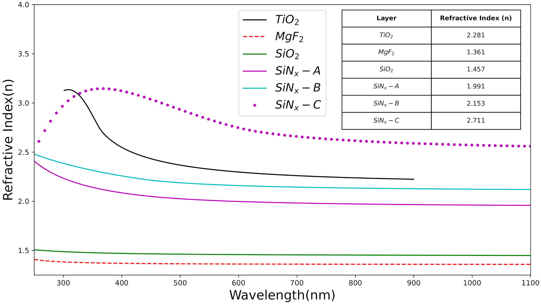
The refractive index as a function of wavelength defines the characteristics of an
layer [
22].
Figure 2 shows the wavelength dependent refractive indices of the
layers such as
[
14],
[
23],
[
24],
[
9] thin films determined using the spectroscopic ellipsometer. The inset of
Figure 2 shows the refractive index corresponding to each
layer. The refractive index values of the
and
C at
were about
, and
respectively.
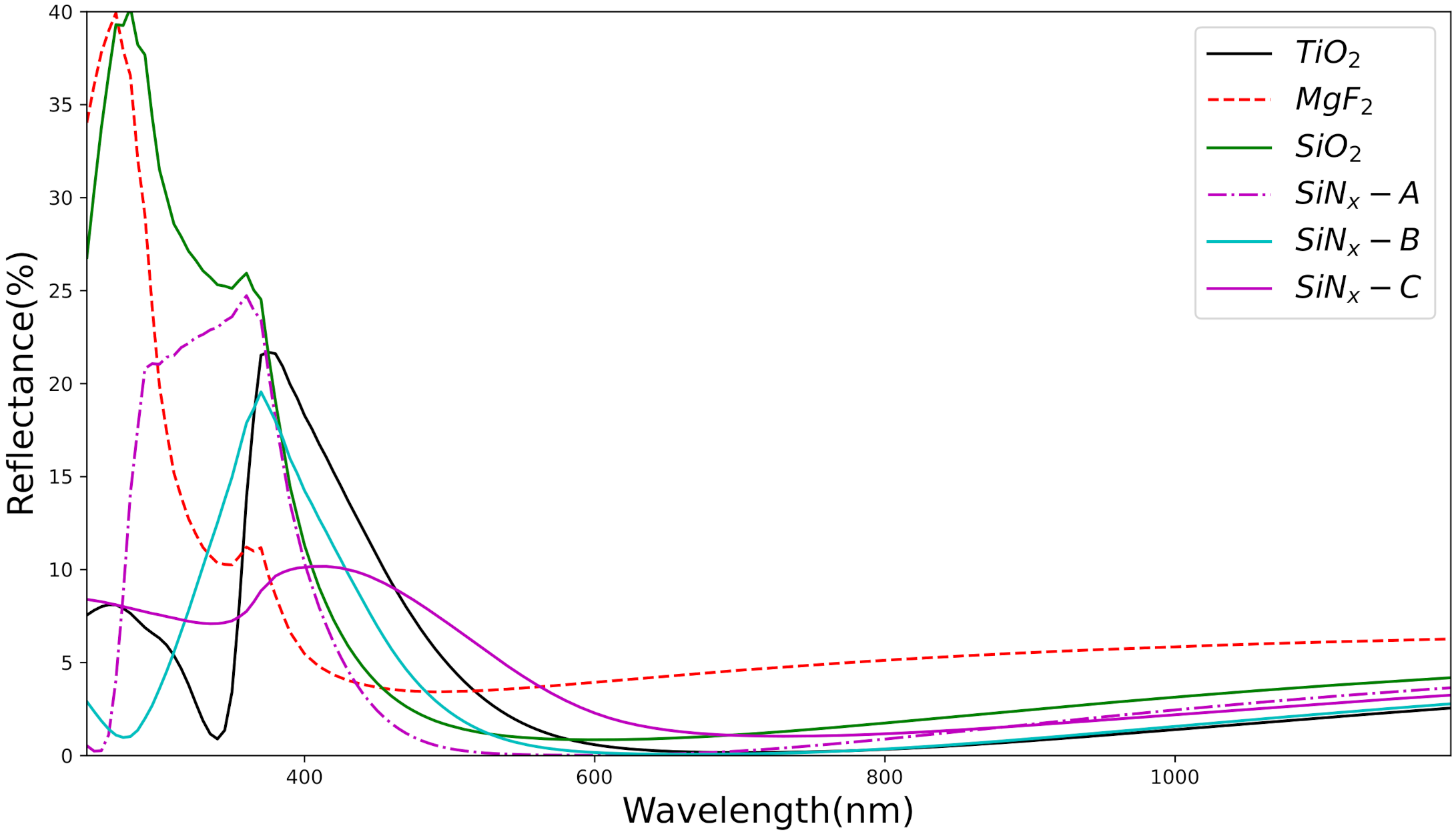
Reflectance spectra as a function of wavelength feed significant insights that can be used for investigating the optical properties of the
, textured surface, and internal reflectance at the rear surface of the solar cell device. An optimal
film for
solar cells should possess (i) low optical losses and (ii) provide good surface passivation. Reflectance spectra exhibit characteristic minima that are defined by the following equation:
where
t represents the thickness of the
,
represents the characteristic minimum wavelength, and
n represents the index of refraction. For each
layer with a different refractive index, the thickness of the
layer was varied from 70–100
to keep the optical thickness of the film constant.
Figure 3 shows the measured reflectance of the different
layers coated on the textured surface. These reflectance values were measured using
software. The
simulator was also used to optimise the layer thickness of the single/double-layer
coatings. The reflectance values were measured at the wavelength of
. The reflectance of
layers such as
and
are
,
and
respectively. Overall, the lowest reflectance value is for
and
layer, closely followed by
. Similar behaviour is observed in the case of saturation current density
.
Table 1 represents the
parameters as well as the calculated blue loss and
loss with different
layers
of
was obtained for
and
layer and
and
for
respectively. The
values obtained is in good agreement with the reflectance values of the
layers. Highest efficiency of
was obtained for the
layer with
and
. Current is one of the easiest factor that can be improved with substantial margin. Thus it is significant to enumerate systematically the source of
loss, breaking them into (i) optical losses and (ii) collection losses. The optical loss is due to metal shading, reflection and parasitic absorption and the collection losses arises due to imperfect emitter collection. By investigating the losses, it gives a clear representation of possible improvement areas which helps the PV manufacturers to predict and plan the strategies on the cell and module level fabrication for the future. Despite the well-known fact that the Mg-based
material is considered as the highly impactful material its associated drawback in terms of the
loss was highlighted and alternative materials
loss was evaluated and a detailed overview of the results was presented in
Table 2.
To explain the variation in the
with different
layers, the ARC loss was calculated by considering the
photon flux spectrum [
25] and internal quantum efficiency of the solar cell.
where
q is the elementary charge, lam
denotes the photon flux of the standard air mass solar spectrum between 300 to
is the reflectance and
is the internal quantum efficiency as a function of wavelength.
Reflection loss lead to a reduction of in for layers, for thermal and for layers with different refractive indices, thus decreasing the efficiency with respective ARC layers. The front metal coverage is not considered while calculating the values and hence, the variation. By considering the metal coverage area (4–7%), the calculated unshaded values is in good agreement with the measured .
This
loss may be reduced by tuning the
optical properties (e.g., refraction index and thickness), as well as through improved front surface texturing for better light-trapping. In general, the optical properties of the
materials are modified by replacing them with an alternate material to be used as the
material. One other alternate way of reducing the
loss is by optimizing the refractive indices of the
layer. In this study,
layers have been used with different refractive indices from
n = 1.99; 2.15 and 2.711 to analyse the impact of the material used as the
in the manuscript. From
Table 1 it is inferred that the
loss was higher for the
layers with the highest refractive indices, and it reduces significantly with a reduction in the refractive indices. The blue loss is the combined effect of
absorption, imperfect emitter collection, and front surface recombination.
-related blue loss may be reduced to a certain extent by tuning the
optical properties. Optimizing the emitter doping profile and junction depth can also help reduce emitter recombination losses. Front surface recombination can be reduced by improved front surface passivation.
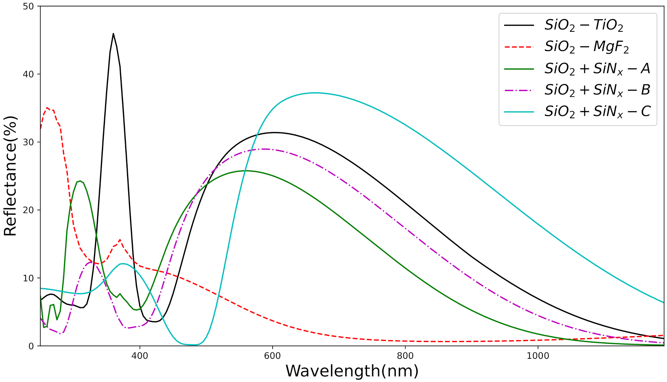
For further reduction in the reflectance, we considered the
.
Figure 4 depicts the reflectance spectra of various
layers. The
layer was capped with
and
layers. The thickness of the
layer and the capping layers were fixed as
and
respectively. The reflectance was higher for all the
layers and hence poor
values which are depicted in
Table 2. The high reflectance values for all the
layers are attributed to the unequal optical thickness of the
layer. The necessary and sufficient refractive index condition for a
with equal optical thickness to give zero reflectance is [
26]:
where
is the admittance of the surrounding medium.
Based on Equation (
11) the optical thickness of the
layers was optimized to obtain a minimum reflectance.
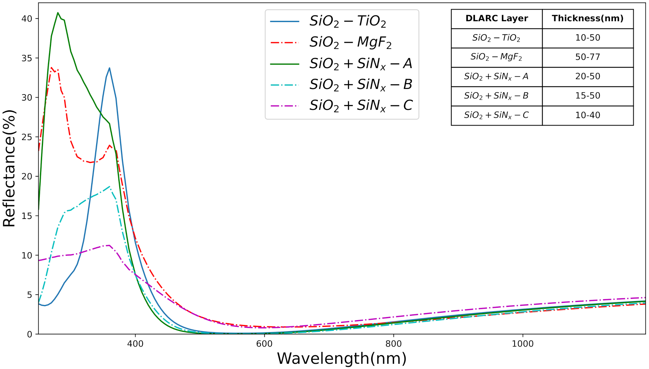
Figure 5 shows the reflectance spectra of the
layers. The inset of
Figure 6 shows the thickness variation for both
and the capping layer. The
layer capped with
and
showed a reflectance of
whereas for the
and
layers the reflectance was
and
respectively with the thickness of ∼60–70
. From the optimized reflectance curves, we can observe that when the reflectivity is substantially mitigated at the front surface, the gain in efficiency of the solar cell.
Table 3 represents the
parameters as well as the calculated blue loss and
loss with optimized
layers. With
, the
improved by ∼0.5
when the
was capped with
layer and hence the efficiency by
. It can be observed that the blue loss reduces significantly for the
compared with
. This reduction can be attributed to the effective passivation provided by the
layer. With
, the reflection loss reduced by
i.e., ∼1
in
compared with
.
Table 3.
parameters and loss calculation based on the optimized layers.
Table 3.
parameters and loss calculation based on the optimized layers.
| Layer |
(mA/cm2)
|
(mV)
|
| Eff
(%) | Blue Loss
(%) | ARC Loss
[%] | Unshaded
(mA/cm2)
|
|---|
| 38.29 | 654.2 | 82.42 | 20.65 | 0.13 | 1.03 | 40.13 |
| 38.11 | 654.1 | 82.43 | 20.55 | 0.13 | 1.42 | 39.74 |
| 38.41 | 654.3 | 82.42 | 20.72 | 0.13 | 0.83 | 40.34 |
| 38.52 | 654.4 | 82.42 | 20.78 | 0.13 | 0.67 | 40.49 |
| 38.16 | 654.1 | 82.42 | 20.57 | 0.13 | 1.03 | 40.13 |
Figure 5.
Reflectance spectra as a function of wavelength with optimized thickness of double-layer anti-reflection coating.
Figure 5.
Reflectance spectra as a function of wavelength with optimized thickness of double-layer anti-reflection coating.
Figure 6.
measurement carried on selected layers.
Figure 6.
measurement carried on selected layers.
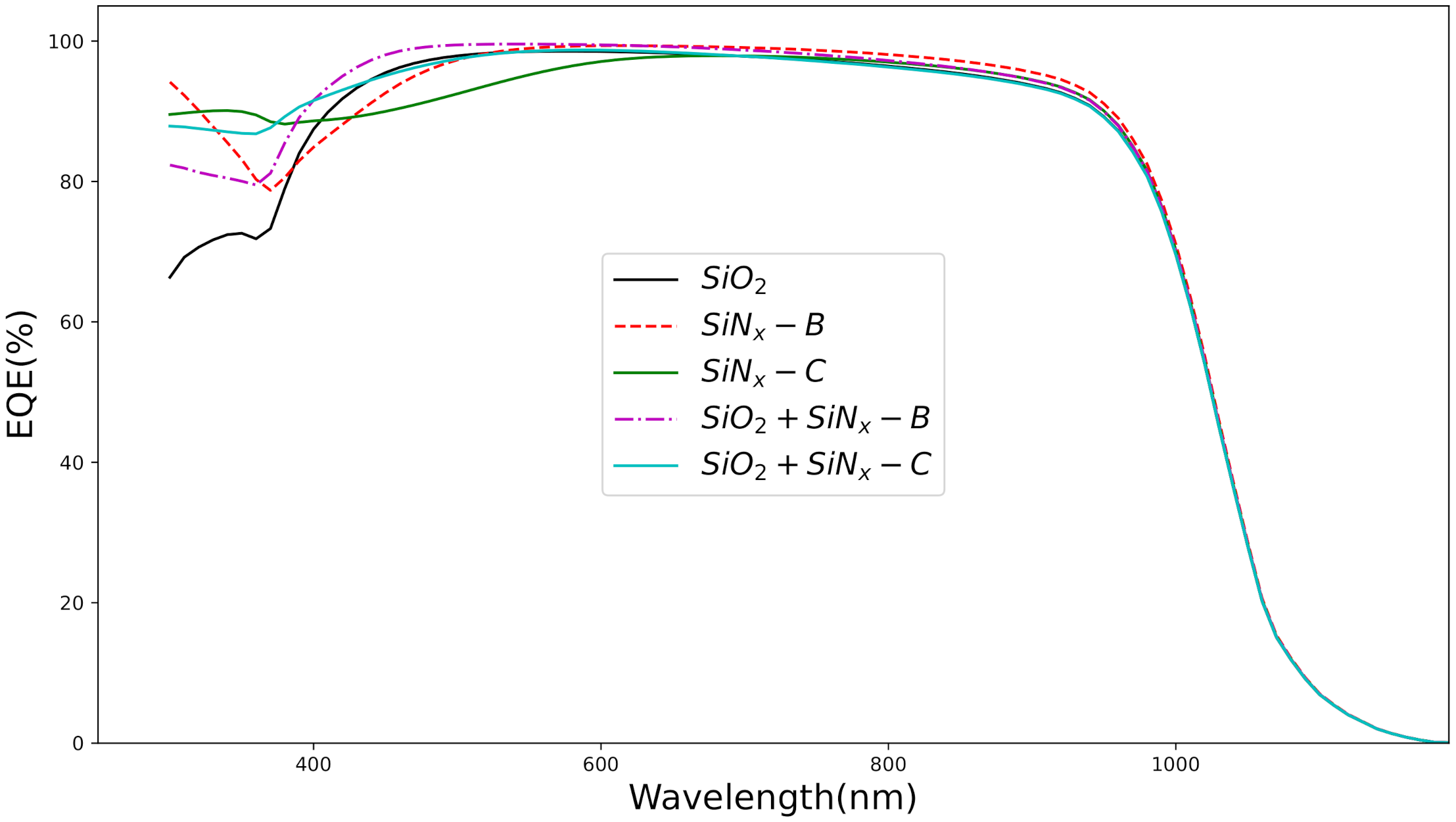
Figure 6 depicts the
obtained on the selected ARC layers.
of
layer showed a better blue response compared with
layers. However, the increase in
for the
layers is due to the better response i.e., more absorption in the long-wavelength region. From
Figure 6 it is obvious that with the utilization of the
layer, the carrier collection has improved significantly in the short wavelength range leading to the best conversion efficiency and
. This enhancement in
is attributed to the decrease in reflection with
. It is sufficient to say, this effective collection of carriers reduce the recombination at the interface, and hence the overall
is enhanced [
10].
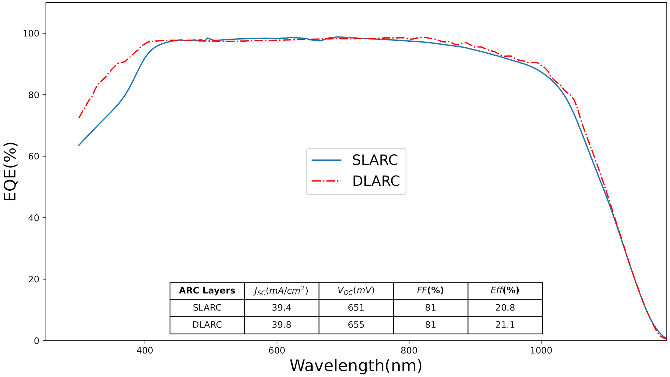
To validate the simulation data, a simulated device with identical parameters was compared to the measurements of actual solar cells in real application conditions. The industrial silicon solar cell was fabricated with both
and
.
thick
layer with the refractive index of
was used as
layer.
with
thick and
with
thick were used as
layer. The monocrystalline silicon solar cell showed the conversion efficiency of
and
shown in the inset of
Figure 7.
spectra indicate that the efficiency improvement for a solar cell with the
compared to the
. This improvement at the short wavelength region is vital and it’s attributed mainly to the role of the
. Thus, the
stacked layers reduce the reflection of high energy photons. In addition, the
layers provide better passivation thus enhancing the overall
by reducing the surface recombination at the interface. The efficiency of the solar cell using the optimized
layer settings is compared with the results obtained from the literature and presented in
Table 4. The result indicated that the identified
layer configuration outperforms the previously identified
and
layers highlighted in the literature.


 ,
, 


