Article

A Remedial Control for Short-Circuit Fault in NPC/H-Bridge Inverters without Redundant Component

1
Faculté des Sciences et Technologies, Campus Aiguillettes, Université de Lorraine, GREEN, F-54500 Nancy, France
2
Institut Jean Lamour (UMR7198), Département N2EV, Equipe Mesures et Architectures Électroniques (MAE), Université de Lorraine, CNRS, IJL, F-54500 Nancy, France
3
The Center of Excellence for Power Systems Automation and Operation, Department of Electrical Engineering, Iran University of Science and Technology, Tehran 1311416846, Iran
*
Author to whom correspondence should be addressed.
Electronics 2021, 10(19), 2411; https://doi.org/10.3390/electronics10192411
Submission received: 30 April 2021 / Revised: 22 September 2021 / Accepted: 24 September 2021 / Published: 2 October 2021

Abstract

:
In this paper, a five-level neutral-point-clamped (NPC) inverter with short-circuit fault-tolerant capability is presented. Based on the proposed approach, in order to ensure service continuity subsequent to a short-circuit fault event in a switch, two steps are carried out. First of all, destructive consequences arising from short-circuit fault in a power switch is prevented. Afterwards, according to the defected component, remedial actions are taken. The proposed strategy does not require any redundant component. The service continuity is acquired by applying a remedial control and modifying switching commands applied to the power switches. Using the proposed approach helps to restore the rated voltage and rated current at the terminal, and there is no limit for modulation index during fault-tolerant operation under remedial control. Furthermore, compared to healthy operation, harmonic content of the terminal voltage and current is not deteriorated during fault-tolerant operation. Moreover, additional components, such as bidirectional switches and contactors, are not employed in this strategy. Only some fast fuses are placed in the converter circuit for protection purposes which do not impose a noticeable cost compared to the bidirectional switches and contactors.

1. Introduction

Multilevel inverters have been extensively employed in industry for decades. Thanks to the significant advantages, such as less total harmonic distortion, less switching losses, limited voltage transients, reduced common-mode voltage, and small size of filter elements, multilevel inverters have become a worthy substitute for two-level conventional ones [1,2,3]. Since three-level neutral-point-clamped (NPC) inverters do not include any isolating transformer or flying capacitor, they are widely employed in industry. However, in high-voltage applications, dynamic and static voltage sharing problems would arise across the components in NPC topology [4]. To overcome this constraint, NPC/H-Bridge topology is employed instead of the classical NPC topology. As illustrated in Figure 1a, each phase of a three-phase five-level NPC/H-Bridge inverter comprises a single-phase five-level NPC module fed by isolated DC power supplies.
Ensuring fault-tolerant operation is of considerable importance in many safety-critical applications, such as ship propulsion, aircrafts, and railroad vehicles [5]. This matter is particularly significant in the applications where a multilevel inverter is employed, because the breakdown possibility is higher as the number of semiconductor switches increases [6]. Furthermore, the semiconductor power switches are so prone to breakdown [7]. Several research works have been conducted on fault-tolerant operation of multilevel inverters. The research works presented in [8,9,10,11] deal with fault-tolerant operation for cascaded H-Bridge (CHB) converters. The approaches presented in [12,13,14,15,16] propose remedial operation for modular multilevel converters (MMC). The research works dealing with fault-tolerant operation of NPC inverters, active neutral-point-clamped (ANPC) inverters, and T-type inverters can be assessed based on several criteria, such as ensuring rated terminal voltage and current during post-fault operation, the number of employed redundant components, harmonic distortion of terminal voltage and current during remedial operation, utilization of external and auxiliary components, and the transition time between healthy and fault-tolerant operation. In [17], a fault-tolerant control method for three-level T-type and NPC rectifiers is proposed. In the case of a fault event in an external switch, direct-axis current is injected to the rectifier. In the case of a fault in an internal switch, the converter operates with two-level switching which can cause distortion at the terminal current. The research work presented in [18] solely presents a fault-tolerant approach when a clamping diode of a three-level inverter encounters to an open-circuit fault. Because of the post-fault two-level modulation, the harmonic content of the terminal current is increased. The fault occurrence in a switch is overlooked in this work. In [19], a fault-tolerant operation of a three-level NPC inverter is ensured by using an additional leg. In this work, besides the redundant leg, six contactors are employed to carry out the reconfiguration which leads to a high response time (tens of ms). In the work presented in [1], a fault-tolerant single-phase five-level inverter is proposed which is almost derived from the combination of an NPC and a T-type topology. In this work, a degraded mode and a rated mode solution are proposed. In the rated mode solution, during fault-tolerant operation, the rated voltage is achievable at the expense of using 14 active switches. In [20], a fault-tolerant strategy is proposed for a three-level NPC inverter. During fault-tolerant operation, the rated voltage is not achievable at the terminal and the power rating has to be reduced. The fault-tolerant topology proposed in [21] is evolved from the combination of a three-level NPC inverter and an additional leg with flying capacitor structure. In [22], a fault-tolerant strategy is proposed for a three-level NPC inverter. During fault-tolerant operation, the two-level switching is adopted instead of three-level switching which increases the harmonic content of the terminal voltage. The research work in [23] has been presented with the aim of ensuring fault-tolerant operation for a three-level NPC rectifier. This strategy is similar to that presented in [17] but it is not able to realize fault-tolerant operation in the case of a fault event in an internal switch. In [24], a fault-tolerant topology for a three-level ANPC inverter is proposed. The topology includes a fourth leg which is identical to each one of the main three legs. However, in some fault cases, the two-level switching is adopted which leads to increase the harmonic distortion in the terminal voltage and current. In [25], using a modified carrier based pulse width modulation method, a fault-tolerant strategy is presented for a three-level ANPC inverter. During fault-tolerant operation, the modulation index is limited to 0.5. The research work presented in [26] ensures fault-tolerant operation of a three-level T-type inverter using a fourth redundant leg. In the proposed method, fuses and bidirectional switches are employed to carry out fault isolation and system reconfiguration, respectively. However, in the case of a fault event in the half-bridge legs or in the neutral point legs, two-level modulation is adopted which causes an increase in the terminal voltage distortion. Furthermore, fault occurrence in a half bridge leg decreases the power delivered during the fault-tolerant mode. In [27,28,29], fault-tolerant operation of a three-level T-type inverter is acquired without using any additional component. In the case of a fault event in one of the half bridge legs, the modulation index is limited to 0.5. When the fault occurs in a neutral point leg, the harmonic content of the terminal voltage is increased. In spite of using a redundant half bridge leg and a redundant neutral point leg for a three-level T-type inverter in [30], total harmonic distortion of the terminal voltage is increased during fault-tolerant operation, which is caused by the two-level voltage modulation. In [31], the authors propose a cascaded H-bridge multicell inverter. Fault tolerance is achieved by using a bypass design.
This paper presents a short-circuit fault-tolerant topology which provides the rated voltage and current at the terminals of a three-phase five-level NPC inverter during post-fault operation. The fault-tolerant topology does not contain any redundant component. Compared with the healthy operation, the harmonic content of the terminal voltage and current is not increased during post-fault operation. Since no bidirectional switch is employed neither in single-phase modules or between the phases, fast transition between healthy operation and post-fault operation is acquired.
The rest of this paper is organized as follows. The second section presents the operation of the proposed topology under a short-circuit switch fault. In Section 3, the proposed remedial action in the case of short-circuit fault occurrence in a switch is explained. In Section 4, some selected simulation results are provided and discussed. Finally, in Section 5, conclusions are drawn.

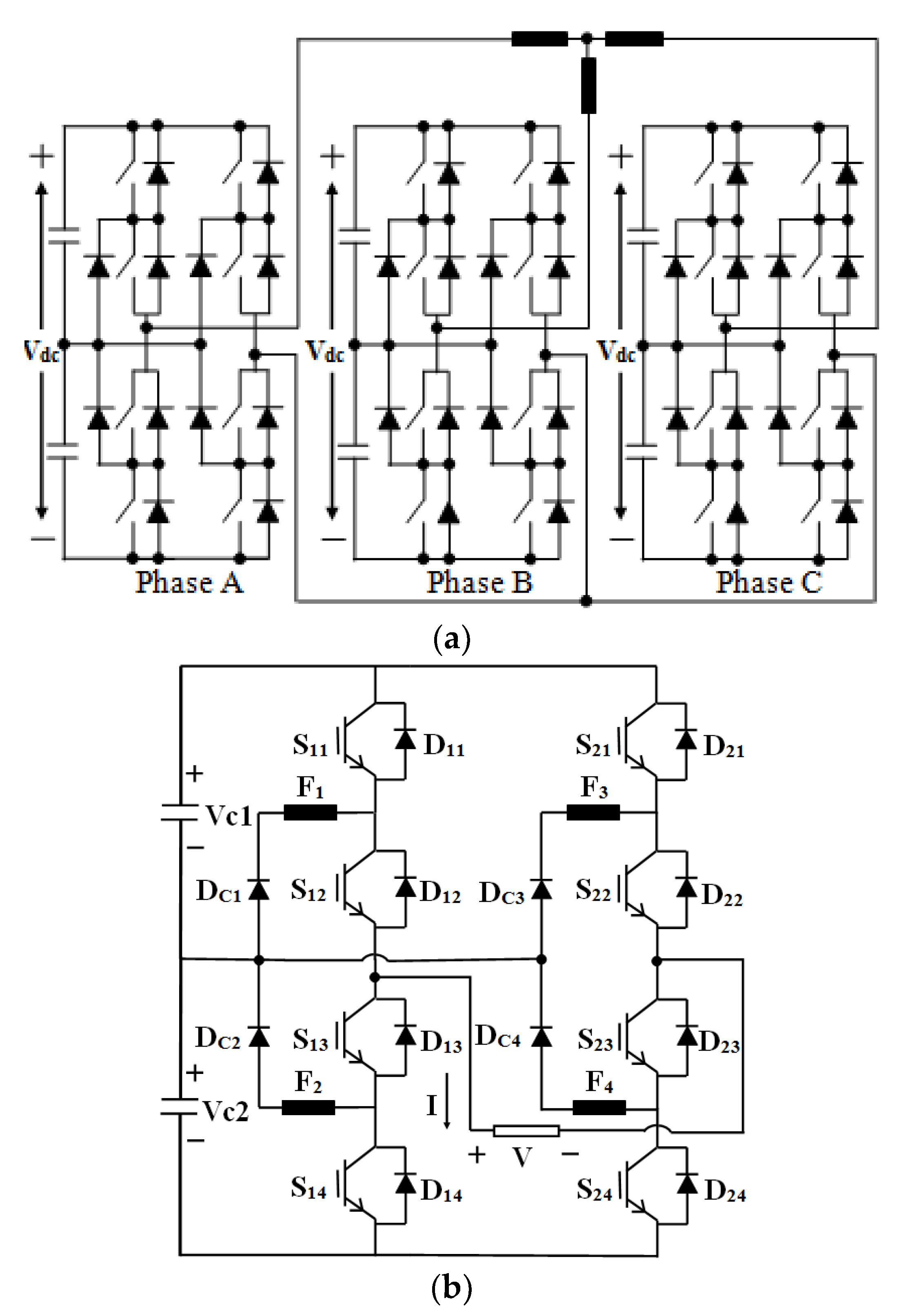
2. Operation of the Inverter under Short-Circuit Fault Condition

Since no redundant component is connected between the phases of the three-phase inverter illustrated in Figure 1a, a fault-tolerant study can be carried out for a single-phase module including fuses for fault-tolerant purposes, as illustrated in Figure 1b. The switching states associated with the corresponding switching patterns are summarized in Table 1. In a healthy condition, the components conducting the load current corresponding to each switching state for positive and negative load currents are indicated in Table 2. As mentioned earlier, the first step to be taken to realize service continuity is eliminating the consequences arising from a short-circuit fault event in a power switch. Short-circuit fault occurrence in a power switch can lead to a short circuit in a DC link capacitor. In this research work, fast fuses are employed to prevent short-circuit occurrence in DC link capacitors. The cost of the fuses compared to that of the other components of the inverter is negligible. In order to locate the fuses in the converter, two matters should be taken into account. Firstly, in the case of a short-circuit fault event in any switch, the DC link capacitors should be protected for all switching states.
Secondly, in the case of blowing a fuse, all voltage levels at the terminal should be achievable during post-fault operation. The fuse cannot be connected in series with S11, S12, S23, or S24 because if the fuse blows, at least the voltage level +Vdc is no longer achievable at the terminal (see Table 2, conducting components corresponding to state 1). In addition, the fuse cannot be connected in series with S21, S21, S13, or S14 because, in these cases, at least the voltage level–Vdc is no longer attainable (see Table 2, conducting components corresponding to state 9). Furthermore, the fuses cannot be connected in series with the DC link capacitors since in the case of a flowing short-circuit current through the fuse and blowing the fuse, the DC link capacitor cannot be served to form the terminal voltage. In this research work, as can be seen in Figure 1b, fuses F1, F2, F3, and F4 are connected in series with clamping diodes DC1, DC2, DC3, and DC4, respectively. In the rest of this section, the role of the fuses to protect the DC link capacitors from a short circuit is investigated and verified. In the next section, the appropriate remedial operation to acquire service continuity is also presented.
Since the presented topology is symmetric, only the left leg is investigated in this section. First of all, it should be noted that, according to Table 1, in switching states 1, 2, and 4, S11 and S12 are switched on; in switching states 3, 5, and 7, switches S12 and S13 are switched on; and in switching states 6, 8, and 9, switches S13 and S14 are switched on. Hence, from the view point of the left leg, the switching states fall into three sets. In the first one, switch pairs (S11, S12) are switched on; in the second one, switch pairs (S12, S13) are switched on; and in the third one, switch pairs (S13, S14) are switched on. In this paper, the first, second, and third set of the switching states are denoted by P, O, and N, respectively. It should be noted that, when a switch encounters to a short-circuit fault, the fault is not eliminated but also the fault consequence is eliminated. In other words, even if the fuse blows, the defected switch remains on short circuit.
In the case of a short-circuit fault occurrence in S11, switching states P and N are applicable to the left leg because, in these switching states, none of the DC link capacitors (neither lower one nor upper one) are short-circuited. Furthermore, in accordance with Table 2, the short-circuit fault in S11 does not hinder the current path in switching states P either for positive or for negative currents. Furthermore, for switching states N, in accordance with Table 2, the short-circuit fault in S11 has no impact on the current path and consequently on the terminal voltage. When switching states, O are applied while S11 is on a short circuit, a clamping diode DC2 is forward-biased, and, as shown in Figure 2a, a current looped is formed by S11, S12, S13, DC2, and the upper DC link capacitor. Thus, the upper DC link capacitor is short-circuited once switching states O are applied and, as a consequence, fuse F2 blows. After blowing fuse F2, applying switching states O do not short-circuit any DC link capacitor.
In the case of a short-circuit fault event in S12, applying switching states P and O do not short-circuit the DC link capacitors because, when the switching states P and O are applied, two clamping diodes, i.e., DC1 and DC2, are reversed biased. When switching states N are applied, clamping diode DC1 is forward biased. Hence, the lower DC link capacitor is short-circuited through DC1, S12, S13, and S14, as illustrated in Figure 2b. Once the short-circuit current flows, fuse F1 blows. Thus, after blowing fuse F1, switching states N can be applied.
In the case of a fault occurrence in S13, switching states N and O can be applied without short-circuiting any DC link capacitor because clamping diodes DC1 and DC2 are reverse biased. When switching states P are applied, clamping diode DC2 is forward-biased. Consequently, the upper DC link capacitor is short-circuited through S11, S12, S13, and DC2 and, as shown in Figure 2c, fuse F2 blows. After blowing fuse F2, switching states P, O, and N can be applied.
When S14 encounters a short-circuit fault, switching states O short-circuit the lower DC link capacitor. As seen in Figure 2d, in this case, the short-circuit current flows through DC1, S12, S13, S14, and the lower DC link capacitor which blows fuse F1. After blowing F1, all switching states can be applied. It should be reminded that, after blowing a fuse, all switching states can be applied without any restriction.
Likewise, all analysis presented for a short-circuit fault event in S11, S12, S13, and S14 can be applied to that in S21, S22, S23, and S24. The presented analysis and explications are summarized in Table 3.
The protection of IGBTs by very fast-acting fuses has already been investigated and validated experimentally in several research works. The research works presented in [32,33,34] propose a short-circuit protection method of power IGBTs by inserting the fast fuses in various places in a power electronic inverter and validate them experimentally. In [33,34], the authors present the consequence arising from the added inductance by standard high-speed fuses. In [34], in order to improve the protection procedure and suppress the consequence of fuse rupture, they investigate the IGBT protection by Tpower fuses instead of standard high speed fuses. In the latter case study, it can be observed that the resulted inductance in the short-circuit current path is lower than those resulted in the former case. The authors in [35] determine the fast fuse rated values according to the switching frequency and characteristics of a power IGBT.
One of the advantages offered by multilevel inverters compared with two-level conventional inverters is the possibility to reduce the switching frequency. Thus, the proposed strategy would be more appropriate for multilevel inverters compared with two level conventional inverters because, as the switching frequency decreases, the practical problem for an IGBT protection decreases.

3. Principle of the Proposed Remedial Strategy

As mentioned earlier, to ensure service continuity in the case of a short-circuit fault event in a power switch, two major steps should be carried out. In the previous section, the first step was elaborated in which the consequences arising from a short-circuit fault event in a power switch is eliminated. In accordance with the studies summarized in Table 3, a short-circuit fault event in each power switch blows a fuse. As a fuse is connected in series with a clamping diode, it can be deduced that blowing a fuse is equivalent to an open-circuit fault occurrence in the clamping diode connected in series with the blown fuse. Thus, the remedial strategy should be presented in the case of an open-circuit fault event in each clamping diode.
It should be mentioned that, for realization of the proposed strategy, short-circuit fault identification is not required. Corresponding to a short-circuit fault event in an IGBT, a specific fuse blows. After blowing the fuse, the destructive consequence of the short-circuit fault (short-circuiting the DC link capacitors) is prevented. Therefore, after blowing the fuse, all of switching states can be applied without forming any short-circuit current loop. The fuse blows when certain switching states are applied (see Table 3). Hence, it can be concluded that blowing a fuse does not require any short-circuit fault identification.
Blowing the fuse can be treated as an open-circuit fault in the clamping diode connected in series with the melted fuse. Hereafter, the open-clamping diode (or blown fuse) has to be identified in order to apply the relevant remedial control (see Table 4).
In summary, the short-circuited IGBT is not identified but also the blown fuse (the open-circuited clamping diode) is identified which is prerequisite to applying the relevant remedial control approach. The short-circuited IGBT remains on a short circuit but it does not lead to any restriction or harmful consequence.

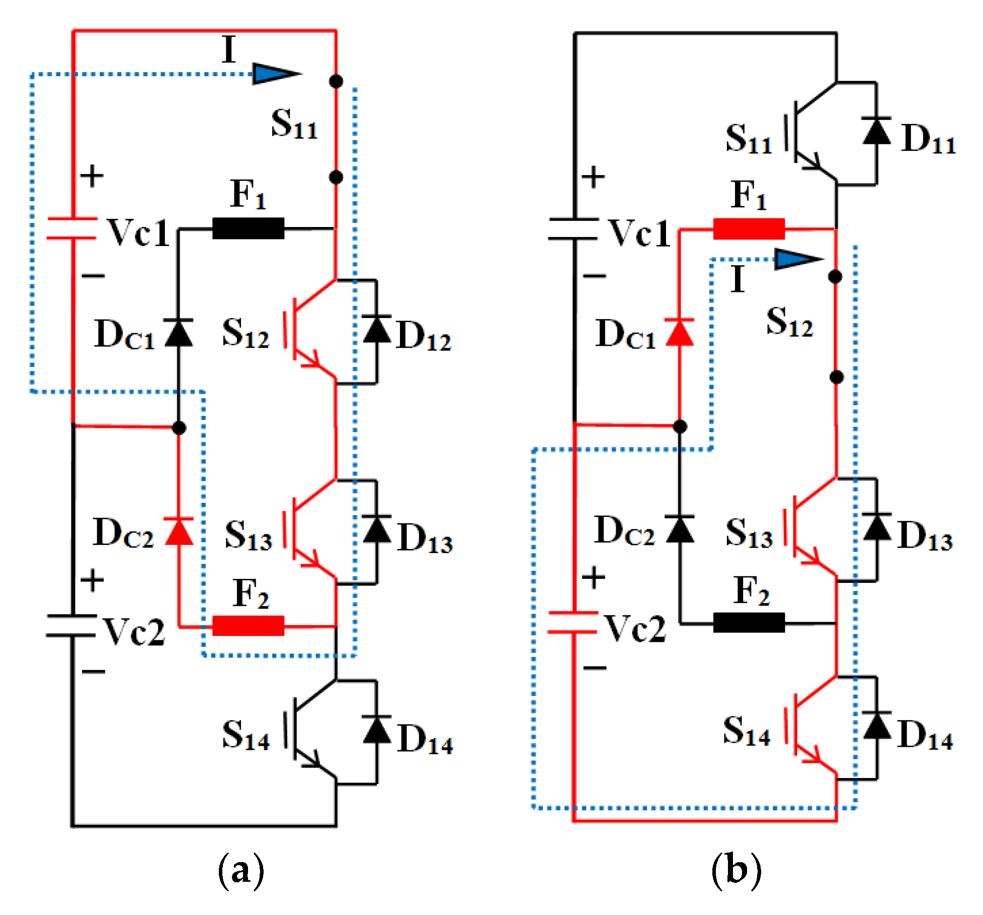
3.1. Remedial Strategy in the Case of Blowing Fuse F1 or Fuse F2

As mentioned above, blowing fuse F1 or F2 can be considered as an open-circuit fault event in clamping diode DC1 or DC2, respectively. According to Table 3, a short-circuit fault event in S12 or S14 leads to blow fuse F1 (open-circuit fault in DC1) and short-circuit fault occurrence in S11 or S13 results in blowing fuse F2 (an open-circuit fault event in DC2). As can be seen in Table 2, in switching states 3, 5, and 7, clamping diodes DC1 (while the terminal current is positive) and DC2 (while the terminal current is negative) form the current path. Hence, in the case of an open-circuit fault event in DC1 or DC2 (blowing F1 or F2), by applying switching states 3, 5, and 7, the desired terminal voltages are no longer achievable. To solve this matter, these infeasible switching states are substituted with other switching states with which the desired terminal voltages are attainable. According to Table 2, by applying switching states 2 and 3, the same terminal voltage (+Vdc/2) is acquired while, by applying switching state 2, the terminal current flows neither through DC1 nor through DC2 either for positive or negative currents. Thus, infeasible switching state 3 is replaced by switching state 2. Furthermore, applying switching states 4, 5, or 6, results in the same terminal voltage (0 V). Hence, instead of applying switching state 5, switching state 4 or 6 can be applied in which neither DC1 nor DC2 form the terminal current path. It should be noted that both switching states 4 and 6 have the same impact on the DC link capacitors’ voltages and, consequently, on the neutral point voltage. According to Table 2, while switching state 4 or 6 is applied, either for positive current or for negative terminal currents, no current is injected to the neutral point. Likewise, it can be concluded that infeasible switching state 7 (corresponding to –Vdc/2 at the terminal) is replaced by switching state 8. The analysis presented in this subsection is summarized in Table 4.

3.2. Remedial Strategy in the Case of Blowing Fuse F3 or Fuse F4

Similar to the analysis presented in the previous subsection, blowing fuse F3 or F4 can be interpreted as an open-circuit fault occurrence in clamping diode DC3 or DC4, respectively. In accordance with Table 2, while switching states 2, 5, and 8 are applied in healthy condition, clamping diodes DC3 (for positive terminal currents) and DC4 (for negative terminal currents) contribute to form the terminal current path. Hence, in the case of an open-circuit fault event in DC3 (blowing F3) or in DC4 (blowing F4), switching states 2, 5, and 8 are infeasible.
By applying the similar analysis presented in the previous subsection, it can be deduced that the switching states 2, 5, and 8 should be substituted with switching states 3, 4 or 6, and 7, respectively. The analysis presented in this subsection is also summarized in Table 4.

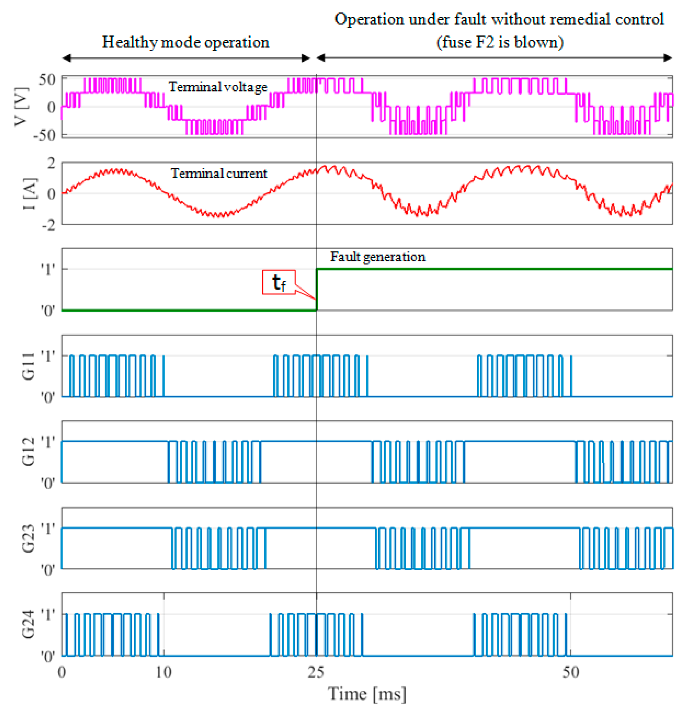
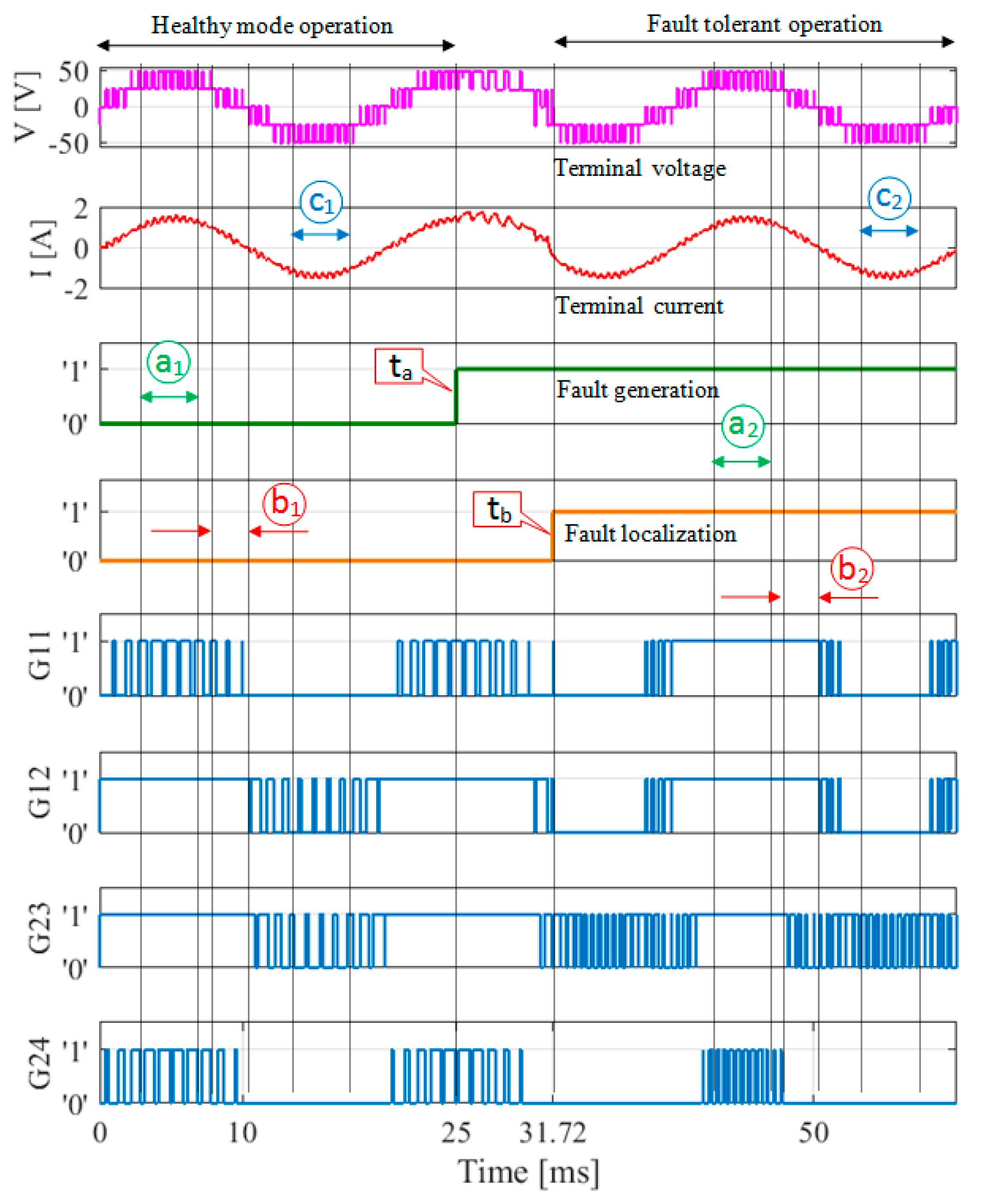
4. Simulation Results

The simulation results are presented in two subsections. In the first one, the simulation results regarding a short-circuit fault-tolerant approach applied to switches S11, S12, S13, or S14 (fuse F1 or fuse F2 blows) are provided and discussed. In the second subsection, fault-tolerant operation of the inverter in the case of a short-circuit fault event in switches S21, S22, S23, and S24 (fuse F3 or fuse F4 blows) are represented.
The simulation parameters associated with their values are provided in Table 5. The inverter feeds a resistive-inductive load.
It should be mentioned that the fault-tolerant operation of the inverter begins once the blown fuse (resulting in an open-circuit fault in the clamping diode) is detected.
In other words, prior to applying remedial control, localization of the open-circuit fault in the clamping diode is necessary. Since this research work only deals with fault-tolerant operation and solely targets the remedial actions to ensure service continuity of the inverter, the fault localization step is not addressed in this paper. Open-circuit fault localization for clamping diodes in an NPC inverter presented in research works [18,36,37] can be applied. The simulations are carried out in MATLAB/Simulink environment.

4.1. Simulation Results Regarding Service Continuity in the Case of Blowing Fuse F1 or Fuse F2

As presented in Table 3, short-circuit fault occurrence in switches S11, S12, S13, or S14 leads to blow fuse F1 or F2. In addition, in accordance with the analysis summarized in Table 4, it can be observed that, in the case of blowing F1 or F2, the same remedial control is applied to ensure service continuity of the inverter because the infeasible and substituted switching states corresponding to these two cases are same. It is worth reminding that blowing fuse F1 or F2 are considered as an open-circuit fault event in DC1 or DC2, respectively.
As can be observed in Table 1, the gate signals corresponding to switches S11, S12, S23, and S24 are complementary to those corresponding to switches S13, S14, S21, and S22, respectively. In this regard, in the simulation results only the gate signals applied to switches S11, S12, S23, and S24 are presented and denoted by G11, G12, G23, and G24, respectively.
Before presenting the applied remedial control, the operation of inverter under short-circuit fault occurrence without applying remedial control is represented. For this purpose, and in order to avoid presenting similar and repetitive results, solely the results regarding the inverter operation under a short-circuit fault event in switch S11 are selected and presented in Figure 3. As can be seen in Figure 3, before a short-circuit fault event at instant tf, the inverter operates in healthy operation. During post-fault operation, fuse F2 is blown (equivalent to an open-circuit fault in clamping diode DC2). As mentioned earlier, the fuses connected in series with the clamping diodes protect the DC link capacitors in the case of a short-circuit fault event. Subsequent to blowing a fuse which leads to an open-circuit fault in a clamping diode, the terminal voltage and current of the inverter are distorted compared to the healthy operation. Thus, by applying a remedial control during post-fault operation, the terminal voltage and current obtained during healthy operation would be restored.
In order to represent the applied remedial approach, the inverter operation during healthy condition is compared with the post-fault operation of the inverter. In this regard, the switching states applied during healthy operation are compared with those applied during post-fault operation. Figure 4 represents the simulation results regarding fault-tolerant operation of the inverter in the case of a short-circuit fault event in switch S11. Before instant ta, the inverter operates in healthy condition. At instant ta, a short-circuit fault occurs in S11. As explained earlier, according to Table 3, in the case of a short-circuit fault event in S11, once one of switching states 3, 5, or 7 is applied, fuse F2 blows (equivalent to an open-circuit fault in DC2). According to Figure 4, at instant tb, the blown fuse (faulty clamping diode) is identified and, subsequent to the fault identification, the remedial control is applied to ensure the service continuity. As seen in Figure 4, during fault-tolerant operation, the rated voltage and current are acquired, and the terminal current and voltage are not distorted compared to those during healthy operation.
In order to investigate the applied remedial operation in Figure 4, intervals a1, b1, and c1 (healthy operation) are compared to intervals a2, b2, and c2 (fault-tolerant operation), respectively. During interval a1, gate signals of S12 and S23 (G12 and G23) are set at ‘1′ and gate signals of S11 and S24 (G11 and G24) toggle between ‘1′ and ‘0′. In accordance with Table 1, it can be concluded that, during interval a1, switching states 1, 2, and 3 are applied to the power switches. As seen in Figure 4, during interval a2, the same voltage levels are obtained compared to interval a1 while, during interval a2, gate signals of S11 (G11), S12 (G12), and S23 (G23) are set at ‘1′ and gate signal of S24 (G24) toggles between ‘1′ and ‘0′. Hence, in accordance with Table 1, it can be deduced that only switching states 1 and 2 are applied. Thus, by comparing the switching states applied in interval a1 to those applied during interval a2, it can be observed that, during fault-tolerant operation in the case of a fault in S11 (F2 blows according to Table 4), switching state 3 is no longer applied during fault-tolerant operation and this infeasible switching state is replaced by switching state 2 which complies with the analysis presented in Table 4 (the subsection corresponding to F2). During interval b1, gate signals of S12 (G12) and S23 (G23) are set at ‘1′ and gate signals of S11 (G11) and S24 (G24) toggle between ‘0′ and ‘1′. Thus, according to Table 1, switching states 2, 3, and 5 are applied to the power switches. Over entire interval b2, signals G11 and G12 are set at ‘1′, G24 is set at ‘0′, and signal G23 toggles between ‘1′ and ‘0′. Referring to Table 1, it can be observed that, during interval b2, switching states 2 and 4 are applied. Thus, by comparing the switching states applied during intervals b1 and b2, it is deduced that the infeasible switching states 3 and 5 are substituted with switching states 2 and 4 which complies with the analysis provided in Table 4 (the subsection corresponding to fuse F2). As mentioned previously, infeasible switching state 5 can be replaced either by switching state 4 or 6 (here, switching state 4 is chosen). Likewise, by observing the switching states applied during intervals c1 and c2 in Figure 4, it is deduced that, during interval c1, switching states 7, 8, and 9 are applied while, during post-fault operation (interval c2), switching states 8 and 9 are applied. Thus, infeasible switching state 7 is substituted with switching state. The similar analysis applied to Figure 4 can also be applied to Figure 5, Figure 6 and Figure 7, which illustrate fault-tolerant operation of the inverter in the case of a short-circuit fault event in switches S12, S13, and S14, respectively. It should be reminded that, according to Table 3, a short-circuit fault event in S12, S13, or S14 blows fuses F1, F2, or F1, respectively. On the other hand, according to Table 4, in the case of a blowing fuse F1 or F2, the same remedial strategy is carried out to ensure service continuity. The presented analysis consisting of the applied switching states during the healthy operation and post-fault operation of the inverter in the case of a short-circuit fault in S11, S12, S13, and S14 are summarized in Table 6.
It should be noted that the length of the intervals located between the fault generation instant and the beginning of the remedial control (interval [ta, tb]), in the results presented in Figure 4, Figure 5, Figure 6 and Figure 7, are not equal. As explained previously, these intervals correspond to the open-circuit fault localization time of the clamping diodes which is not targeted in this research work. In the following, this matter is clarified.
In the case of a short-circuit fault event in S11, fuse F2 blows (resulting in an open-circuit fault in clamping diode DC2). From one hand, according to Figure 4, a short-circuit fault occurs (instant ta) when the terminal current is positive. On the other hand, clamping diode DC2 conducts only when the terminal current is negative (see Table 2). Thus, as long as the terminal current is positive (during interval [ta, tb]), the clamping diode DC2 does not have any contribution to make the terminal current and voltage. Thus, during this interval, the fault localization cannot be accomplished and, consequently, applying the remedial control does not begin. This interval (localization time) should elapse and it is not avoidable. The similar analysis can be applied to the three other cases.

4.2. Simulation Results Regarding Service Continuity in the Case of Blowing Fuse F3 or Fuse F4

By referring to Table 3, it is observed that short-circuit fault occurrence in S21, S22, S23, or S24 blows fuse F3 or F4. Thus, this subsection deals with a fault-tolerant operation study of the inverter in the case of a short-circuit fault event in S21, S22, S23, or S24. In addition, according to the analysis summarized in Table 4, in the case of blowing fuse F3 (equivalent to an open-circuit fault event in DC3) or fuse F4 (equivalent to an open-circuit fault event in DC4), the same remedial strategy is applied during fault-tolerant operation. In other words, the same remedial strategy is applied in the case of a fault event in S21, S22, S23, and S24. In this subsection, the simulation results regarding fault-tolerant operation of the inverter in the case of a short-circuit fault in switch S21, S22, S23, or S24 are depicted in Figure 8, Figure 9, Figure 10 and Figure 11, respectively.
As can be seen in Figure 8, Figure 9, Figure 10 and Figure 11, the acquired terminal current and voltage waveforms during post-fault operation are similar to those obtained during healthy operation. Similar to the previous subsection, in order to elaborate the employed remedial control, the applied switching states during three intervals a1, b1, and c1 are compared to those applied during three intervals a2, b2, and c2, respectively. To avoid verbosity, the comparison results are provided in Table 7. As can be observed in Table 7, infeasible switching states 2, 5, and 8 are substituted by switching states 3, 4, and 7.

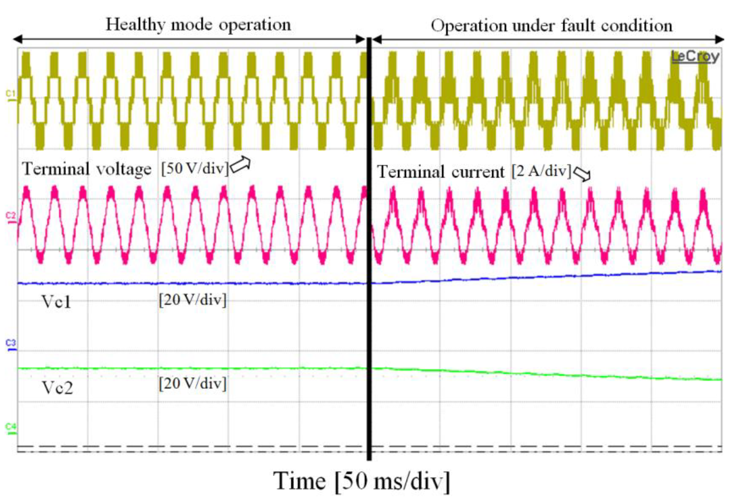
5. Experimental Results

The NPC inverter is constituted of IGBTs SKM50GB123D of SEMIKRON (SEMIKRON, Nuremberg, Germany), commanded by SKHI22A drivers (SEMIKRON, Nuremberg, Germany). For the experimental setup, the load resistance, the load inductance, the switching frequency, the fundamental frequency, the DC link capacitors, the DC link voltage, and modulation index are set at 27.7 Ω, 9 mH, 1 kHz, 50 Hz, 2.2 mF, 50 V, and 0.8, respectively. The modulation part is implemented on a real-time processor of a MicroLabBox (dSpace® platform) (SEMIKRON, Nuremberg, Germany), and the fault diagnosis and the fault-tolerant control subsections are implemented on the FPGA chip of the MicroLabBox (Xilinx® Kintex®-7 XC7K325T). The clock frequency of the FPGA chip is set at 100 MHz. In the experimental results, the switching pattern is illustrated by four selected IGBTs gate signals. Based on these four IGBTs gate signals, the switching state can be determined according to Table II because the command signals corresponding to the other four IGBTs are complementary. The experimental setup is represented in Figure 12.
The proposed short-circuit fault-tolerant strategy does not require any additional component. As mentioned earlier, a short-circuit fault in a switch or in a diode leads to blow in a fuse which is treated as an open-circuit fault in a clamping diode. Solely by modifying the infeasible switching states applied in healthy operation, the fault-tolerant operation is realized. Figure 13 represents the inverter operation in the case of a short-circuit fault in S21 (blowing fuse F4) without applying fault-tolerant strategy. As can be seen, once the fault occurs (after blowing fuse F4), the two DC link capacitors’ voltages start to diverge from their rated values in such a way that one of them attains entire DC link voltage and the other one would be discharged completely. Thus, one of the capacitors would be exposed to overvoltage. Furthermore, after the fault event, the output voltage and current are deteriorated in terms of distortion. The outcomes of the applied fault-tolerant strategy (in the case of blowing F4) are illustrated in Figure 14 and Figure 15. As shown in Figure 14, by applying the fault-tolerant strategy, the output voltage and current obtained during fault-tolerant operation are identical to those obtained during healthy operation.
Moreover, despite low-frequency oscillation with negligible ripple amplitude in the DC link capacitors’ voltages, the middle-point voltage of a DC bus is stabilized. In Figure 15, by comparing the healthy operation with the fault-tolerant operation of the inverter (in the case of blowing F4), the modifications of the switching states are represented. In this regard, the switching states corresponding to the same voltage levels (healthy operation and fault-tolerant operation) obtained at the output are compared. It should be reminded that blowing fuse F4 can be treated as an open-circuit fault event in DC4. In Figure 15, four gate signals comprising G11 (gate signal of S11), G12 (gate signal of S12), G23 (gate signal of S23), and G24 (gate signal of S24) are selected to represent the applied switching states. Gate signals applied to S13, S14, S21, and S22 are complementary to those corresponding to S11, S12, S23, and S24, respectively (see Table 1). Thus, from the four mentioned gate signals, the corresponding switching state is determined. In interval a1, the voltage levels made at the output in healthy mode are +Vdc and +Vdc/2. According to the gate signals and Table 1, switching states 1, 2, and 3 are applied in this interval. In interval a2, the same output voltage levels are obtained compared with interval a1 but the switching state 2 is substituted with switching state 3. Indeed, over entire interval a2, G12, G23, and G24 are set at ‘1′ and solely G11 is toggled between ‘0′ and ‘1′ which complies with Table 7, according to the switching patterns provided in Table 1 for switching states 1, 2, and 3. In interval b1, the output voltage levels −Vdc and −Vdc/2 are achieved. Based on the represented gate signals in interval b1 and Table 1, switching states 7, 8, and 9 are applied in this interval. By performing a detailed comparison between the gate signals applied in interval b2 (fault-tolerant operation) with those applied in interval b1, one can deduce that switching state 8 is replaced by switching state 7 (G11, G23, and G24 are set at ‘0′ and G12 is toggled between ‘0′ and ‘1′) which conforms to the data provided in Table 7. Likewise, by comparison of interval c1 with interval c2, it is deduced that, during fault-tolerant operation, switching states 2 and 5 are substituted with switching states 3 and 4, respectively.

6. Conclusions

In this paper, a short-circuit fault-tolerant five-level NPC/H-Bridge inverter associated with the remedial strategy is presented. The proposed fault-tolerant strategy consists of two major parts. In the first part, by connecting the fuses in series with the clamping diodes, two paramount purposes are achieved. Firstly, the DC link capacitors are protected. Secondly, in the case of blowing a fuse, all voltage levels are still achievable at the terminal by applying remedial control. In the second part, by applying the proposed remedial control, the rated terminal voltage and current are obtained during fault-tolerant operation. Furthermore, the harmonic content of the terminal voltage and current is not deteriorated compared to the healthy operation. The remedial control is realized by modifying the switching states which does not require any redundant component. Only four fast fuses are connected in series with the clamping diodes whose cost, compared with the other components of the inverter, is negligible. The proposed fault-tolerant strategy has been solely examined and experimentally validated for a NPC/H-bridge structure. However, the general concept of the proposed method could be developed for the other structures, such as T-type, A-NPC, and flying capacitor.

Author Contributions

Investigation: S.A., P.P. and S.S.; Methodology: S.A., P.P. and S.S.; Supervision: P.P., S.S. and D.A.K.; Writing—original draft: S.A.; Writing—review & editing: P.P., D.A.K. and S.S. All authors have read and agreed to the published version of the manuscript.

Funding

This research work is the result of the collaboration between University of Lorraine (France) and Iran University of Science and Technology (IUST) started in October 2017. It has been partially financially supported by the Scientific and Technologique Cooperation Service of French Embassy in Tehran that we would like to thank.

Conflicts of Interest

The authors declare no conflict of interest.

References

  1. Gautam, S.P.; Kumar, L.; Gupta, S.; Agrawal, N. A single-phase five-level inverter topology with switch fault-tolerance capabilities. IEEE Trans. Ind. Electron. 2017, 64, 2004–2014. [Google Scholar] [CrossRef]
  2. Rodriguez, J.; Lai, J.S.; Peng, F.Z. Multilevel inverters: A survey of topologies, controls, and applications. IEEE Trans. Ind. Electron. 2002, 49, 724–738. [Google Scholar] [CrossRef] [Green Version]
  3. Jung, J.; Ku, H.; Son, Y.; Kim, J. Open-switch fault diagnosis algorithm and tolerant control method of the three-phase three-level NPC active rectifier. Energies 2019, 12, 2495. [Google Scholar] [CrossRef] [Green Version]
  4. Wu, B. High-Power Converters AC Drives; Wiley: Hoboken, NJ, USA, 2006. [Google Scholar]
  5. Baek, S.; Shin, H.; Kang, S.; Park, C.; Lee, K. Open fault detection and tolerant control for a five phase inverter driving system. Energies 2016, 9, 335. [Google Scholar] [CrossRef] [Green Version]
  6. Lezana, P.; Pou, J.; Meynard, T.; Rodríguez, J.; Ceballos, S.; Richardeau, F. Survey on fault operation on multilevel inverters. IEEE Trans. Ind. Electron. 2010, 57, 2207–2218. [Google Scholar] [CrossRef] [Green Version]
  7. Blinov, A.; Kosenko, R.; Chub, A.; Ivakhno, V. Analysis of fault-tolerant operation capabilities of an isolated bidirectional current-source DC-DC converter. Energies 2019, 12, 3203. [Google Scholar] [CrossRef] [Green Version]
  8. Lamb, J.; Mirafzal, B. Open-circuit IGBT fault detection and location isolation for cascaded multilevel converters. IEEE Trans. Ind. Electron. 2017, 64, 4846–4856. [Google Scholar] [CrossRef]
  9. Ouni, S.; Zolgadri, M.R.; Khodabandeh, M.; Shahbazi, M.; Rodriguez, J.; Oraee, H.; Lezana, P.; Schmeisser, A.U. Improvement of post-fault performance of a cascaded H-bridge multilevel inverter. IEEE Trans. Ind. Electron. 2017, 64, 2779–2788. [Google Scholar] [CrossRef] [Green Version]
  10. Salimian, H.; Iman-Eini, H. Fault-tolerant operation of three-phase cascaded H-bridge converters using an auxiliary module. IEEE Trans. Ind. Electron. 2017, 64, 1018–1027. [Google Scholar] [CrossRef]
  11. Aleenejad, M.; Mahmoudi, H.; Moamaei, P.; Ahmadi, R. A new fault-tolerant strategy based on a modifies selective harmonic technique for three-phase multilevel converters with a single faulty cell. IEEE Trans. Power Electron. 2016, 31, 3141–3150. [Google Scholar] [CrossRef]
  12. Abdelsalam, M.; Marei, M.I.; Tennakoon, S.B. An integrated control strategy with fault detection and tolerant control capability based on capacitor voltage estimation for modular multilevel converters. IEEE Trans. Ind. Appl. 2017, 53, 2840–2851. [Google Scholar] [CrossRef]
  13. Ghazanfari, A.; Mohamed, Y.A.I. A resilient framework for fault-tolerant operation of modular multilevel converters. IEEE Trans. Ind. Electron. 2016, 63, 2669–2678. [Google Scholar] [CrossRef]
  14. Li, B.; Shi, S.; Wang, B.; Wang, G.; Wang, W.; Xu, D. Fault diagnosis and tolerant control of single IGBT open-circuit failure in modular multilevel converters. IEEE Trans. Power Electron. 2016, 31, 3165–3176. [Google Scholar] [CrossRef]
  15. Deng, F.; Tian, Y.; Zhu, R.; Chen, Z. Fault-tolerant approach for modular multilevel converters under submodule faults. IEEE Trans. Ind. Electron. 2016, 63, 7253–7263. [Google Scholar] [CrossRef]
  16. Yang, S.; Tang, Y.; Wang, P. Seamless fault-tolerant operation of a modular multilevel converter with switch open-circuit fault diagnosis in a distributed control architecture. IEEE Trans. Power Electron. 2017, 33, 7058–7070. [Google Scholar] [CrossRef]
  17. Lee, J.S.; Lee, K. Open-switch fault tolerance control for a three-level NPC/T-type rectifier in wind turbine systems. IEEE Trans. Ind. Electron. 2015, 62, 1012–1021. [Google Scholar] [CrossRef]
  18. Choi, U.; Lee, J.; Blaabjerg, F.; Lee, K. Open-circuit fault diagnosis and fault-tolerant control for a grid-connected NPC inverter. IEEE Trans. Power Electron. 2016, 31, 7234–7247. [Google Scholar] [CrossRef]
  19. Ceballos, S.; Pou, J.; Zaragoza, J.; Robles, E.; Villate, J.L.; Martín, J.L. Fault-tolerant neutral-point-clamped converter solutions based on including a fourth resonant leg. IEEE Trans. Ind. Electron. 2011, 58, 2293–2303. [Google Scholar] [CrossRef]
  20. Li, S.; Xu, L. Strategies of fault tolerant operation for three-level PWM inverters. IEEE Trans. Ind. Electron. 2006, 21, 933–940. [Google Scholar] [CrossRef]
  21. Ceballos, S.; Pou, J.; Robles, E.; Gabiola, I.; Zaragoza, J.; Villate, J.L.; Boroyevich, D. Three-level converter topologies with switch breakdown fault-tolerance capability. IEEE Trans. Ind. Electron. 2008, 55, 982–995. [Google Scholar] [CrossRef]
  22. Ceballos, S.; Pou, J.; Robles, E.; Zaragoza, J.; Martín, J.L. Performance evaluation of fault-tolerant neutral-point-clamped converters. IEEE Trans. Ind. Electron. 2010, 57, 2709–2718. [Google Scholar] [CrossRef]
  23. Lee, J.; Lee, K. Open-circuit fault-tolerant control for outer switches of three-level rectifiers in wind turbine systems. IEEE Trans. Power Electron. 2016, 31, 3806–3815. [Google Scholar] [CrossRef]
  24. Katebi, R.; He, J.; Weise, N. An advanced three-level active neutral-point-clamped converter with improved fault-tolerant capabilities. IEEE Trans. Power Electron. 2018, 33, 6897–6909. [Google Scholar] [CrossRef] [Green Version]
  25. Azer, P.; Ouni, S.; Narimani, M. A novel fault-tolerant technique for active neutral point clamped inverter using carrier-based PWM. IEEE Trans. Ind. Electron. 2020, 67, 1792–1803. [Google Scholar] [CrossRef]
  26. Xu, S.; Zhang, J.; Hang, J. Investigation of a fault-tolerant three-level T-type inverter system. IEEE Trans. Ind. Appl. 2017, 53, 4613–4623. [Google Scholar] [CrossRef]
  27. Choi, U.M.; Blaabjerg, F.; Lee, K.B. Reliability improvement of a T-type three-level inverter with fault-tolerant control strategy. IEEE Trans. Power Electron. 2015, 30, 2660–2673. [Google Scholar] [CrossRef]
  28. Choi, U.; Lee, K.; Blaabjerg, F. Diagnosis and tolerant strategy of an open-switch fault for T-type three-level inverter systems. IEEE Trans. Ind. Appl. 2014, 50, 495–508. [Google Scholar] [CrossRef]
  29. Lee, T.; Li, B.; Yang, M.; Tsai, Y. A Carrier-Based PWM for Three-Level T-Type Inverter to Tolerate Open-Circuit Fault. IEEE Trans. Power Electron. 2018, 33, 8787–8796. [Google Scholar] [CrossRef]
  30. He, J.; Katebi, R.; Weise, N.; Demerdash, N.A.O.; Wei, L. A fault-tolerant T-type multilevel inverter topology with increased overload capability and soft-switching characteristics. IEEE Trans. Ind. Appl. 2017, 53, 2826–2839. [Google Scholar] [CrossRef]
  31. Li, J. Design and Control Optimisation of A Novel Bypass-Embedded Multilevel Multicell Inverter for Hybrid Electric Vehicle Drives. In Proceedings of the 2020 IEEE 11th International Symposium on Power Electronics for Distributed Generation Systems (PEDG), Dubrovnik, Croatia, 28 September–1 October 2020; pp. 382–385. [Google Scholar]
  32. Braun, G.; Pixler, D.; Lemay, P. IGBT Module Rupture Categorization and Testing. In Proceedings of the IEEE Industry Application Socity Annual Meeting, New Orleans, LA, USA, 5–9 October 1997. [Google Scholar]
  33. Blaabjerg, F.; Iov, F.; Ries, K. Fuse protection of IGBT modules against explosions. J. Power Electron. 2002, 2, 88–94. [Google Scholar]
  34. Iov, F.; Abrahamsen, F.; Blaabjerg, F.; Ries, K.; Rasmussen, H.; Bjornaa, P. Fusing IGBT Based Inverters. In Proceedings of the PCIM 2001: International Conference on Power Electronics, Intelligent Motion and Power Quality, Nurenberg, Germany, 19–21 June 2001. [Google Scholar]
  35. Duong, S.; Schaeffer, C.; Rouve, L.; Palma, J.; Mullert, C. Fuses for Power IGBT Converters. In Proceedings of the IEEE Industry Applications Society Annual Meeting, Denver, CO, USA, 2–6 October 1994. [Google Scholar]
  36. Mendes, A.M.S.; Abadi, M.B.; Cruz, S.M.A. Method to diagnose open-circuit faults in active power switches and clamp-diodes of three-level neutral-point clamped inverters. IET Elect. Power Appl. 2016, 10, 623–632. [Google Scholar]
  37. Ge, X.; Pu, J.; Geo, B.; Liu, Y. An open-circuit fault diagnosis approach for single-phase three-level neutral-point-clamped converters. IEEE Trans. Power. Electron. 2018, 33, 2559–2570. [Google Scholar] [CrossRef]
Figure 1. Scheme of (a) a conventional three-phase five-level NPC/H-bridge inverter; (b) a single-phase five-level NPC inverter with short-circuit fault-tolerant capability (fuses are included).
Electronics 10 02411 g001
Figure 2. Short-circuit current loop in the case of a short-circuit fault event in: (a) S11; (b) S12; (c) S13; (d) S14.
Electronics 10 02411 g002aElectronics 10 02411 g002b
Figure 3. Simulation results for operation of the inverter under a short-circuit fault event in S11 without applying remedial control.
Electronics 10 02411 g003
Figure 4. Simulation results for fault-tolerant operation of the inverter in the case of a short-circuit fault event in S11.
Electronics 10 02411 g004
Figure 5. Simulation results for fault-tolerant operation of the inverter in the case of a short-circuit fault event in S12.
Electronics 10 02411 g005
Figure 6. Simulation results for fault-tolerant operation of the inverter in the case of a short-circuit fault event in S13.
Electronics 10 02411 g006
Figure 7. Simulation results for fault-tolerant operation of the inverter in the case of a short-circuit fault event in S14.
Electronics 10 02411 g007
Figure 8. Simulation results for fault-tolerant operation of the inverter in the case of a short-circuit fault event in S21.
Electronics 10 02411 g008
Figure 9. Simulation results for fault-tolerant operation of the inverter in the case of a short-circuit fault event in S22.
Electronics 10 02411 g009
Figure 10. Simulation results for fault-tolerant operation of the inverter in the case of a short-circuit fault event in S23.
Electronics 10 02411 g010
Figure 11. Simulation results for fault-tolerant operation of the inverter in the case of a short-circuit fault event in S24.
Electronics 10 02411 g011
Figure 12. Experimental setup.
Electronics 10 02411 g012
Figure 13. Experimental results of the inverter operation after blowing fuse F4 without applying fault diagnosis and fault-tolerant control.
Electronics 10 02411 g013
Figure 14. Experimental results of the inverter operation with fault-tolerant control in the case of blowing fuse F4.
Electronics 10 02411 g014
Figure 15. Detailed experimental results of the fault-tolerant strategy in the case of blowing fuse F4.
Electronics 10 02411 g015
Table 1. Switching patterns corresponding to each voltage level.
Switching StateTerminal VoltageS11S12S13S14S21S22S23S24
1 +Vdc 1 1 0 0 0 0 1 1
2 +Vdc/2 1 1 0 0 0 1 1 0
3 +Vdc/2 0 1 1 0 0 0 1 1
4 0 1 1 0 0 1 1 0 0
5 0 0 1 1 0 0 1 1 0
6 0 0 0 1 1 0 0 1 1
7 −Vdc/2 0 1 1 0 1 1 0 0
8 −Vdc/2 0 0 1 1 0 1 1 0
9 −Vdc 0 0 1 1 1 1 0 0
Table 2. Conducting components corresponding to each switching state for positive and negative output currents in healthy operation.
Switching StateTerminal
Voltage
Conducting
Components (I > 0)
Conducting
Components (I < 0)
1+VdcS11, S12, S23, S24D11, D12, D23, D24
2+Vdc/2S11, S12, S23, DC4D11, D12, S22, DC3
3+Vdc/2DC1, S12, S23, S24DC2, S13, D23, D24
40S11, S12, D22, D21D11, D12, S21, S22
50DC1, S12, S23, DC4DC2, S13, S22, DC3
60D14, D13, S23, S24S13, S14, D24, D23
7−Vdc/2DC1, S12, D22, D21DC2, S13, S22, S21
8−Vdc/2D14, D13, S23, DC4S13, S14, DC3, S22
9−VdcD14, D13, D22, D21S13, S14, S22, S21
Table 3. Switching states making short-circuit current loop corresponding to each component.
Faulty ComponentSwitching States (Table 1) Making Short-Circuit Current LoopBlown Fuse
S113, 5, 7F2
S126, 8, 9F1
S131, 2, 4F2
S143, 5, 7F1
S212, 5, 8F4
S221, 3, 6F3
S234, 7, 9F4
S242, 5, 8F3
Table 4. Modification of the infeasible switching states to ensure service continuity.
Blown FuseClamping Diode in Series with the Blown FuseInfeasible Switching StateSubstituted Switching State
F1DC132
54 or 6
78
F2DC232
54 or 6
78
F3DC323
54 or 6
87
F4DC423
54 or 6
87
Table 5. Simulation parameters associated with their values.
ParameterValue
Load resistance27.7 Ω
Load inductance9 mH
DC link voltage50 V
DC link capacitor2.2 mF
Switching frequency1 kHz
Modulation index0.8
Table 6. Applied switching states corresponding to each interval in Figure 4, Figure 5, Figure 6 and Figure 7.
IntervalApplied Switching States
a11, 2, 3
b12, 3, 5
c17, 8, 9
a21, 2
b22, 4
c28, 9
Table 7. Applied switching states corresponding to each interval in Figure 8, Figure 9, Figure 10 and Figure 11.
IntervalApplied Switching States
a11, 2, 3
b12, 3, 5
c17, 8, 9
a21, 3
b23, 4
c27, 9
Publisher’s Note: MDPI stays neutral with regard to jurisdictional claims in published maps and institutional affiliations.

