Abstract
In this study, sol–gel-processed Li-doped SnO2-based thin-film transistors (TFTs) were fabricated on SiO2/p+ Si substrates. The influence of Li dopant (wt%) on the structural, chemical, optical, and electrical characteristics was investigated. By adding 0.5 wt% Li dopant, the oxygen vacancy formation process was successfully suppressed. Its smaller ionic size and strong bonding strength made it possible for Li to work as an oxygen vacancy suppressor. The fabricated TFTs consisting of 0.5 wt% Li-doped SnO2 semiconductor films delivered the field-effect mobility in a 2.0 cm2/Vs saturation regime and Ion/Ioff value of 1 × 10⁸ and showed enhancement mode operation. The decreased oxygen vacancy inside SnO2 TFTs with 0.5 wt% Li dopant improved the negative bias stability of TFTs.
1. Introduction
Recently, the demand for oxide semiconductors has been increased due to their high usability. Oxide semiconductor-based thin-film transistors (TFTs) show higher mobility than amorphous phase Si and can achieve higher stability than low-temperature polysilicon material-based transistors [1,2,3,4,5]. In addition, their wide bandgap properties are critical factors to realize transparent electronics. These advantages are being used not only for large-area displays but also for several devices that require transparent features. The most commercially available oxide semiconductors are the indium gallium zinc oxide (IGZO) semiconductors for channel materials of TFTs. However, IGZO contains indium, which has low price competitiveness because it is a rare-earth element [6]. Therefore, many studies have been conducted to fabricate inexpensive oxide TFTs to replace IGZO, which is expensive, and ZnO, ZnSnO, and SnO2, excluding indium, have shown excellent performance as substitutes [7,8,9].
SnO2 is a promising material for use as an active channel layer of high-performance oxide TFT (high intrinsic Hall mobility, transparency because of a wide bandgap, and a low melting point, which determines the sintering temperature for achieving high-quality crystalline thin films [10,11,12]. To date, the expensive and time costly vacuum-based deposition technique has been used for fabricating metal–oxide-based thin films. To overcome this issue, the sol–gel process has been recently employed [13,14,15,16]. The sol–gel route process is cost-effective, eco-friendly, and adaptable for large area applications. Moreover, because the starting materials used in this process are in the liquid phase, they have been considered promising inks for various printing systems [17]. Although the abovementioned sol–gel process-based electronics have shown high performance, one critical disadvantage is their chemical or bias stress instability, originating from the absorbed molecules or oxygen vacancy inside metal–oxide semiconductors (MOSs), which leads to threshold voltage instability. To solve this issue, an oxygen vacancy suppressor has been used [18,19]. In this study, by producing SnCl2·2H2O and ethanol-based precursors with a Li dopant, Li-doped SnO2 TFTs are realized by the sol–gel process. The optimized Li dopant works as a promising oxygen vacancy suppressor to reduce oxygen vacancy formation inside SnO2 active channel layers. First, the structural, chemical component, and optical characteristics of Li-doped SnO2 thin films are investigated. The electrical characteristics of Li-doped SnO2-based TFTs are also investigated.
2. Materials and Methods
Tin (II) chloride dehydrate (SnCl2·2H2O, Sigma Aldrich, St. Louis, MO, USA) was used as a precursor. Tin (II) chloride dehydrate was dissolved into ethanol in an air ambient and at room temperature. The three precursor solutions were made by mixing SnCl2 with ethanol at 0.030 M (0.0677 g per 10-mL ethanol). One solution was made for reference, and the other two were mixed with 0.5- and 1.0-wt% Li. Lithium acetate dehydrate (C2H3LiO2 2H2O, Sigma Aldrich) was used as a source of a Li dopant. A coplanar structure (bottom gate and bottom source/drain) was fabricated with Si/SiO2 substrates. Highly doped p-type Si was used as a gate electrode. Thermally grown 100 nm-thick SiO2 was used as an insulator, and Au was used for the source/drain electrode. The Au source/drain electrodes were formed by e-beam evaporation and using the lift-off fabrication process. The length and width of the channel were 100 and 1000 um, respectively. The substrates were cleaned for 1 h in ultraviolet (UV)/O3 (SENLights SSP16-110) to eliminate organic impurities and improve adhesion properties. The prepared precursors were coated onto the UV-cleaned substrates at 3000 rpm for 50 s. To evaporate ethanol, the coated substrates were baked at 150 °C on a hot plate (CORNING PC-420D) for 10 min. After prebaking, the substrates were immediately placed in a furnace tube (U1Tech PTF-1203) and the temperature was gradually increased 500 °C. Thereafter, the substrates were annealed for 2 h. The phase and structural properties of the TFTs were analyzed by measuring Grazing Incidence X-ray Diffraction (GIXRD, A Philips X’pert Pro, Philips, Amsterdam, The Netherlands). Ultraviolet–visible spectroscopy (UV–vis, LAMBDA 265) was used to obtain the optical properties of the fabricated TFTs. The film thickness of the film was measured using a scanning probe microscope (Park NX20, tapping mode). The chemical properties of the TFTs were analyzed using X-ray photoelectron spectroscopy (XPS: ULVAC-PHI), and their electrical properties were measured using a Keithley 2636B semiconductor parameter analyzer (Keithley Instruments, Cleveland, OH, USA) and a probe station (MST T-4000A).
3. Results and Discussion
Figure 1 shows the GIXRD spectra of the sol–gel-processed SnO2 films with various Li contents. All the deposited TFTs showed the polycrystalline tetragonal SnO2 phase. The diffraction peaks at 26.6, 33.8, 37.95, and 51.8 corresponded to the crystal planes of (110), (101), (200), and (211) (JCPDS card number: 41-1445), respectively. The peak at 31.7 corresponded to Sn (JCPDS card number: 82-2958), indicating that Sn was partially oxidized. The full width at half-maximum (FWHM) of each diffraction peak was associated with the crystalline size of the films. The (110) plane was primarily the direction of growth of SnO2 films. The crystalline size of the films under the (110) crystal plane was calculated using the Scherrer equation:
where D, λ, β, and θ indicate the crystalline size, CuKα wavelength (1.54 Å), FWHM of the peak, and peak position, respectively. The obtained crystalline sizes of the SnO2 TFTs from the (110) plane were 1.33 nm, 1.47 nm, and 1.47 nm for Li-doped SnO2 films with Li contents of 0.0 wt%, 0.5 wt%, and 1.0 wt%, respectively. The Li-doped SnO2 flims exhibited larger crystalline sizes than the undoped SnO2 films. The added Li could accelerate the growth process during the sol–gel process [20].
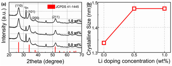
Figure 1.
(a) The Grazing Incidence X-ray Diffraction spectra of SnO2 films and (b) calculated crystalline sizes of SnO2 films as a function of Li (wt%).
Figure 2a–c show the representative O 1s XPS spectra of Li-doped SnO2 as a function of Li (wt%). The O 1s peak was divided into three types of peaks [21]. One peak is for the O2− combined with the adjacent ion in Lattice (OLattice), another for the Oxygen bonds related to the oxygen vacancy (OVacancy), and the other for the amount of OH. Figure 2d shows that the variation in the composition ratio of OVacancy, OLattice, and –OH groups as a function of Li (wt%). When a 0.5 wt% Li dopant was added, the relative percentage of OVacancy gradually decreased from 27.5% to 21.7%, whereas the relative percentage of OLattice gradually increased from 65.7% to 68.1%, which meant that a small amount of Li dopant could work as a carrier inhibitor. Several factors, such as electronegativity, standard electrode potential (SEP), and ion radius, need to be assessed for dopants to be used as carrier inhibitors [22,23]. The electronegativity of dopants and oxygen should significantly differ from each other. When the SEP of the dopant is lower than that of the host, the dopant–oxygen bond becomes stronger. The electronegativity and SEP of Sn hosts and Li dopants were 1.96 and −0.14 V and 0.98 and −3.04 V, respectively. Based on the aforementioned theory, the Li dopant could work as a carrier inhibitor successfully. Moreover, the radius of the dopant and host ions should not differ considerably to avoid the breakdown of the structure; the radii of Sn4+ and Li+ were 74 and 68 pm, respectively, making Li+ suitable as the dopant. However, when 1.0-wt% Li was added, the relative percentage of OVacancy increased from 21.2% to 23.3%, while the relative percentage of OLattice decreased from 68.1% to 66.6%.
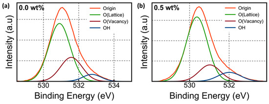
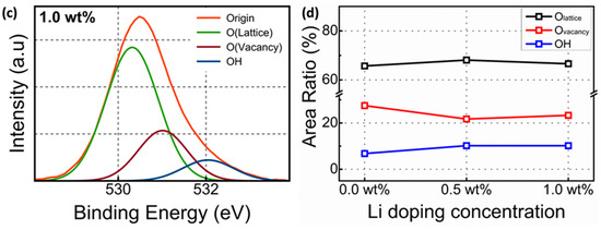
Figure 2.
(a–c) O 1s XPS spectra and O 1s composition area ratio of Li-doped SnO2 and (d) the variation of the composition ratio of OVacancy, OLattice, and –OH groups as a function of Li (wt%).
To elucidate the effect of the Li dopant amount on the optical bandgap of SnO2 films, the transmittance plots of the SnO2 films as a function of Li dopant amounts were obtained using a UV–vis spectrophotometer. Regardless of the Li dopant amount all the fabricated SnO2 films showed a transmittance of >97.5% in the visible range (380–900 nm) (Figure 3a). However, at less than 350 nm, all the SnO2 films showed a drastic decrease in the bandgap absorption, corresponding to the optical bandgap of SnO2 films. The optical bandgap can be obtained by extrapolating the line segment in Figure 3b and using the following equation:
where α is the absorption coefficient, A is a constant, and Eg is the optical bandgap of SnO2 films. For direct bandgap transition, the n value is ½. Using Equation (2), the estimated optical bandgaps of each film were 3.79 eV, 3.87 eV, and 3.93 eV. As a function of Li concentration, the optical bandgap of SnO2 films increased. Regardless of the Li dopant amount, the obtained optical bandgap of the fabricated SnO2 films was larger than that of bulk SnO2 (3.60 eV). If the film thickness was close to the Bohr radius owing to the quantum confinement effect, the optical bandgap could increase. The change in the optical bandgap can be calculated using the following equation [24,25]:
where h is the Plank’s constant, t is the thickness of SnO2 films, me* and mh* are the effective masses of electrons and holes, respectively (for SnO2, me* = 0.275m0, m0 = 9.1 × 10⁻³¹ kg). Because me* << mh*, 1/mh* term can be ignored [24]. Regardless of Li dopant amount, the film thickness was approximately 5.5 nm, and the calculated optical bandgap was 3.90 eV. An additional change in the optical bandgap could be attributed to the free carrier concentration. Figure 3c presents the valence band (VB) spectra of Li-doped SnO2 films using XPS. The VB offset values between the maximum VB value and the Fermi level were extrapolated by linear fitting and the values were 3.65 eV, 3.46 eV, and 3.65 eV, respectively [26]. Using the obtained bandgap and VB offset values, the conduction band (CB) offset values between the minimum of CB value and Fermi level could be calculated. The calculated CB offset values were 0.14 eV, 0.41 eV, and 0.28 eV, respectively, and they were proportional to the carrier concentration. The CB offset value of the 0.5 wt% Li dopant was the lowest, implying the lowest carrier concentration among the three cases by suppressing OVacancy formation, determines the free carrier concentration in the MOS system [27].
Figure 3.
(a) Transmittance spectra of Li-doped SnO2 films as a function of Li (wt%). (b) Optical bandgap of Li-doped SnO2 films as a function of Li (wt%). (c) VB offset based on XPS spectra. (d) Schematic energy band based on the Fermi energy-level position.
Figure 4 shows the electrical characteristics of the fabricated Li-doped SnO2 based TFTs represented by output and transfer curves. The output curve (Figure 4a–c) was probed every 10 V between the gate voltage −30.0 and 30.0 V. Regardless of the Li dopant amounts, all the fabricated SnO2 TFTs showed the conventional n-type semiconductor properties and exhibited a high on/off current ratio (over 107). The relatively large work function of an Au source and a drain electrode on n-type semiconductor results in the formation of Schottky contacts. The nonlinear relationship between drain currents and voltages originates from the abovementioned energy barrier between electrodes and semiconductors [14]. The TFT fabricated using pure SnO2 showed the depletion-mode operation with a negative threshold voltage (Vth). This device, which is in the depletion mode, could easily form a channel at a gate voltage of 0.0 V owing to the presence of excessive free carriers in the SnO2 TFT. However, 0.5- and 1.0-wt% Li-doped TFTs showed the enhancement-mode operation with a positive Vth. Compared with pure SnO2, the reduced OVacancy generated less free carriers, leading to a late turn on. Field effect mobility (FEM) in the saturation regime and Vth were obtained by linear fitting to the (ID)0.5–VG plot using the following equation:
where Ci (insulator capacitance) = , W (channel width) = 1000 μm, L (channel length) = 100 μm. The FEM in the saturation regime of the SnO2 TFT was 5.91 cm2/Vs. The FEM values of the TFTs consisting of 0.5- and 1.0 wt% Li doped SnO2 TFTs were 2.0 and 4.42 cm2/Vs, respectively. Grain boundary scattering, related to the grain boundary number, inside the channel material was strongly affected the FEM of TFTs. For example, a transistor, consisting of channel material, having large crystallinity, showed increased FEM by suppressing the grain boundary scattering [28]. Although based on the GIXRD data, the calculated crystalline size of the pure SnO2 films was smaller than those of the Li-doped SnO2 films, the FEM in saturation regime of pure SnO2 TFTs showed the highest values. For the MOS system, the main transportation mechanism was the percolation conduction mechanism. Based on this mechanism, the FEM could be improved by filling trap sites at high carrier concentrations [29]. The number of free carriers could be increased by forming OVacancy inside MOSs. OVacancy worked as donor levels and generated carriers using the following equation:
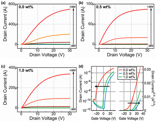
Figure 4.
(a–c) ID–VD curves and (d) transfer curves and ID0.5 vs. VG curves of Li-doped SnO2 based TFTs, as Li (wt%) increases.
The decreased FEM value of 0.5-wt% Li-doped SnO2-based TFT attributed to the decrease in the number of OVacancy, which was confirmed using XPS data. This is a critical factor, compared with grain boundary scattering effects in this system. Additionally, The reduced number of OVacancy was the reason for the low FEM value of the 0.5-wt% Li-doped SnO2-based TFT show compared with that of pure SnO2-based TFTs [16]. The 1.0 wt% Li-doped SnO2 based TFTs again showed increased OVacancy again, and which increased the FEM and induced a negative shift of Vth compared with the 0.5 wt% Li-doped based SnO2 TFTs. It was already reported that Li can be located at the interstitial site and substitutional site in the SnO2 matrix. If Li is located at the interstitial site, this can increase carrier concentration by generating on electron. The increased carrier concentration results in the enhanced FEM, based on aforementioned the percolation conduction mechanism. However, if Li is located at a substitutional site in the SnO2 matrix, it can neutralize the electrons, which are the system’s main carriers; because of fewer electrons, FEM decreases.
Figure 5a–c show the transfer curves of the representative TFT as a function of the negative bias stress (NBS) time with a drain voltage of +5.0 V. During the NBS test, −30.0 V was biased to gate electrodes for 1000 s. Under these NBS conditions, Vth shifts –10.5, 1.32, and 3.81 V, respectively. The extracted ΔVth (5 devices) is plotted in Figure 5d to check the statistical distribution. The 0.5 wt% Li-doped based SnO2 based TFT exhibited the lowest Vth shift among the three cases. Based on XPS data, 0.5 wt% Li-doped SnO2 based TFT showed the lowest OVacancy concentration. Based on the percolation conduction mechanism, the lowest OVacancy leads to the lowest FEM and improved NBS properties. This negatively shifted Vth originated from the tapping of positive charges at the interface between semiconductors and insulators. OVacancy could form VO2+ and 2e−. VO2+ could move to the interface between semiconductors and insulators during the NBS test. By adding the optimal amount Li dopant, the OVacancy could be decreased by the formation of Li–OVacancy pairs, leading to improved NBS properties [18,19,30]. In addition, compared with sol–gel-processed Mg- and Ti-doped based SnO2, Li-doped SnO2 based TFTs show more stable NBS properties [19,30]. Comparing to the previous results, Li-doped SnO2 TFTs show similar or higher field effect mobility and comparable negative bias stability. The reported Si- and Ga-doped SnO2 based TFTs show higher FEM and the Si-doped SnO2 based TFTs show the better NBS properties [31]. Corresponding to deposition method, the crystallinity, chemical composition, and carrier concentration were changed. In this paper, the sol–gel-processed SnO2-based thin film transistors show lower field effect mobility, compared to reported SnO2 semiconductors deposited by the vacuum-based deposition technique. However, sol–gel-processed Li doping can be applied to other types of the solution-processed oxide TFTs.
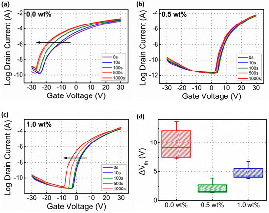
Figure 5.
(a–c) Variation in transfer curves and (d) change in Vth of Li-doped SnO2 based TFTs during NBS test.
4. Conclusions
In this study, sol–gel-processed Li-doped SnO2-based TFTs were fabricated on SiO2/p+ Si substrates. The influence of the Li dopant amount on the structural, chemical, optical, and electrical characteristics of the fabricated Li-doped SnO2-based TFTs was investigated. By adding 0.5-wt% Li, the oxygen vacancy formation process was successfully suppressed. The TFTs fabricated using 0.5-wt% Li-doped SnO2 semiconductor films exhibited FEM in the saturation regime of 2.0 cm2/Vs and showed the enhancement-mode operation. The decreased OVacancy inside the SnO2-based TFTs fabricated using 0.5-wt% Li improved the negative bias stability of TFTs.
Author Contributions
Conceptualization, H.-J.K. and J.J.; experiments and data analysis, H.-J.K., D.-W.K., W.-Y.L.; investigation, S.-H.L., J.-H.B., I.-M.K. and J.J.; writing—original draft preparation, H.-J.K. and J.J.; writing—review and editing, H.-J.K., D.-W.K., W.-Y.L., S.-H.L., J.-H.B., I.-M.K. and J.J. All authors have read and agreed to the published version of the manuscript.
Funding
This research was supported by the Basic Science Research Program through the National Research Foundation of Korea (NRF) grant funded by the Korea government (MSIT) (2019R1F1A1059788).
Data Availability Statement
Data available in a publicly accessible repository.
Conflicts of Interest
The authors declare no conflict of interest.
References
- Nomura, K.; Ohta, H.; Takagi, A.; Kamiya, T.; Hirano, M.; Hosono, H. Room-temperature fabrication of transparent flexible thin-film transistors using amorphous oxide semiconductors. Nature 2004, 432, 488–492. [Google Scholar] [CrossRef] [PubMed]
- Yabuta, H.; Sano, M.; Abe, K.; Aiba, T.; Den, T.; Kumomi, H.; Nomura, K.; Kamiya, T.; Hosono, H. High-mobility thin-film transistor with amorphous InGaZnO4 channel fabricated by room temperature rf-magnetron sputtering. Appl. Phys. Lett. 2006, 89, 112123. [Google Scholar] [CrossRef]
- Tomai, S.; Nishimura, M.; Itose, M.; Matuura, M.; Kasami, M.; Matsuzaki, S.; Kawashima, H.; Utsuno, F.; Yano, K. Highperformance thin-film transistor with amorphous In2O3–SnO2–ZnO channel layer. Jpn. J. Appl. Phys. 2012, 51, 03CB01. [Google Scholar] [CrossRef]
- Ebata, K.; Tomai, S.; Tsuruma, Y.; Iitsuka, T.; Matsuzaki, S.; Yano, K. High-mobility thin-film transistors with polycrystalline in–Ga–O channel fabricated by DC magnetron sputtering. Appl. Phys. Express 2012, 5, 011102. [Google Scholar] [CrossRef] [Green Version]
- Presley, R.; Munsee, C.L.; Park, C.-H.; Hong, D.; Wager, J.; Keszler, D.A. Tin oxide transparent thin-film transistors. J. Phys. D Appl. Phys. 2004, 37, 2810–2813. [Google Scholar] [CrossRef] [Green Version]
- Haxel, G.B.; Hedrick, J.B.; Orris, G.J. Rare Earth Elements—Critical Resources for High Technology; US Department of the Interior, US Geological Survey: Menlo Park, CA, USA, 2002; Volume 87. Available online: https://pubs.usgs.gov/fs/2002/fs087-02/ (accessed on 20 November 2002).
- Bashir, A.; Wöbkenberg, P.H.; Smith, J.; Ball, J.M.; Adamopoulos, G.; Bradley, D.D.C.; Anthopoulos, T.D. High-Performance Zinc Oxide Transistors and Circuits Fabricated by Spray Pyrolysis in Ambient Atmosphere. Adv. Mater. 2009, 21, 2226–2231. [Google Scholar] [CrossRef]
- Allemang, C.R.; Cho, T.H.; OTrejo, O.; Ravan, S.; Rodríguez, R.E.; Dasgupta, N.P.; Peterson, R.L. High-Performance Zinc Tin Oxide TFTs with Active Layers Deposited by Atomic Layer Deposition. Adv. Electron. Mater. 2020, 6, 2000195. [Google Scholar] [CrossRef]
- Jang, B.; Kim, T.; Lee, S.; Lee, W.Y.; Kang, H.; Cho, C.S.; Jang, J. High performance ultrathin SnO2 thin-film transistors by sol-gel method. IEEE Electron Device Lett. 2018, 39, 1179–1182. [Google Scholar] [CrossRef]
- Button, K.J.; Fonstad, C.G.; Dreybrodt, W. Determination of the electron masses in stannic oxide by submillimeter cyclotron resonance. Phys. Rev. B 1971, 4, 4539–4542. [Google Scholar] [CrossRef]
- Bierwagen, O.; Speck, J.S. High electron mobility In2O3 (001) and (111) thin films with nondegenerate electron concentration. Appl. Phys. Lett. 2010, 97, 072103. [Google Scholar] [CrossRef]
- Look, D.C.; Reynolds, D.C.; Sizelove, J.R.; Jones, R.L.; Litton, C.W.; Cantwell, G.; Harsch, W.C. Electrical properties of bulk ZnO. Solid State Commun. 1998, 105, 399–401. [Google Scholar] [CrossRef]
- Jang, J.; Kitsomboonloha, R.; Swisher, S.L.; Park, E.S.; Kang, H.; Subramanian, V. Transparent high-performance thin film transistors from solution-processed SnO2/ZrO2 gel-like precursors. Adv. Mater. 2013, 25, 1042–1047. [Google Scholar] [CrossRef]
- Jang, B.; Kim, T.; Lee, S.; Lee, W.Y.; Jang, J. Schottky nature of Au/SnO2 ultrathin film diode prepared by sol-gel method. IEEE Electron Device Lett. 2018, 39, 1732–1735. [Google Scholar] [CrossRef]
- Lee, W.Y.; Ha, S.H.; Lee, H.; Bae, J.H.; Jang, B.; Kwon, H.J.; Jang, J. Densification control as a method of improving air stability of thin film transistors based on sol-gel processed SnO2. IEEE Electron Device Lett. 2019, 40, 905–908. [Google Scholar] [CrossRef]
- Lee, H.; Ha, S.H.; Bae, J.H.; Kang, I.M.; Kim, K.; Lee, W.Y.; Jang, J. Effect of annealing ambient on SnO2 thin film transistors via an ethanol-based sol-gel route. Electronics 2019, 8, 995. [Google Scholar] [CrossRef] [Green Version]
- Jang, J.; Kang, H.; Chakravarthula, H.C.N.; Subramanian, V. Fully inkjet-printed transparent oxide thin film transistors using a fugitive wettability switch. Adv. Electron. Mater. 2015, 1, 1500086. [Google Scholar] [CrossRef]
- Kim, T.; Jang, B.; Lee, S.; Lee, W.Y.; Jang, J. Improved negative bias stress stability of sol-gel-processed Mg-doped In2O3 thin film transistors. IEEE Electron Device Lett. 2018, 39, 1872–1875. [Google Scholar] [CrossRef]
- Lee, W.Y.; Lee, H.; Ha, S.; Lee, C.; Bae, J.H.; Kang, I.M.; Kim, K.; Jang, J. Effect of Mg Doping on the Electrical Performance of a Sol-Gel-Processed SnO2 Thin-Film Transistor. Electronics 2020, 9, 523. [Google Scholar] [CrossRef] [Green Version]
- Prado, F.; Cremades, A.; Maestre, D.; Ram’ırez-Castellanos, J.; Gonz’alez-Calbet, J.M.; Piqueras, J. Controlled synthesis of lithium doped tin dioxide nanoparticles by a polymeric precursor method and analysis of the resulting defect structure. J. Mater. Chem. A 2018, 6, 6299–6308. [Google Scholar] [CrossRef]
- Chen, S.; Warwick, M.E.A.; Binions, R. Effects of film thickness and thermal treatment on the structural and opto-electronic properties of Ga-doped ZnO films deposited by sol–gel method. Sol. Energy Mater. Sol. Cells 2015, 137, 202–209. [Google Scholar] [CrossRef]
- Lee, S.-H.; Kim, T.; Lee, J.; Avis, C.; Jang, J. Solution processed gadolinium doped indium-oxide thin-film transistors with oxide passivation. Appl. Phys. Lett. 2017, 110, 122102. [Google Scholar] [CrossRef]
- Parthiban, S.; Kwon, J.-Y. Role of dopants as a carrier suppressor and strong oxygen binder in amorphous indium-oxide-based field effect transistor. J. Mater. Res. 2014, 29, 1585–1596. [Google Scholar] [CrossRef] [Green Version]
- Ghosh, S.; Das, K.; Chakrabarti, K.; De, S.K. Effect of oleic acid ligand on photophysical, photoconductive and magnetic properties of monodisperse SnO2 quantum dots. Dalton Trans. 2013, 42, 3434–3446. [Google Scholar] [CrossRef]
- Singh, K.C.B.; Vijay, Y.K. Variation of optical band gap in obliquely deposited selenium tin films. Indian J. Pure Appl. Phys. 2005, 43, 129–131. [Google Scholar]
- Ahn, B.D.; Jeon, H.J.; Park, J.S. Effects of Ga:N Addition on the Electrical Performance of Zinc Tin Oxide Thin Film Transistor by Solution-Processing. ACS Appl. Mater. Interfaces 2014, 6, 9228–9235. [Google Scholar] [CrossRef]
- Yang, Y.; Wang, W.; Yin, S. Oxygen vacancies confined in SnO2 nanoparticles for desirable electronic structure and enhanced visible light photocatalytic activity. Appl. Surf. Sci. 2017, 420, 399–406. [Google Scholar] [CrossRef]
- Gupta, N.; Tyagi, B.P. On-current modeling of polycrystalline silicon thin-film transistors. Phys. Scr. 2005, 72, 339. [Google Scholar] [CrossRef]
- Kim, Y.S.; Park, C.H. Rich variety of defects in ZnO via an attractive interaction between O vacancies and Zn interstitials: Origin of n-type doping. Phys. Rev. Lett. 2009, 102, 806403. [Google Scholar] [CrossRef] [Green Version]
- Lee, W.Y.; Lee, H.; Ha, S.; Lee, C.; Bae, J.H.; Kang, I.M.; Jang, J. Improved negative bias stability of sol–gel processed Ti-doped SnO2 thin-film transistors. Semicond. Sci. Technol. 2020, 35, 115023–115028. [Google Scholar] [CrossRef]
- Jenifer, K.; Arulkumar, S.; Parthiban, S.; Kwon, J.Y. A Review on the Recent Advancements in Tin Oxide-Based Thin-Film Transistors for Large-Area Electronics. Electron. Mater. 2020, 49, 7098–7111. [Google Scholar] [CrossRef]
Publisher’s Note: MDPI stays neutral with regard to jurisdictional claims in published maps and institutional affiliations. |
© 2021 by the authors. Licensee MDPI, Basel, Switzerland. This article is an open access article distributed under the terms and conditions of the Creative Commons Attribution (CC BY) license (https://creativecommons.org/licenses/by/4.0/).