1. Introduction
A unity-gain buffer is an analogue amplifier with a voltage gain equal to 1 V/V. Among these amplifiers there are unity-gain zero-offset buffers characterized by zero offset between input and output voltages [
1,
2,
3,
4,
5,
6,
7,
8]. Unity-gain zero-offset buffers have found application in the testing of analogue chips [
8], in analogue filtering [
9,
10,
11], oscillators [
12], voltage regulators [
13,
14], and in LCD panels [
15,
16]. Most of these buffer solutions use the classic approach based on a high-gain differential amplifier and a negative feedback to obtain unity gain and zero offset. A representative example of the classic approach is the Miller opamp (operational amplifier) with an output connected to an inverting input (
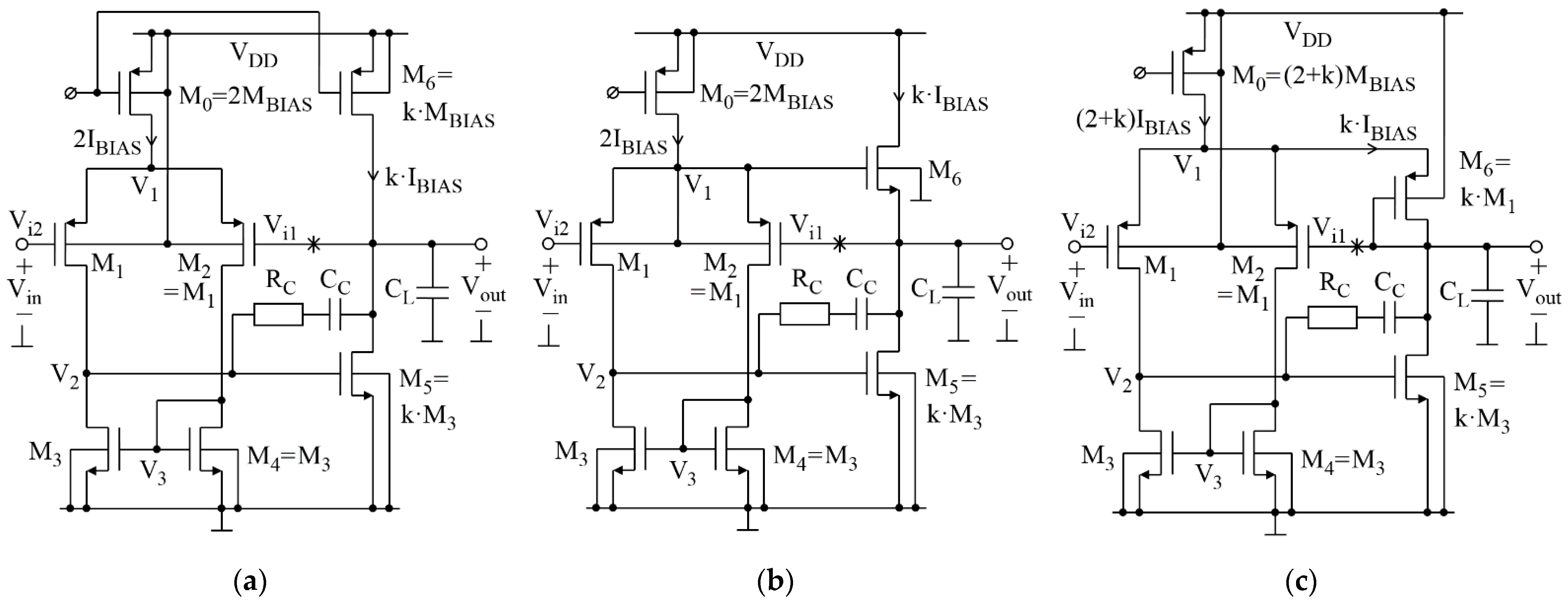
Figure 1a). The advantages of this buffer solution are its relatively simple design, wide input voltage range, and its full compatibility with standard CMOS technologies. Furthermore, since the Miller OpAmp has a high open-loop gain for differential-mode signals, a buffer gain can be very close to 1 V/V. To further reduce the gain error, it was proposed in [
1] to use also a common-mode signal. In this case, a common-mode signal component is forwarded from the input to the output along an additional path. Such a feedforward path for a common-mode signal can be relatively simple to implement by using only one n-channel transistor (M
6 in
Figure 1b). A limitation of such a solution is the need for using an n-channel transistor without the body effect, which is not available in standard CMOS processes. In this paper, an improvement of the solution of [
1] is proposed (
Figure 1c), which gives substantially reduced gain error, improved PSRR, and full applicability in standard CMOS technologies.
The circuits in
Figure 1a–c are studied and the impact on circuit performance from introducing a common-mode feedforward path is examined. To make this study meaningful, key parameters, such as power consumption, load capacitance, bandwidth, and layout area, are assumed to be similar in all three circuits. The results of theoretical analyses and simulations, followed by discussion assuming the circuits realization in 180-nm 1.8-V process of austriamicrosystems AG (ams AG), are presented in the following sections.
2. Theoretical Analysis
The circuits in
Figure 1a–c are closed-loop differential amplifiers with two stages. The first stage is exactly the same in all cases and is composed of the transistors M
1-M
4. The second stage in
Figure 1a,b consists of M
5 loaded by M
6. In
Figure 1c, the second stage can be identified as M
5 loaded by the series connection of M
6 and M
1-M
2. The transistors are sized so that the first and second stages are biased at 2
IBIAS and
kIBIAS, respectively.
Each circuit has a traditional negative feedback loop (the loop breaking point is marked by the symbol *) operating on a differential-mode component of the input signal (
Vi1 −
Vi2). The circuits in
Figure 1b,c also have a positive feedforward loop operating with the common-mode component, (
Vi1 +
Vi2)/2. The common-mode component is generated at node V
1 by the differential pair and is transferred to the output by M
6.
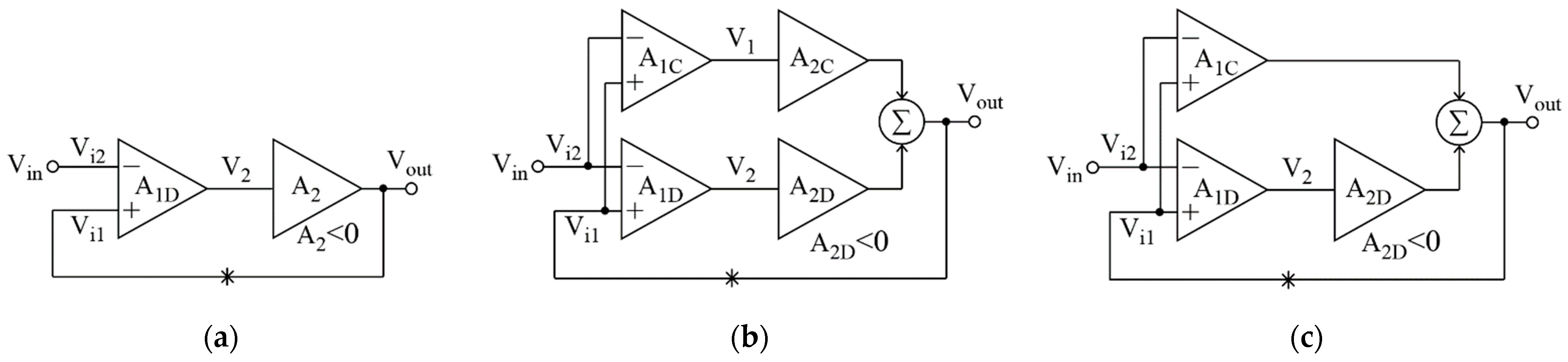
In the following analysis, the common-mode signal at node V2 is omitted because it is suppressed by the first stage due to its symmetry (owing to CMRR).
When the negative feedback loop is opened (broken in the point *), the output small-signal voltage can be determined using the superposition principle [
1]
where
AD and
AC are the small-signal gains for the differential- and common-mode components, respectively.
After closing the loop (
Vi1 =
Vout,
Vi2 =
Vin) the voltage gain becomes
Equation (4) indicates that, as AC is close to 1, the gain error is significantly reduced even though AD is reduced.
The result of applying the superposition principle (1) to each of the circuits in
Figure 1a–c is shown in the corresponding diagrams in
Figure 2a–c.
2.1. Gain Error in the Classic Buffer
The circuit in
Figure 1a processes only the differential-mode component due to the CMRR effect, as mentioned earlier. This means that
AC = 0 and
AD =
A1D·
A2, where
A1D and
A2 are the gains of the first and the second stage, respectively,
where
gm1,2 =
gm1 =
gm2,
gds1,2 =
gds1 =
gds2,
gds3,4 =
gds3 =
gds4, and
The gain error in (7) can be relatively small because the product |A1D·A2| ranges from 102 to 103, depending on IBIAS and transistor sizes.
2.2. Gain Error in the Buffer of Figure 1b
The circuit in
Figure 1b processes differential- and common-mode components, as shown in
Figure 2b. The differential signal path (
A1D followed by
A2D) is the same as in the classic circuit, but the gain of the second stage (
A2D) is lower and is close to −1.
The common-mode signal passes, firstly, through the differential pair to node
V1 and, next, through the source follower M
6 to the buffer output. The particular gains of the common-mode feedforward path are
and
where
A2C is the gain of the follower M
6. Note that in a typical CMOS process,
A2C is about 0.8 V/V, because the transconductance ratio in M
6 (
gmb6/
gm6) is close to 0.2. Therefore, the common-mode signal is forwarded to the buffer output with a gain less than 1 (
AC =
A1C·
A2C < 1).
Hence, the buffer gain is
As A1D and gm5 in (11) are the same as in (7), the gain error is larger than in the classic solution because of the body effect of M6 (because gmb6 is larger than gds6 + gds5).
2.3. Gain Error in the Proposed Buffer
In the proposed buffer (
Figure 1c), the NMOS source follower (M
6) is replaced by a PMOS voltage shifter, i.e., the diode-connected PMOS FET. Thus, the body effect of M
1-M
2 and M
6 cancels each other out, and the common-mode component is transferred to the output with a gain theoretically equal to 1,
Furthermore, the gain of the differential path is higher than that of the circuit in
Figure 1b, as M
5 is loaded by a higher resistance resulting from the series connection of M
6 and M
1-M
2.
Comparing (14) and (7), it can be seen that the gain error of the proposed solution can be lower than the classic one due to the fact that A1C is 1.
2.4. Output Resistance
The output resistances (
Rout) of the considered buffers are practically the same as it is determined mainly by
gm5 and
A1D. In detail, the output resistance of the classic buffer is
For the buffer of [
1] it is
And, for the proposed one the output resistance is
where 1/
gx ≅ 1/(
gm6 +
gmb6) + 0.5/(
gm1,2 +
gmb1,2).
2.5. Power Supply Rejection Ratio
Supply interference paths, from
VDD to
Vout, are different in each of the buffers. In the buffer in
Figure 1a,
VDD interference passes to
Vout in three ways: through M
0 (
gds0), M
1,2 (bulk), and M
6 (
gds6). The output conductance of M
6 (
gds6) together with
Rout form a resistive divider. Since 1/
gds6 >>
Rout, interference passing through
gds6 to
Vout is suppressed.
VDD interference passing through M
0 and M
1,2 is attenuated in the first stage, owing to CMRR.
In the circuit in
Figure 1b, as M
1,2 bulk is not connected to
VDD, the supply interference passes in two ways: through M
0 (
gds0) and M
6 (
gds6). Interference that passes through
gds6 is suppressed, similar to
Figure 1a. Nevertheless, the interference that passes through
gds0 is not suppressed at all because the follower M
6 transfers it from node
V1 directly to
Vout. Since
V1 interference is at a comparable level to that in the circuit of
Figure 1a, the feedforward path formed by M
6 causes PSRR degradation.
In the buffer in
Figure 1c,
VDD interference goes in one way only, through
gds0, because transfer through M
1,2 and M
6 bulks is suppressed due to the body effect compensation, as mentioned earlier. Interference from
VDD passes through
gds0 to
V1 and, next, this interference is transferred by the shifter M
6 directly to
Vout. However, in opposite to
Figure 1b, M
6 is a diode-connected transistor and, thereby, its conductance (
gm6), together with
gds0,
gm1,2 and
Rout, compose a divider that substantially attenuates
V1 interference. As a result, the level of
V1 interference in the circuit in
Figure 1c is much lower than in
Figure 1a. Since there is no another path of interference, a higher PSRR than in the circuit in
Figure 1a can be obtained. Above conclusions are confirmed by simulation results in the next section where detailed values of PSRR of each of the buffers are presented in a performance summary.
3. Simulations
The example designs of the buffers in
Figure 1a–c were made for testing analogue chips (for buffering and monitoring internal analogue nodes). Therefore, a
CL of 12 pF is assumed as it is a capacitance of a typical oscilloscope probe (also such value of
CL was used in [
1]). The transistor scaling factor
k is set to five due to Miller compensation requirements. In a practical two-stage opamp, proper compensation is possible when the transconductance of a second stage is at least five times larger than in a first stage.
IBIAS is set to 100 µA, which results from limiting the power supply to 1 mW at a supply voltage of 1.8 V. The sizes of the transistors are given in
Table 1. The 1.8-voltage standard-
VTH transistors with
VTHP ≈ −0.4 V and
VTHN ≈ 0.45 V were used.
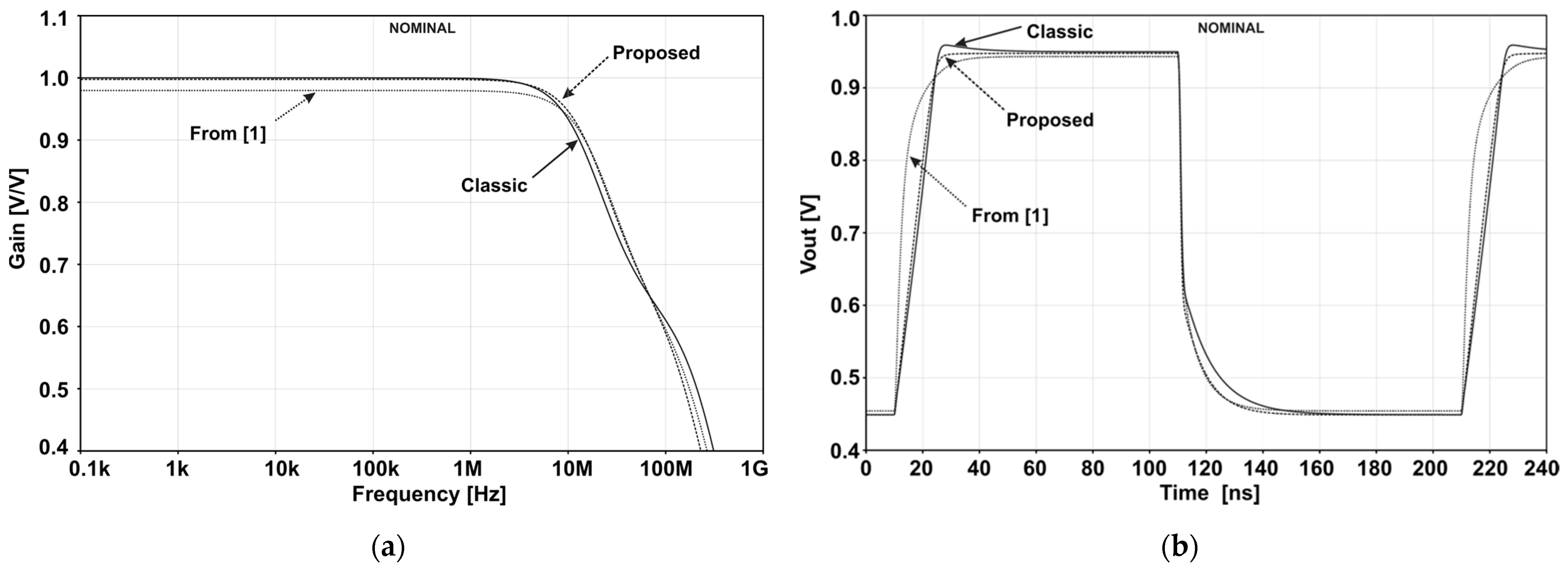
The buffers were compensated to obtain similar −3-dB frequencies in small-signal characteristics (
Figure 3a) as well as minimal overshoots under pulse excitation (
Figure 3b). The applied values of the compensating elements, R
C and C
C, are given in
Table 1. Some small overshoot still exists in the classical buffer impulse response, and of course this can be suppressed, but then the −3-dB frequency will be lower. The circuit of [
1] features the best positive slew rate (SR+), but it results from the fact that the increase in gain error causes an increase in
IDS6 (the larger the difference in
Vin −
Vout, the larger
VGS6 becomes).
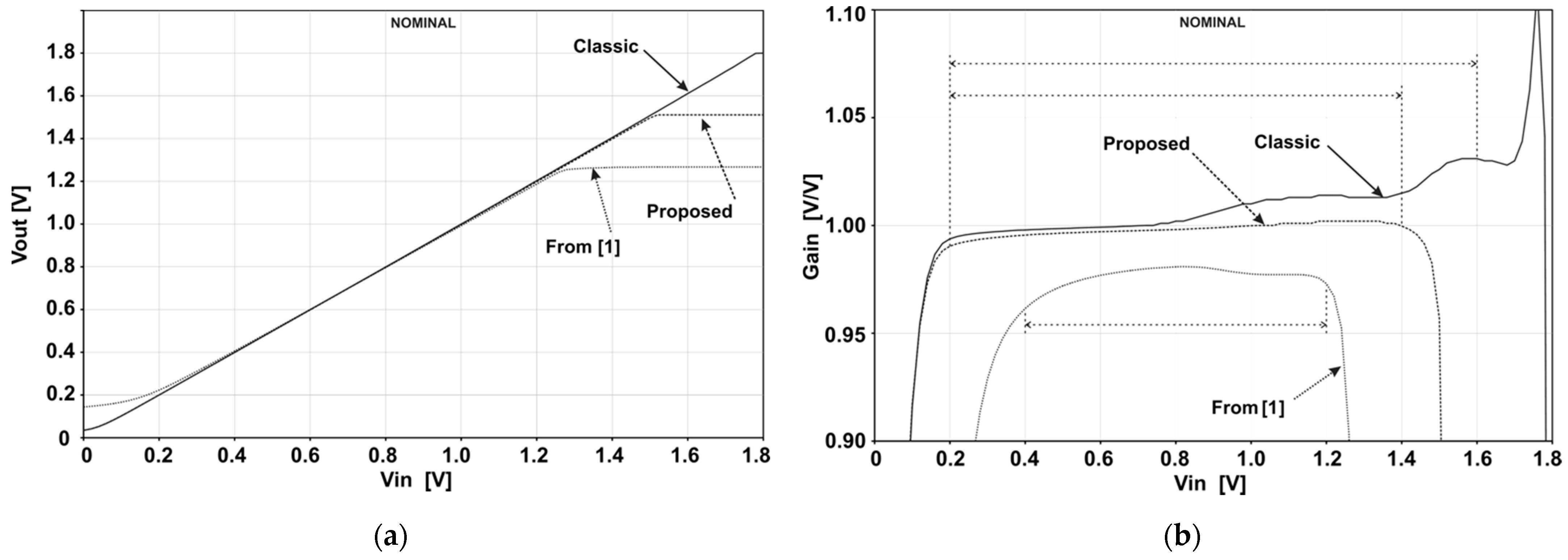
The detailed characteristic of the gain error can be determined directly from a derivative of the static responses in
Figure 4a. The gain error is the deviation of the derivative from 1, i.e.,
gain error = d
Vout/d
Vin − 1. The plots of derivatives presented in
Figure 4b show that, for low
Vin, the classic solution has the smallest gain error. However, the gain error integrated across the entire available input range is the smallest in the proposed circuit (the available ranges are marked in
Figure 4b and are determined by the boundaries beyond which the derivatives sharply change their value). The integrated gain errors are 1.2%, 2.3%, and 0.3% for the classic, from [
1], and proposed circuits, respectively.
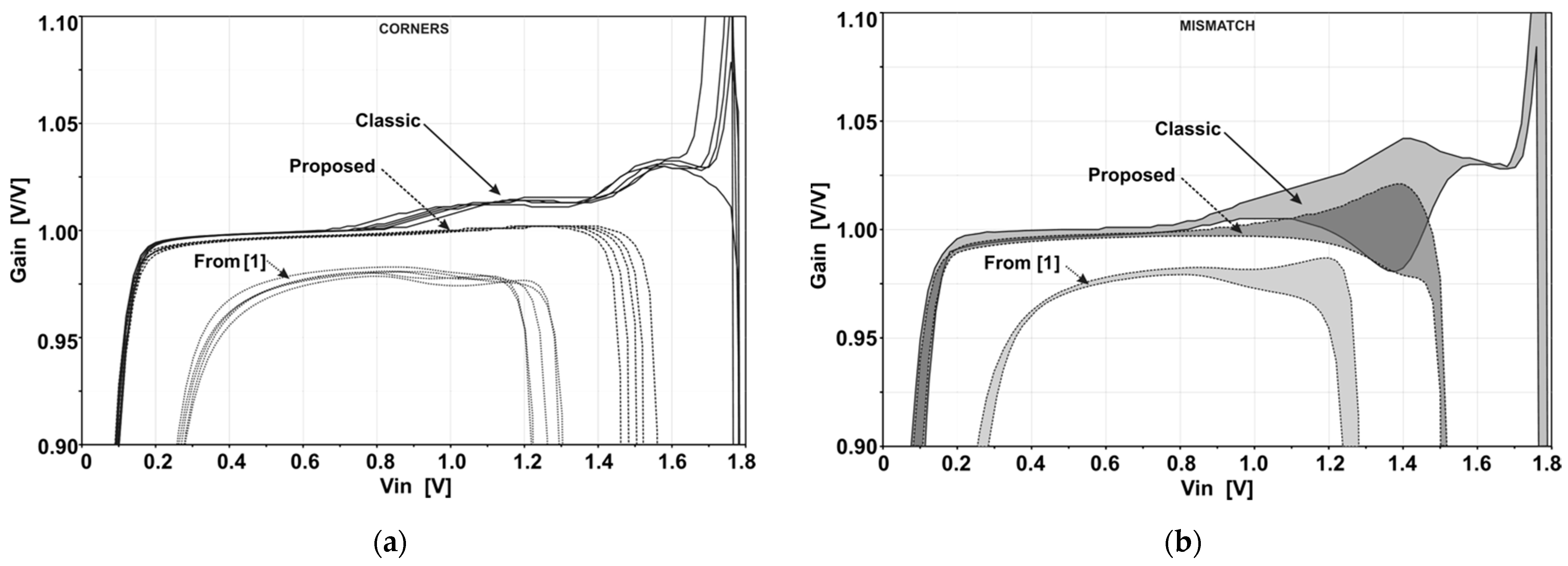
The influence of the process spread and mismatch on the gain is depicted in
Figure 5a,b, respectively. All the buffers show a relatively small sensitivity to process spread. However, the mismatch increases the gain error near the upper boundaries of the input ranges.
The process spread and the mismatch also cause an offset between
Vout and
Vin.
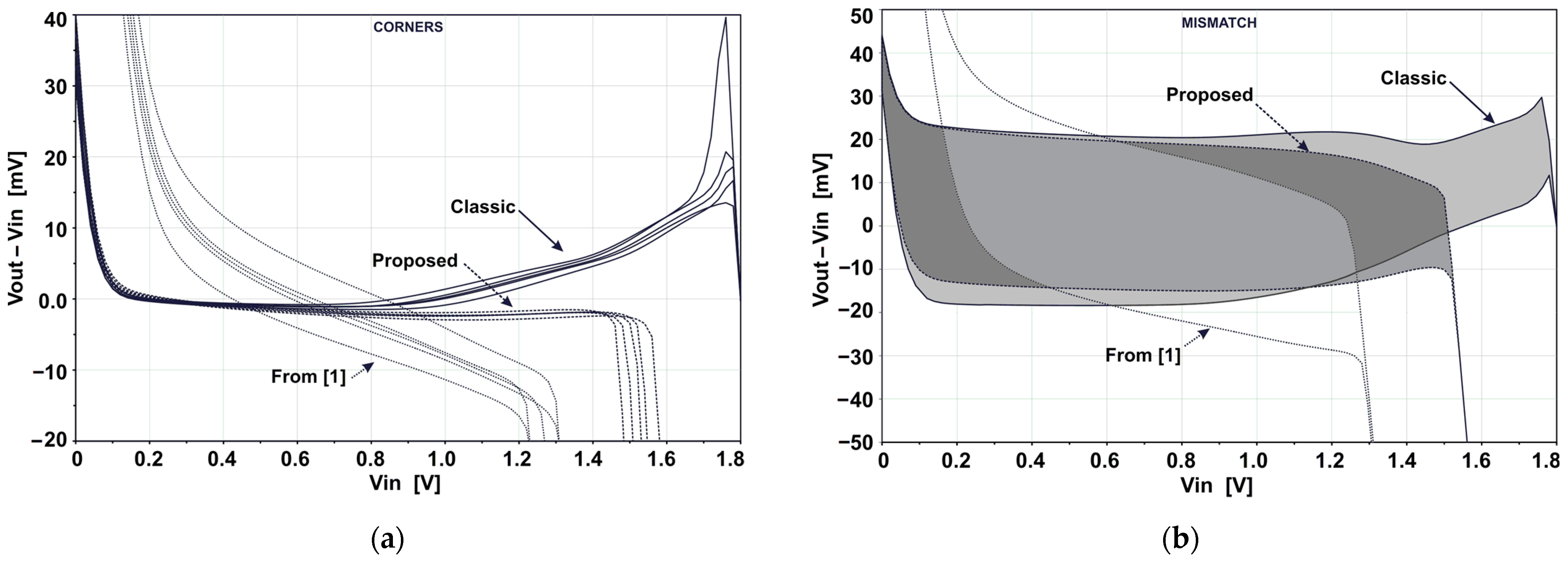
Figure 6a,b show the difference (
Vout −
Vin) under conditions of process spread and mismatch, respectively. Note that (
Vout −
Vin) contains both the offset and gain errors. However, (
Vout −
Vin) is dominated by the offset error. The process-induced offset (
Figure 6a) is the highest in the topology of [
1] because M
1-M
2 and M
6 are opposite-type. On the other side, the mismatch-induced offset (
Figure 6b) is similar in all of the topologies because it is determined mainly by the matching of transistors in the first stage. An aggregated (process + mismatch induced) offset is comparable in all the topologies, and is 6.58 mV, 6.29 mV, and 6.48 mV (1 sigma) for the circuits in
Figure 1a–c, respectively.
The buffers parameters are summarized in
Table 2. In accordance with the design goal, similar power consumption, bandwidth, and occupied area were achieved. Furthermore, the output resistance and noise are practically the same. In these conditions, the classic buffer has the widest DC input range (0.2–1.6 V) and a moderate gain error (1.2%). The proposed solution features an input range (0.2–1.4 V) that is narrower by 200 mV, but the gain error (0.3%) is four times smaller. Moreover, the PSRR (72 dB) is about 20 dB better.
4. Discussion (Circuit Design Principle and Trade-Off)
In this paper, an improved version of a unity-gain zero-offset buffer, which uses an additional feedforward path for a common-mode signal component, is proposed. This modification results in an improvement of some parameters while maintaining circuit complexity similar to the classic Miller OpAmp. The principles of optimization of power consumption, bandwidth, and stability are still the same as in the classical solution. This fact greatly facilitates design of the proposed circuit. Selection of circuit component parameters, depending on design requirements, is carried out in the traditional way. For example, in order to achieve a small offset between Vout and Vin, it is necessary to reduce mismatch of threshold voltages in the input differential-pair transistors M1,2 (due to the fact that Vout = Vin +Vsg1 − Vsg2). Reduction in offset involves using large transistors in the differential pair. Noise optimization requires the reduction in noise from dominant sources, i.e., from the current mirror (M3,4) and from M1,2. In all three buffers designed in this work, contributions from M3,4 and M1,2 to the total buffer noise are 80% and 10%, respectively. The contribution from the current mirror is highest because gates of M3,4 (i.e., noise sources at M3,4 gates) are at a node (V3) of highest gain to Vout (i.e., Vout/V3 is higher than Vout/V2, Vout/V1, and Vout/Vin).
The proposed common-mode feedforward, when applied to the classic buffer, reduces its input voltage range, but improves its gain error and PSRR. Thus, the choice of an appropriate buffer variant depends on the trade-off between input range, gain error, and PSRR. From the point of view of speed performance (slew rate, settling time, overshoot, etc.), it is worth considering the solution from
Figure 1b. In this circuit, the n-channel output stage gives a higher slew rate than achievable using the mixed p-n-channel stages in the classic and proposed buffers. Note that the solution in
Figure 1b would also allow for low gain error if implemented in a triple-well or silicon-on-insulator process, where there is no body effect in the n-channel M
6 transistor. On the other hand, stage arrangements in the classic and proposed buffers are less sensitive to process variations because the first and second stages are better matched, as M
1,2 and M
6, and M
3,4 and M
5, have the same channel type.


 ,
, 

