Abstract
In the post-Moore’s Law era, conventional Von Neumann architectures face critical limitations, such as the “memory wall” and excessive power consumption, particularly when processing unstructured data. Neuromorphic computing, inspired by the human brain, offers a promising solution through parallel processing and adaptive learning. Among the candidates for artificial synapses, memristors based on two-dimensional MXenes (specifically Ti3C2Tx) have attracted significant attention due to their unique layered structure, high metallic conductivity, and tunable physicochemical properties. This review provides a comprehensive analysis of MXene-based memristors, from material synthesis to system-level applications. We examine how different synthesis strategies, including etching methods, directly influence device performance and elucidate the underlying resistive switching mechanisms driven by ion migration, valence change, and interfacial processes. Furthermore, the review demonstrates the efficacy of MXenes in emulating biological synaptic functions—such as spike-timing-dependent plasticity (STDP) and long-term potentiation/depression (LTP/LTD)—and their application in tasks like handwritten digit recognition. Finally, we highlight emerging frontiers in flexible electronics and in-sensor computing, offering insights into the future trajectory of integrated sensing, memory, and computation.
1. Introduction
The rapid development of artificial intelligence (AI) and the Internet of Things (IoT) has imposed extraordinary demands on the computing power and energy efficiency of devices. In recent years, enhancements in language model performance have predominantly coincided with the exponential increase in computational capacity for training [1] (as illustrated in Figure 1). Currently, conventional digital computing systems segregate storage units from processing units, leading to significant energy consumption and slowness in data transmission, a phenomenon referred to as the “von Neumann bottleneck”. Lu et al. estimate that data movement energy consumption may constitute 60% to 90% of the total energy expenditure in the computing process [2]. Figure 2 illustrates a graphical representation of the “von Neumann bottleneck.”
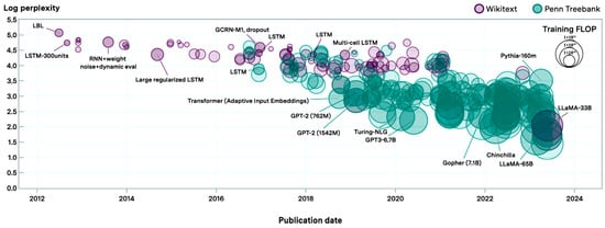
Figure 1.
Training computational power is experiencing explosive growth. Reprinted with permission from Ref. [1]. Copyright 2024 Anson Ho et al.
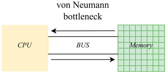
Figure 2.
The CPU and memory transfer data via the bus.
In contrast, the human brain contains roughly 1011 neurons and 1015 synapses, allowing it to execute intricate cognitive functions with minimal power usage (approximately 20 W) and exhibiting remarkable energy efficiency of several million trillion analogue operations per watt (TAOPS/W) [3]. Consequently, it is essential to create neuromorphic devices that replicate the functions of organic synapses and neurons. Neuromorphic systems can significantly reduce data transmission expenses and enhance energy efficiency and parallel processing capabilities by closely integrating computing and storage, while employing event-based sparse distributed information encoding [4]. This design is anticipated to transform contemporary computer systems and demonstrate significant benefits, particularly in tasks like pattern recognition, perception, and adaptive learning [4]. While Phase-Change Memory (PCM) technology has been widely explored for neuromorphic computing applications owing to its mature large-scale integration and multi-level storage capabilities [5], it continues to face critical challenges regarding high switching energy consumption and resistance drift [6].
To achieve the previously mentioned neuromorphic systems with superior energy efficiency and parallel processing capacities, it is essential to create a hardware basis that can replicate the dynamic behaviours of biological synapses and neurons. In this context, memristors, as a novel category of electrical devices, exhibit significant potential for the realisation of neuromorphic capabilities. They are passive two-terminal dynamic devices whose resistance values can be altered based on the history of the charge passing through them or the voltage provided, and this state can be preserved even after power is disconnected. Theoretically introduced by Professor Leon O. Chua in 1971, this notion is defined as the fourth fundamental circuit element, succeeding resistors, capacitors, and inductors [7]. Jo et al. built a nanoscale memristor utilising silver/amorphous silicon (Ag/Si) (Figure 3a,c) and proved that a hybrid system including CMOS neurons and memristor synapses (Figure 3b) can perform essential synaptic functions, notably spike-timing-dependent plasticity (STDP) (Figure 3d) [8].
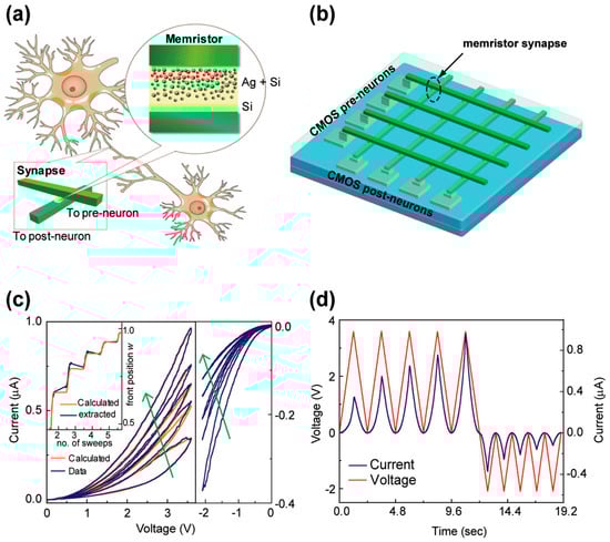
Figure 3.
Device structure and working principle. (a) Schematic illustration of the concept of using memristors as synapses between neurons. The insets show the schematics of the two-terminal device geometry and the layered structure of the memristor. (b) Schematic of a neuromorphic with CMOS neurons and memristor synapses in a crossbar configuration. (c) Measured (blue lines) and calculated (orange lines) I−V characteristics of the memristor. Inset: calculated (orange lines) and extracted (blue lines) values of the normalized Ag front position w during positive DC sweeps. (d) The current and voltage data versus time for the device in (c) highlighting the change in current in sequential voltage sweeps. Reproduced with permission from [8]. Copyright 2010, American Chemical Society.
Two-dimensional (2D) materials offer novel solutions to the performance limitations encountered by conventional memristors, owing to their distinctive atomic-scale architectures and physicochemical characteristics. Their application benefits in memristors are mostly evident in three areas: intrinsic material characteristics, device efficacy, and functional enhancement. They have emerged as a pivotal material system propelling the advancement of high-energy-efficiency neuromorphic computing and next-generation memory technologies [9]. The epoch of 2D materials commenced when Novoselov and Geim adeptly exfoliated monolayer graphene from graphite using the “scotch tape method”. Notwithstanding its superior electrical conductivity, graphene’s absence of a band gap constrains its utility in logic circuits. Consequently, the Mak team created MoS2, a prototypical two-dimensional semiconductor, and elucidated the impact of dimensionality on its band structure. It was observed that as MoS2 crystals are reduced from multilayer to monolayer, a change from an indirect band gap to a direct band gap takes place, resulting in substantial fluorescence increase [10]. This marked the beginning of research on 2D semiconductor optoelectronics. In addition to natural layered materials, MXenes were developed by selectively etching the A-layer (typically aluminium) from MAX phases [11].
The precursor of MXenes is a layered ceramic material known as MAX phase, whose general chemical formula is Mn+1AXn (e.g., Ti2AlC). Herein, the M layer consists of transition metals (e.g., Ti, V, Nb), serving as the skeleton of MXene; The A layer consists of main-group elements (e.g., Al, Si, Ga), serving as the “interlayer”; the X layer comprises carbon, nitrogen (C/N) (Figure 4). It is important to note that layered transition metal borides are distinct materials known as MBenes, derived from MAB phases, and are structurally analogous but chemically different from MXenes [12].
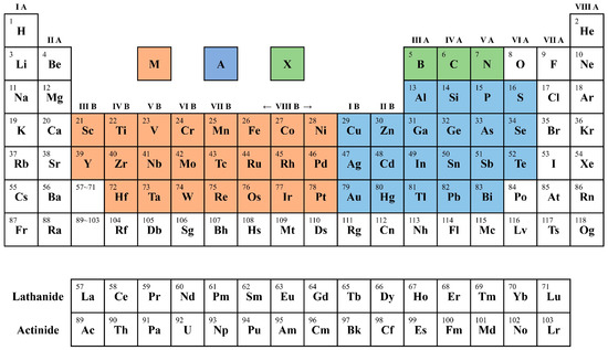
Figure 4.
The MAX element range, where orange represents the M element, blue represents A, and green represents X. Reprinted with permission from Ref. [12]. Copyright 2025 Zhiyao Lu et al.
Researchers chemically remove the A layer from the MAX phase, resulting in the residual layered structure known as MXene. In contrast to other prevalent two-dimensional (2D) materials like graphene and transition metal dichalcogenides (TMDs, e.g., MoS2), the primary and distinctive advantage of MXenes is their exceptional amalgamation of metallic-level electrical conductivity and hydrophilicity. The surface of MXenes is adorned with numerous hydrophilic functional groups (-OH, -O, -F), imparting exceptional hydrophilicity and water dispersibility, equivalent to that of clay. Consequently, MXenes can be readily synthesised into aqueous inks for processing methods such as spin-coating and inkjet printing [13]. Simultaneously, their inner transition metal carbide structure maintains a metal-like high electrical conductivity of up to 20,000 S/cm. The uncommon “conductive and hydrophilic” characteristic of 2D materials enhances their exceptional efficacy in electromagnetic shielding and volumetric specific capacitance, in conjunction with a comparatively high density. Furthermore, swift ion intercalation and deintercalation are facilitated between their layers, where pseudocapacitive reactions transpire. This allows MXene electrodes to attain a volumetric specific capacitance of up to 900 F/cm3 [14], much surpassing that of graphene and conventional activated carbon electrodes, rendering them exceptionally appropriate for small supercapacitors.
Confronted with the pressing need for enhanced computing power and energy efficiency in the age of artificial intelligence (AI) and the Internet of Things (IoT), the issues of “power wall” and “memory wall” arising from the disjunction of storage and computation in the conventional von Neumann architecture have become increasingly salient. Motivated by the remarkable efficiency of the human brain, memristor-based neuromorphic computing has surfaced as a major technological avenue to overcome this limitation. In the investigation of materials for fabricating high-performance memristors, two-dimensional materials have garnered significant interest owing to their distinctive quantum confinement effects and physical characteristics. MXenes, a novel category of 2D transition metal carbides/nitrides, demonstrate unique advantages that set them apart from graphene and TMDs: they feature a 2D layered architecture originating from the etched MAX phase, while seamlessly combining metal-level high conductivity with clay-like hydrophilicity. This addresses the inadequate processability of conventional 2D materials while delivering superior volumetric specific capacitance. These attributes make MXenes a highly interesting candidate material for the development of next-generation neuromorphic devices characterised by low power consumption and high parallelism.
2. Synthesis, Modification, and Structural Engineering of MXene Materials
The physicochemical characteristics of MXenes, including as electrical conductivity, work function, interlayer spacing, and surface active sites, directly influence their efficacy in memristors and neuromorphic computing systems. In contrast to conventional semiconductor materials, MXenes constitute a class of materials that may be extensively tailored using synthetic methods—specifically top-down synthesis and an alternative known as bottom-up synthesis—as well as post-treatment modification. This section will systematically examine the synthetic pathways of MXenes, encompassing a detailed comparison of complete and partial etching strategies, as well as an extensive analysis of the regulatory mechanisms of oxidation engineering, doping engineering, and interface modification on the efficacy of neuromorphic devices.
2.1. Top-Down Synthesis Strategy
2.1.1. High-Concentration Hydrofluoric Acid Etching
This is the initial synthesis technique, utilising Ti3AlC2 as the precursor for MXene and conducting etching with high-concentration hydrofluoric acid (30–50 wt.%) (the reaction process is depicted in Figure 5a–c). Hydrofluoric acid can selectively etch the aluminium layer in Ti3AlC2 while maintaining the integrity of the transition metal carbide/nitride framework. From a microscopic morphological standpoint, the effectively etched product displays a characteristic accordion-like multilayer structure and is abundant in -F and -OH groups on its surface. The intense character of the reaction typically results in the introduction of a considerable number of vacancy defects within the Ti atomic layers. While faults are typically viewed as detrimental, in memristors, these defect sites can frequently act as nucleation sites for the development of conductive filaments, hence contributing to a reduction in forming voltage [11].
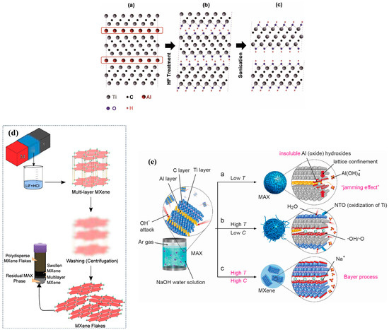
Figure 5.
Different strategies for MXene etching methods. (a–c) Reproduced with permission [11]. Copyright 2011 WILEY-VCH Verlag GmbH & Co. KGaA, Weinheim. (d) Reprinted from Ref. [15] Copyright 2024 Henrique Teixeira et al. (e) Reproduced with permission [16] © 2018 Wiley-VCH Verlag GmbH & Co. KGaA, Weinheim.
Its core chemical reaction equation is generally expressed as follows:
Ti3AlC2 + 3HF→Ti3C2 + AlF3 + 1.5H2
Ti3C2 + 2H2O→Ti3C2(OH)2 + H2
Ti3C2 + 2HF→Ti3C2F2 + H2
2.1.2. In Situ HF Generation Etching
To circumvent the direct application of dangerous high-concentration HF, researchers have devised and implemented a method that produces HF in situ through a mixed solution of LiF and HCl [15,17] (the reaction mechanism is depicted in Figure 5d). In contrast to the direct application of high-concentration HF, this technique offers the benefits of more moderate reaction conditions, as well as increased flake sizes and reduced flaws in the produced MXenes. Leveraging the intercalation effect, Li+ ions in the solution are spontaneously inserted between MXene layers during the etching process, facilitating the acquisition of monolayer or few-layer MXene dispersions through manual shaking or low-power ultrasonication in following stages.
MXenes synthesised with the in situ HF production process typically have enhanced electrical conductivity, reaching approximately 20,000 S/cm. This attribute is beneficial for electrode materials necessitating low contact resistance; nonetheless, when utilised as the resistive switching layer in memristors, excessively high conductivity may diminish the on/off ratio of the devices. Consequently, for memristive applications, further treatments are typically necessary to moderately diminish their electrical conductivity [18].
2.1.3. Molten Salt Etching
Atomic vacancies typically arise during the HF etching of MAX phases. Furthermore, the application of fluorine (F)-containing solutions invariably results in the incorporation of -F functional groups on the product surface, which is challenging to properly control. Kamysbayev et al. effectively generated Ti3C2Cl2, Ti2CCl2, and Nb2CCl2 MXenes by etching Ti3AlC2 MAX phase in molten ZnCl2 and various other Lewis acidic molten salts at 500 °C [19]. Modifying the etching temperature and time allows for the regulation of surface functional groups, hence facilitating the targeted enhancement of the materials’ electrochemical characteristics.
2.1.4. High-Concentration Hot Alkaline Solution Etching
To satisfy the etching criteria for acidic A-layer elements, pertinent research has suggested a fluorine-free, high-concentration hot alkaline solution hydrothermal etching technique, modelled after the Bayer process utilised in bauxite refining [16]. Multilayer Ti3C2Tx MXene, with a purity of 92 wt.%, was effectively synthesised from Ti3AlC2 MAX phase powder via etching in a 27.5 M high-concentration aqueous NaOH solution at 270 °C in an argon-protected environment [16]. The reaction mechanism is illustrated in Figure 5e.
2.1.5. Mechanochemical Synthesis Strategy
Mechanochemical synthesis, particularly ball milling, offers a greener, solvent-free, or low-solvent alternative that leverages mechanical shear forces to facilitate the peeling of the A-layer. Theoretical calculations based on density functional theory (DFT) by Guo et al. [20] revealed that under tensile and shear deformation, the M–Al bonds in MAX phases (e.g., Ti3AlC2, Nb2AlC) are more prone to breakage than the strong M–X bonds. Specifically, shear deformation leads to significant slipping between the Al and M2C layers, providing a microscopic theoretical basis for mechanically exfoliating MXenes from MAX phases [20].
Experimentally, high-energy mechanical milling (HEMM) has proven effective in achieving high-yield delamination. Wu et al. demonstrated a scale delamination method by milling Ti3AlC2 in the presence of dimethyl sulfoxide (DMSO). The DMSO acts as an intercalation agent and an antioxidant, preventing the oxidation of MXenes during the high-energy impact, thereby producing few-layer Ti3C2Tx nanosheets with enhanced electrochemical properties for sodium-ion batteries [21]. Furthermore, to eliminate fluorine contamination entirely, Xue et al. developed a chemical-combined ball-milling strategy using an alkaline etchant (TMAOH) and LiCl. In this process, the mechanical force destroys the passivation layer on the MAX phase, allowing the alkali to continuously etch the Al layer via pitting corrosion. This fluorine-free method yielded MXenes with a unique hierarchical porous structure (P-Ti3C2), exhibiting a specific surface area eight times higher than that of HF-etched samples, which is highly advantageous for ion transport and storage applications [22].
2.2. Bottom-Up Synthesis Strategy
The current approach employed for this synthesis strategy is chemical vapour deposition (CVD), a thin-film fabrication technique that deposits solid materials by chemical reactions of gaseous precursors on a substrate’s surface. The process primarily encompasses the transport and adsorption of precursors, surface chemical reactions and nucleation, along with the desorption and expulsion of by-products. This process offers homogeneous film formation, adjustable composition and thickness, superior coverage, and suitability for large-area and difficult substrates, making it extensively utilised in the fabrication of thin films, coatings, low-dimensional materials, and functional devices.
Wang et al. initially achieved the direct synthesis and morphological regulation of two-dimensional carbide and nitride MXenes by chemical vapour deposition (CVD). The study utilised titanium foil as both the substrate and titanium source, titanium tetrachloride (TiCl4) as the halogen source, and either methane (CH4) or nitrogen (N2) as the carbon or nitrogen source, respectively. The reaction was conducted at elevated temperatures (e.g., 950 °C) and atmospheric pressure [23]. Through meticulous regulation of the precursor flow rate, reaction temperature, and duration, they effectively synthesised vertically oriented, carpet-like Ti2CCl2 MXene films, and subsequently observed intricate morphologies, including multi-layer bending and hollow vesicle-like structures generated by growing stress. This CVD technique is suitable to the synthesis of MXenes that are challenging to produce using conventional etching procedures, such as Zr2CCl2 and the initially reported chlorine-terminated nitride Ti2NCl2, highlighting its significant advantages in component expansion and structural design [23].
2.3. Partial Etching Engineering
The conventional perspective posits that the total elimination of the Al layer is essential for the preparation of high-quality MXenes. Recent studies by research teams indicate that “incomplete etching” may yield unforeseen performance enhancements in neuromorphic computing applications.
Gosai’s research team discovered that the full removal of the Al layer from Ti3C2Tx, followed by intercalation with DMSO (dimethyl sulfoxide), results in a substantial expansion of the interlayer spacing of MXenes. The increased interlayer spacing and the incorporation of DMSO molecules provide a significant energy barrier between the layers, resulting in a configuration akin to a “Multiple Quantum Well”. Regarding device architecture, carriers must surmount a significant potential barrier to transition, leading to an exceptionally high SET voltage of the device (about 4.1 V–7 V). This not only elevates power consumption (~0.128 μJ/mm2) but also constrains its applicability in low-power neuromorphic electronics [24].
Researchers prepared partially etched MXenes with around 8% Al retention by meticulously regulating the reaction duration and acid concentration (Figure 6). This change further modified their structural properties: the leftover Al atoms functioned as “Conductive Bridges,” linking adjacent Ti3C2 layers, so effectively mitigating the excessive growth of interlayer space and diminishing the potential barrier for electron transit between layers. Simultaneously, the device’s performance experienced a qualitative transformation: the SET voltage was diminished to 1.0 V or lower. The energy consumption each pulse was reduced to 1.36 nJ/mm2, and the mechanical stability was markedly enhanced. The leftover aluminium atoms augmented the mechanical resilience of the multilayer structure, resulting in negligible loss of the device’s electrical performance after 1000 bending cycles at an angle of 73° [24].
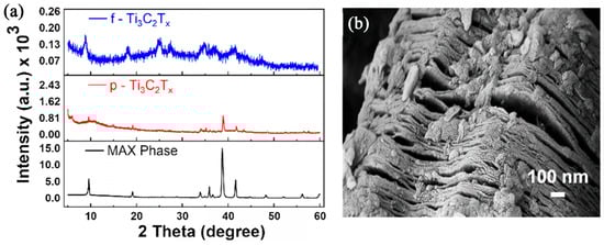
Figure 6.
(a) XRD analysis of MAX phase, partially etched (p-Ti3C2Tx) and fully etched (f-Ti3C2Tx) MXene. (b) Field emission scanning electron microscopy (FE-SEM) image of the Ti3C2Tx powder. Reproduced with permission from [24]. Copyright 2024, American Chemical Society.
This partial etching technique, as a significant advancement in material engineering, facilitates novel applications of MXenes in low-power neuromorphic computer devices.
2.4. Oxidation Engineering and Heterostructure Construction
Oxidation of Ti3C2Tx in humid settings is typically considered a form of instability; nevertheless, in neuromorphic devices, regulated oxidation has been repurposed as a technique for fabricating high-performance resistive switching layers.
2.4.1. Hydrothermal In Situ Oxidation
Kundale et al. exhibited a methodology for the in situ synthesis of TiO2 nanocrystals on the MXene surface by the hydrothermal technique (Figure 7a). MXene dispersions underwent treatment at elevated temperature and pressure, resulting in the oxidation of certain titanium atoms into anatase TiO2. The procedure led to the creation of a Ti3C2Tx/TiO2 micro-heterojunction (Figure 7b–i). This configuration preserves the highly conductive core of MXene while employing the TiO2 shell to offer many oxygen vacancies. The movement of oxygen vacancies within the TiO2 layer constitutes the primary resistive switching mechanism, hence augmenting the valence change memory (VCM) mechanism and enhancing the on/off ratio of the device. The oxidised surface provides numerous gas adsorption sites, allowing the device to demonstrate a substantial resistive response to gases like CO2 or NO2, so achieving the olfactory synaptic function with integrated sensing, memory, and computation capabilities [25].
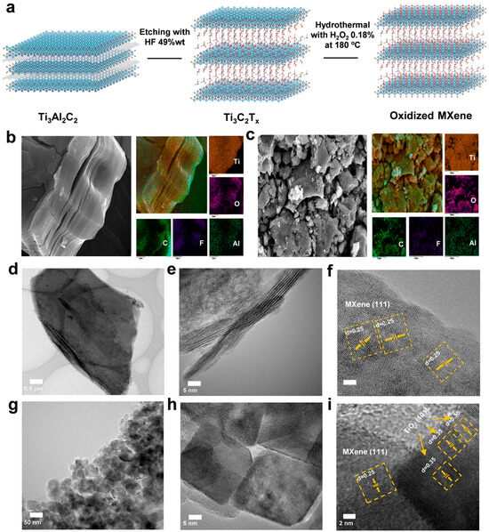
Figure 7.
(a) Schematic illustration of the synthesis of MXene from the MAX phase followed by hydrothermal oxidation to obtain oxidised MXene. (b) Scanning electron microscopy (SEM) image and energy-dispersive X-ray spectroscopy (EDS) elemental mapping of pristine MXene. (c) SEM image and EDS elemental mapping of oxidised MXene. Microstructural characterisation of pristine and oxidised MXene. (d,g) Field-emission transmission electron microscopy (FE-TEM) images, (e,h) magnified TEM images, and (f,i) high-resolution TEM (HR-TEM) images. Reprinted from Ref. [25] Copyright 2025 Somnath S. Kundale et al.
2.4.2. Edge Modification and Antioxidation
Wang et al. delineated a method for passivating the edges of MXenes with organic compounds or polymers to tackle the problem of long-term stability [26]. For example, the incorporation of positively charged polyelectrolytes or the application of antioxidants (such as ascorbic acid) can effectively inhibit water molecules from interacting with the Ti atoms at the edges, consequently prolonging the storage lifespan of the devices to several months or even years while preserving their memristive functionality.
2.5. Doping
Compounding MXenes with other functional materials has emerged as a prevalent strategy to alleviate the performance bottleneck of single-component materials. Doping imparts multi-functional qualities to materials, hence improving their performance in composite applications.
2.5.1. Metal Nanoparticle Doping
Both Wang et al. and Teixeira et al. noted the incorporation of Ag, Pt, or Au nanoparticles within or on the surface of MXene layers. These metallic nanoparticles function as Electric Field Concentrators, resulting in the amplification of localised electric fields. This markedly diminishes the randomness of conductive filament generation, hence substantially enhancing device-to-device (D2D) and cycle-to-cycle (C2C) consistency, as well as the stability of the devices. For example, Ag-doped MXene devices can attain switching properties without undergoing a forming procedure.
2.5.2. Nitrogen Doping and Wrinkled Structure
Nitrogen-doped wrinkled MXenes can be synthesised using the melamine-formaldehyde (MF) template technique. The wrinkled architecture inhibits the restacking of MXene nanosheets and preserves a high specific surface area. The incorporation of nitrogen atoms modifies the electron cloud distribution and increases the adsorption sensitivity to neurotransmitters (e.g., acetylcholine), which is essential for developing biocompatible brain interfaces [26].
2.6. Correspondence Between Synthesis Strategies, Microstructures and Physical Mechanisms
The effects of different treatment strategies on electron and ion transport, along with their dominant physical mechanisms, are summarized in Table 1.

Table 1.
Effects of Different Treatment Strategies on Electrons/Ions.
3. Resistive Switching Mechanisms and Physical Models
Comprehending the microscopic operational mechanism of MXene-based memristors is essential for optimising device performance and customising neuromorphic functions. In contrast to conventional metal oxide memristors, the distinctive two-dimensional layered architecture of MXene, along with its adjustable metal-semiconductor-insulator electrical properties and abundant surface chemical environment, imparts varied and hybrid characteristics to its resistive switching mechanisms, as summarized in Table 2.
Table 2.
Comparison of Key Electrical Performance Parameters of Different MXene-based Memristors.
3.1. Electrochemical Metallization Mechanism (ECM)
The Electrochemical Metallisation Mechanism (ECM), sometimes referred to as Conductive Bridge Random Access Memory (CBRAM), is the predominant mechanism in MXene-based memristors, particularly in devices utilising active metals (e.g., Ag, Cu) as the upper electrode.
Under forward bias, the active electrode (using Ag as an example) experiences oxidation, resulting in the formation of metal cations (Ag→Ag+ + e−) (Figure 8). Propelled by the electric field, these cations traverse the MXene insulating/semiconducting layer, subsequently undergoing reduction and deposition at the inert bottom electrode (e.g., Pt, Au, ITO). A continuous metallic conductive filament is ultimately formed, transitioning the device from the High Resistance State (HRS) to the Low Resistance State (LRS). In a reverse bias, the conductive filament disintegrates and breaks, restoring the device to its initial state.
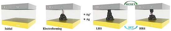
Figure 8.
Schematic diagram illustrating the Electrochemical Metallization (ECM) mechanism within a vertical Ag/Ti3C2Tx/Au memristor. (I) The initial state of the device with an insulating MXene layer and no conductive path. (II) The electroforming process, where the active Ag top electrode is oxidized to generate Ag+ ions that migrate through the MXene layer and nucleate at the bottom electrode. (III) The Low Resistance State (LRS) is achieved during the SET process once the accumulated Ag atoms form a continuous conductive filament bridging the two electrodes. (IV) The High Resistance State (HRS) is restored during the RESET process when the conductive filament ruptures under a reverse bias. Reprinted from Ref. [26] Copyright 2025 Wang, K. et al.
Wang et al. indicated that MXene functions not only as a basic solid electrolyte in the ECM mechanism; its structural properties significantly impact the development of conductive filaments [26]. The numerous electronegative functional groups (notably -F and -O) on the MXene surface can establish electrostatic contacts with metal cations (e.g., Ag+). These functional groups act as “binding sites” for ion hopping, directing cations to travel along the edges or interlayer gaps of MXene nanosheets, thus mitigating the unpredictability of conductive filament production. Moreover, titanium vacancies created during the etching process are deep-level imperfections that can efficiently capture metal ions and serve as nucleation sites for the development of conductive filaments. The pre-established nucleation sites markedly decrease the device’s forming voltage.
3.2. Valence Change Mechanism (VCM)
The Valence Change Mechanism (VCM) is fundamentally based on the movement of anions, predominantly oxygen ions (O2−), and the creation of conductive pathways formed by oxygen vacancies (VO). This behaviour is most evident in MXene devices undergoing oxidation treatment.
Kundale et al. [25] demonstrate that the in situ synthesised TiO2 nanocrystal layer on the Ti3C2Tx surface, produced using a hydrothermal process, functions as the central region for the VCM mechanism.
- SET Procedure
The SET process pertains to the creation of conductive channels by oxygen vacancies. Imposing a forward electric field generates a potential difference; the electric field force influences O2− within the TiO2 lattice, prompting their detachment from lattice sites and migration towards the cathode or capture by functional groups on the MXene surface. Positively charged oxygen vacancies (VO) remain in the lattice following the removal of O2−. The sustained application of the electric field results in a progressive increase in the concentration of oxygen vacancies. Upon reaching the percolation threshold of oxygen vacancy concentration—wherein the vacancies are adequate to establish a continuous “pathway” between the anode and cathode—electrons are swiftly conducted through these oxygen vacancies. Ultimately, the device resistance decreases significantly, transitioning from the High Resistance State (HRS) to the Low Resistance State (LRS), so finalising the “writing” operation.
- 2.
- RESET Procedure
The RESET process is the inverse of the SET process. An opposing electric field propels oxygen ions to replenish the vacancies. As numerous oxygen vacancies are replenished, the previously continuous conductive pathways are disrupted, impeding electron transport and causing the device resistance to revert to the high resistance state, so accomplishing the “erasing” operation.
X-ray Photoelectron Spectroscopy (XPS) is an essential method for validating the VCM mechanism. Yan et al. determined that the reduction of Ti4+ to Ti3+ is commonly observed in the LRS, correlating with a decrease in oxygen content and an increase in oxygen vacancy concentration [27]. Redox processes predominantly transpire at the peripheries of MXene or the interface of the oxide layer.
3.3. Charge Trapping and Quantum Well Effect
Not all resistive switching entails the physical migration of atoms. In certain high-performance and high-stability MXene devices, electron transport within the band structure predominates the resistive switching behaviour.
The I-V characteristics of numerous MXene/polymer or MXene/oxide composite devices adhere to the Space-Charge-Limited Current (SCLC) concept. Defect energy levels are present inside the materials, and the processes of carrier injection and transport are governed by these flaws and the space-charge effect. As illustrated in Figure 9, the conduction mechanism of fully etched MXene (f-Ti3C2Tx) is primarily dominated by charge trapping and de-trapping processes. Injected electrons are captured by defect sites within the MXene layers, which severely restricts current flow until all traps are filled, aligning with the SCLC model.The space-charge-limited current model typically comprises three distinct areas, each characterised by specific properties and underlying physical mechanisms, as detailed in Table 3 below.
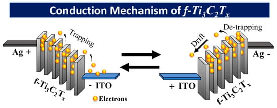
Figure 9.
Schematic diagram of the composition mechanism of fully etched (f-Ti3C2Tx). Reproduced with permission from [24]. Copyright 2024, American Chemical Society.
Table 3.
Core Characteristics and Corresponding Physical Mechanisms of the Space-Charge-Limited Current Model.
Gosai et al. developed a novel physical model in their research on partially etched MXene (p-Ti3C2Tx) [24]. The leftover Al ion pillars and DMSO molecules in p-Ti3C2Tx increase the interlayer gap, creating alternate conductive layers (MXene nanosheets) and insulating barrier layers (Al/DMSO layers). This configuration appears as a sequence of quantum wells in the band diagram. Electrons are restricted within the quantum wells, unable to traverse the barriers, leading to diminished electrical conductivity. When the applied voltage surpasses the threshold (~1 V), electrons gain the energy to traverse the barriers through tunnelling or thermal emission, or engage in defect-assisted transport facilitated by defects within the barrier layers, resulting in a sudden increase in current. Research has demonstrated that the fabrication of van der Waals heterojunctions between MXene and other two-dimensional materials can efficiently alter the contact type and Schottky barrier height. This theoretically substantiates the viability of artificially constructing tunable barriers via structural design [29]. Theoretical investigations of Ti3C2O2 quantum dots have demonstrated that reducing the size of MXene to the zero-dimensional scale results in a pronounced quantum confinement effect, causing substantial alterations in its electrical structure and optical characteristics. This indirectly confirms that electron behaviours can be efficiently controlled in dimensionally constrained devices [30]. In contrast to the significant atomic rearrangement involved in the ECM method, this switching mechanism, reliant on the electronic band structure, allows Gosai’s devices to demonstrate remarkable mechanical stability and cycling longevity exceeding 10,000 cycles.
3.4. Schottky Barrier Modulation
The modulation of interfacial barriers is the crucial technique for achieving the integration of sensing and memory in devices equipped with sensing, memory, and computational functions.
Kundale et al. [25] discovered that the resistive switching behaviour of the Au/Oxidised-MXene/Au device is influenced by both voltage and the surrounding atmosphere. The oxidised MXene displays n-type semiconductor properties, creating a Schottky barrier upon contact with the Au electrode. Upon the adsorption of oxidising gases (e.g., NO2), gas molecules extract electrons from MXene, resulting in the expansion of the depletion layer, the rise in the Schottky barrier, and the augmentation of device resistance (suppression of synaptic weight) [25,31,32]. The adsorption of reducing gases (e.g., NH3) or CO2 under particular conditions (dependent on surface adsorption configuration) alters carrier concentration, leading to a drop in barrier height and a decrease in resistance, hence enhancing synaptic weight. Research has demonstrated that the combination of noble metals (e.g., Au) and MXene can create heterojunctions, whose interfacial barriers are responsive to gases and are crucial for signal amplification [33]. This technique enables chemical compounds to function as “gate” signals for the regulation of memristor synaptic weight, accurately mimicking the depolarisation and hyperpolarisation processes of real olfactory neurones.
Teixeira et al. noted that the integration of MXene with ferroelectric materials (e.g., HfZrO, BFO) can modify the direction of band bending on the MXene surface by the reversal of ferroelectric polarisation, thereby achieving non-volatile resistive switching. This is an entirely electronic switching apparatus with exceptional speed. The resistive switching mechanism in the Cu/Ti3C2/BaFe12O19/Pt memristor is attributed to the combined effects of barrier alterations induced by ferroelectric polarisation and oxygen vacancies. This behaviour corresponds with the ‘dual-regulation process’ recently documented by Yue et al., wherein ‘oxygen vacancy redistribution and ferroelectric polarisation dynamically govern the parameters of the Schottky barrier.’ [34]. This device exhibits a significant switching ratio, minimal operating voltage, and reliable multi-level storage capacity, successfully simulating several forms of synaptic plasticity. A separate study involved the integration of ferroelectric MXene (Ti3C2Tx) with the traditional ferroelectric material BiFeO3 (BFO) to construct a flexible memristor. The research indicated that the incorporation of MXene enhances the interface and promotes resistive switching behaviour, while the device demonstrates intricate functionalities like multi-level storage and negative differential resistance [35].
3.5. Mixed Mechanism
In practical application, a singular mechanism often fails to account for all phenomena. Gosai et al. and Wang et al. both underscored the presence of the “mixed mechanism” [24,26]. In Gosai’s p-Ti3C2Tx device, researchers noted that trap-assisted electron tunnelling and quantum well hopping predominated as the primary processes at low voltages. Conversely, with elevated voltages or extended electrical stress, the migration of Ag+ ions may commence, resulting in the creation of weak conductive filaments. This hybrid mechanism explains the device’s capability to demonstrate both analogue slow resistive switching, appropriate for synaptic simulation, and digital switching behaviour, suited for data storage, facilitating the transition between both modes through modulation of the compliance current.
The physical mechanisms of MXene-based memristors encompass a diverse spectrum, from atomic-scale migration to electronic-scale transformation. ECM and VCM systems provide elevated switching ratios and non-volatility, rendering them appropriate for high-density data storage. The charge trapping and quantum well methods, such as those in p-Ti3C2Tx, provide exceptional homogeneity and little power consumption, which are advantageous for high-precision neuromorphic computing [24]. Simultaneously, Schottky barrier modulation offers a physical interface for the integration of environmental sensing, such as gas sensors, and memory functions [25].
A comprehensive understanding and disaggregation of these mechanisms will establish the theoretical foundation for the future design of MXene-based devices with customised functionality (e.g., ultra-low power consumption or multimodal sensing).
4. Implementation of Neuromorphic Computing Functions
The fundamental objective of neuromorphic computing is to develop hardware systems that exhibit efficiency, fault tolerance, and adaptive learning capabilities comparable to those of the human brain. The basis for attaining this objective resides in the construction of artificial synapses. Biological synapses adjust the connection strength between two neurones (i.e., synaptic weight) by controlling the quantity of neurotransmitter release and the sensitivity of receptors. In electronic engineering, the conductance value (G) of a memristor is closely correlated with the synaptic weight (W). This chapter will comprehensively examine recent advancements in MXene-based memristors for emulating biological synaptic functions, concentrating on the evaluation of the physical realisation of short-term and long-term plasticity, Hebbian learning principles, and the pattern recognition efficacy in artificial and spiking neural network simulations.
4.1. Basic Simulation of Synaptic Plasticity
Teixeira et al. define synaptic plasticity as comprising two categories based on temporal scale: Short-Term Plasticity (STP) and Long-Term Plasticity (LTP) [36]. Due to its distinctive ion-electron hybrid conduction mechanism, the MXene device can effectively include these two time frames [37].
4.1.1. Short-Term Plasticity (STP) and Paired-Pulse Facilitation (PPF)
Short-term synaptic plasticity functions as the physiological foundation for temporal information encoding and high-pass filtering in biological brain systems [38]. Paired-pulse facilitation (PPF) is characterised by the phenomenon in which two consecutive pulses, separated by a time interval of Δt, stimulate the presynaptic membrane, resulting in a greater amplitude of the postsynaptic current induced by the second pulse compared to the first. It is acknowledged as a principal manifestation of short-term plasticity (STP) [38]. This dynamic attribute is essential for the temporal processing of brain impulses and the filtration of signals at specific frequencies.
In MXene-based memristive devices, PPF properties have been effectively replicated and thoroughly measured. Research has shown that the PPF index displays an exponential decay pattern as the pulse interval Δt increases, and this decay can be precisely characterised by a double-exponential function comprising fast and slow components [39]. This mathematical relationship closely aligns with the behaviours of biological synapses. The PPF behaviour in MXene devices mostly arises from the partial relaxation of conductive filaments or the charge trapping effect. The movement of metal ions caused by the initial electrical pulse or the injected charge carriers (e.g., electrons) does not entirely dissipate during the pulse duration. Thus, upon the arrival of the second pulse, the device exhibits an elevated baseline conductance, leading to an amplified current response.
The PPF features of MXene devices confer upon them intrinsic use in processing dynamic time-series data, including speech recognition and Morse code decoding. The exponential decay filtering characteristic resembles the response function of a Butterworth high-pass filter, indicating that MXene-based artificial synapses may efficiently eliminate low-frequency noise and enhance signal edges. Consequently, they exhibit immediate applicability in neuromorphic perception systems, including tactile sensing [40] and picture edge enhancement [41].
4.1.2. Long-Term Plasticity (LTP/LTD) and Weight Update
Long-Term Potentiation (LTP) and Long-Term Depression (LTD) are fundamental mechanisms of memory formation and neural network learning. Wang et al. summarised the capacity of MXene devices to continuously modulate conductance by applying a sequence of successive positive and negative pulses. An optimal LTP/LTD curve must have superior linearity and symmetry. Traditional filamentary memristors (e.g., Ag/oxide-based devices) typically experience a sudden SET process followed by a slow RESET phase, leading to considerable asymmetry. Conversely, the partially etched p-Ti3C2Tx device created by Gosai et al. exhibits remarkable linearity under both identical and nonidentical pulse schemes (Figure 10a,b). This advantage is ascribed to its “quantum well” mechanism, which limits the sudden increase in current and facilitates a more regulated creation and dissolution of conductive channels. This feature is essential for enhancing the training accuracy of neural networks. Figure 10c clearly demonstrates the primary purpose of artificial synapses in emulating the “potentiable and depressible” attributes of biological synapses, together with their nonlinear and asymmetric plasticity characteristics. To quantify this behaviour, the conductance (G) and pulse number (P) are used to calculate the nonlinearity parameter.
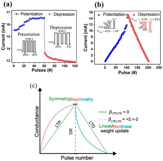
Figure 10.
(a) Identical pulse. (b) Nonidentical pulse. Reproduced with permission from [24]. Copyright 2024, American Chemical Society. (c) Relationship between conductance update and its nonlinearity and asymmetry. Reprinted from Ref. [18] Copyright 2016 Zhang, T. et al.
In Equations (4) and (5), , β gives the linearity, Gmax/Gmin are the maximum/minimum conductance values, and P is the normalised pulse number [15].
4.2. Hebbian Learning Rule and STDP
The principle that neurones that activate simultaneously will have their connections reinforced is fundamental to Hebbian learning theory. Spike-Timing-Dependent Plasticity (STDP) serves as its quantitative biological principle.
Physical Implementation of STDP
Spike-Timing-Dependent Plasticity (STDP) is a fundamental bio-inspired learning principle in neuromorphic computing. This rule delineates that the alteration in weight (Δw) of a synaptic connection—typically denoted by the conductance of an artificial synaptic apparatus—hinges on the temporal disparity (Δt = tpost − tpre) between the presynaptic spike (tpre) and the postsynaptic spike (tpost) [42]. The mathematical expression and physical significance are as follows: when Δt > 0, meaning the presynaptic neurone activates before the postsynaptic neurone, the synaptic weight is enhanced (Δw > 0), reflecting the causal relationship in neural activities and forming the foundation for Long-Term Potentiation (LTP). Conversely, when Δt < 0, the synaptic weight is diminished (Δw < 0), indicative of Long-Term Depression (LTD) [42]. This weight updating mechanism, predicated on the relative timing of spikes, underpins the execution of sophisticated cognitive functions, including unsupervised learning and pattern recognition.
The simulation of STDP behaviour via MXene-based memristive devices has emerged as a leading area of research. Researchers have effectively replicated the traditional antisymmetric STDP curve [15] by engineering particular voltage pulse sequences (e.g., superimposed rectangular or triangular waves) to serve as pre- and postsynaptic spikes, which were subsequently applied to the device. Experimental data demonstrate that the correlation between weight change Δw and spike timing difference Δt can be precisely modelled by the exponential decay function Δw = Aexp(−Δt/τ), aligning closely with the STDP model of biological synapses. Distinct STDP behaviours have been found in MXene-based stacked devices with varying architectures, where the maximum weight change rate (Max Δw) and the requisite pulse amplitude differ according to the specific device architecture.
Notably, STDP does not exist in a singular, fixed form. By meticulously controlling the internal physical mechanisms of the device (e.g., integrating ferroelectric polarisation switching with oxygen vacancy migration) or altering the configuration of external stimulus pulses, a symmetric STDP learning window can be attained [43]. The “symmetric Hebbian learning” rule is essential for developing associative memory networks; for instance, in Hopfield-type recurrent networks, it can significantly improve the network’s pattern recognition and recall capacities in noisy conditions [44].
4.3. Neural Network Simulation and Pattern Recognition
To assess the viability of MXene devices in actual AI applications, researchers typically use artificial neural networks (ANNs) for software simulation utilising device parameters obtained from studies (e.g., nonlinearity α, dynamic range Gmax/Gmin, and cycle consistency σ).
4.3.1. MNIST Handwritten Digit Recognition
In neuromorphic computing, handwritten digit recognition tasks, exemplified by the classification of the MNIST dataset, are frequently considered a “fruit fly”-style benchmark for assessing the efficacy of novel artificial synaptic devices, due to their established datasets and standardised network architectures [26]. These tests can accurately measure the ability of devices to replicate the fundamental function of biological synapses, specifically plasticity, and forecast their potential in more intricate brain networks.
Networks intended for these benchmark evaluations generally utilise a conventional multi-layer perceptron (MLP) architecture. A example study utilised a configuration with 784 input neurones (representing 28 × 28 pixel images), one hidden layer with 250 nodes, a second hidden layer with 125 nodes, and 10 output neurones (representing digits 0–9) [26]. The training procedure utilises the error backpropagation algorithm, which fundamentally involves the precise correlation of the theoretical weight updates computed by the algorithm with the conductance alterations of physical devices (e.g., memristors). The correlation between software algorithms and hardware responses is the primary criterion for evaluating the appropriateness of devices for compute-in-memory architectures.
MXene-based synaptic devices have exhibited exceptional performance in benchmark evaluations, primarily evident in three major aspects:
- Systems utilising MXene materials, such as Ti3C2Tx, can attain around 95% accuracy in MNIST classification tasks [45];
- Superior device linearity promotes swift network convergence. A study indicated that its MXene array could achieve nearly flawless pattern training accuracy after just 9 training epochs [46];
- Device homogeneity is essential for array applications. Research indicates that memory devices utilising MXene-TiO2 Schottky junctions demonstrate superior device-to-device repeatability [47].
4.3.2. Fashion-MNIST
Kundale et al. advanced beyond basic digits to tackle the more intricate Fashion-MNIST dataset, which consists of greyscale images of apparel, footwear, accessories, and other things, as depicted in panels c and d of Figure 11 below. Kundale utilised the response of oxidised MXene to CO2 gas to achieve multi-level weight states regulated by gas concentration. The results attained an accuracy of 82% in the Fashion-MNIST challenge. Despite this value being inferior to the state-of-the-art performance achievable by pure software algorithms on the same dataset (e.g., specific deep convolutional networks can surpass 99%) [48], its pivotal importance resides in the inaugural experimental confirmation of the viability of directly modulating the learning process of hardware neural networks through external chemical environmental signals. This study illustrates the applicability of MXene-based devices in intricate perceptual computing tasks and, more significantly, establishes a novel trajectory for the advancement of next-generation neuromorphic systems with environment-adaptive learning capabilities—specifically, a new category of intelligent hardware capable of directly perceiving and integrating chemical information for computation, akin to the biological olfactory system.
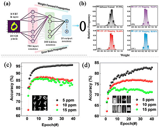
Figure 11.
(a) Schematic of a three-layer fully connected ANN with 784 input neurons, 300 hidden layer neurons, and 10 output neurons. (b) Weight distribution, recognition accuracy. Reprinted from Ref. [26] Copyright 2025 Wang, K. et al. (c) Classification accuracy of simulated ANN models based on the synaptic behaviour of the device under different CO2 concentrations for the digit MNIST dataset. (d) Classification accuracy of simulated ANN models based on the synaptic behaviour of the device under vacuum and different CO2 concentrations for the fashion-MNIST dataset. Reprinted from Ref. [25] Copyright 2025 Somnath S. Kundale et al.
4.4. Associative Memory and Pavlovian Experiments
Alongside their exceptional performance in supervised learning (e.g., image classification), MXene-based neuromorphic devices demonstrate distinctive potential for executing unsupervised associative learning, resembling biological instincts, with the simulation of classic Pavlovian conditioning serving as the most illustrative example [49]. This experiment is considered a significant advancement in the development of hardware with adaptive learning capabilities.
This experiment has confirmed the establishment of associative memory in hardware by emulating the renowned behavioural paradigm of “Pavlov’s dogs.” The essence resides in using the property of MXene devices, wherein their conductance, indicative of synaptic weight, may be altered by training history [50]. The behavioural benchmark assessments are displayed in Table 4 below.
Table 4.
Behavioural Paradigm of “Pavlov’s Dogs”.
This learning behaviour has been empirically validated in multiple MXene devices. Research has confirmed that Ti3C2Tx MXene memristors can function as monolithic devices to exemplify classical conditioning learning [49]. Moreover, flexible MXene floating-gate synaptic transistors can replicate Pavlovian training in response to external stimuli, demonstrating its promise in cognitive learning [51]. A further study has utilised the photoelectric response properties of MXene to replicate the modelling of Pavlovian conditioning for associative learning [52].
The above experiments demonstrate that MXene-based memristors provide significant potential for simulating synaptic plasticity, implementing learning rules, and constructing associative memory. Zhang et al. concentrated on the collaborative design of multifunctional reconfigurable devices and compute-in-memory integrated architectures to enhance the progression of neuromorphic computing from individual devices to system integration [53]. The researchers constructed ferroelectric memristors featuring a Cu/Ti3C2/BaFe12O19 architecture, achieving dual-mode reconfigurable operations of threshold switching and resistive switching within the same device by modulating the compliance current, thereby fulfilling the functional requirements of both dynamic synapses and non-volatile memory on a single hardware platform. This device effectively replicated comprehensive biological synaptic functions, encompassing short- and long-term plasticity, paired-pulse facilitation, and spike-timing-dependent plasticity. A convolutional neural network was developed, attaining an 85% accuracy in online learning for the CIFAR-10 image classification test [53]. Simultaneously, its non-volatile resistive switching property was employed for circuit-level logic operations, achieving AND and OR gates as well as 1-bit adder functions, thus showcasing multi-task processing capabilities in compute-in-memory systems. This study offers a viable technical pathway for the advancement of low-power (<1 V), highly compatible, and versatile neuromorphic computing hardware from the viewpoints of device physics and system applications. It also reflects and enhances the design concept of MXene-based devices within integrated systems of complex perception, computation, and storage.
As summarized in Table 5, this chapter illustrates the comprehensive capabilities of MXene-based memristors in neuromorphic computing. At the physical level, they can precisely replicate diverse plasticity rules of biological synapses (STP, LTP, STDP, PPF); at the algorithmic level, leveraging their superior linearity and low-power attributes, they attain an accuracy near the theoretical maximum (~95%) in standard tasks such as handwritten digit recognition; at the system level, they demonstrate the ability to manage intricate patterns (Fashion-MNIST) and associative memory.
Table 5.
Implementation of Neuromorphic Computing Functions Based on MXene-Based Devices.
5. Multifunctionality and Cutting-Edge Applications: Toward Integration of Sensing, Memory and Computing
The proliferation of edge devices for the Internet of Things (IoT) presents significant bandwidth limitations and energy consumption difficulties when delivering large analogue signals collected by sensors to the cloud or central processing units (CPUs) for processing. The amalgamation of sensing, memory, and computing necessitates equipping sensors with “memory” and “computing” functionalities to perform preprocessing and feature extraction directly at the signal acquisition stage.
Leveraging their distinctive surface chemical sensitivity, photoelectric response properties, and mechanical flexibility, MXene materials have emerged as an optimal foundation for the development of multimodal neuromorphic systems. This chapter will methodically discuss the innovative applications of MXenes in flexible tactile sensing, artificial olfactory sensing, and nociceptive perception.
5.1. Flexible Wearable Electronics and Mechanical Sensing
Flexible neuromorphic devices are essential components for the development of electronic skin (E-Skin) and soft robotics. The stratified architecture of MXene provides it with an intrinsic ability to dissipate stress during flexion; nonetheless, preserving the stability of memristive performance under significant strain is a considerable difficulty.
5.1.1. Structural Engineering and Mechanical Stability
The flexible MXene memristive device demonstrated outstanding performance in mechanical and environmental reliability tests. Systematic limit tests indicated that the device could sustain typical SET/RESET resistive switching capability even at a bending angle of up to 73° (Figure 12a). Subsequent mechanical durability assessments indicated that during 1000 continuous bending cycles at a 73° angle, no notable deterioration was detected in its critical switching parameters (Figure 12b), which included a set voltage of around 1 V and a high/low resistance state ratio of up to 103 [24]. The device successfully maintained its short-term synaptic plasticity, as the paired-pulse facilitation (PPF) index exhibited highly consistent decay behaviors under both flat and curved conditions (Figure 12c). Moreover, due to the efficient encapsulation with PET materials, the device demonstrated exceptional electrical resilience across a relative humidity spectrum of 40% to 70% and a temperature range of 25 °C to 80 °C. These results collectively affirm that the device structure exhibits strong stability to endure severe mechanical deformation and fluctuating environmental conditions.
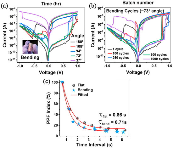
Figure 12.
(a,b) curves at different bending angles and bending cycle test data (c) Synaptic plasticity testing under curved conditions. Reproduced with permission from [24]. Copyright 2024, American Chemical Society.
This research developed a stacked device architecture comprising PET/ITO/p-Ti3C2Tx/Ag. Within this structure, the partially etched p-Ti3C2Tx served a pivotal function: the remnant aluminium atomic pillars functioned as structural supports, securely linking adjacent MXene nanosheets and significantly improving the interlayer adhesion of the two-dimensional material. This distinctive structure can markedly inhibit interlayer slippage or delamination that may arise after repetitive bending, so establishing the basis for the device’s mechanical stability.
5.1.2. Tactile Memory Function
Researchers have recreated the “adaptability” of touch perception based on the aforementioned flexible gadgets. For example, piezoelectric materials (such as PVDF) or triboelectric nanogenerators (TENG) are employed to transform pressure signals into voltage pulses for operating MXene memristors. As the frequency of pressure stimulation escalates, the device’s conductance progressively increases, emulating the cumulative effect and short-term memory of the skin in reaction to pressure signals.
5.2. Chemically Reconfigurable Memristors and Artificial Olfaction
The biological olfactory system is capable of detecting gases as well as memorising and categorising odours (e.g., the perception of a specific scent evokes memories). Conventional metal oxide gas sensors (e.g., SnO2) often possess solely a sensing capability and experience elevated operating temperatures and prolonged recovery durations. Kundale et al. created innovative “chemically reconfigurable” memristors utilising oxidised MXene [25].
5.2.1. Gas-Sensing–Memristive Coupling Mechanism
The operational principle of the Au/Oxidised-MXene/Au memristor fundamentally depends on the reversible physicochemical manipulation of the Schottky barrier at the MXene surface by surrounding gas molecules [25]. Upon exposure to gases with varying characteristics, gas molecules experience adsorption and charge transfer on the MXene surface. Upon exposure to oxidising gases (e.g., NO2), NO2 molecules function as electron acceptors, removing electrons from the MXene surface. This results in a reduction of majority carriers (electrons) in n-type MXene, an expansion of the depletion layer, an increase in the Schottky barrier, and a rise in the overall resistance of the device, emulating long-term depression (LTD) behaviour. Simultaneously, when exposed to reducing gases, these gases function as electron donors, transferring electrons to the MXene surface. This elevates the carrier concentration, diminishes the depletion layer, decreases the Schottky barrier, and mitigates the device resistance, so emulating long-term potentiation (LTP) behaviour.
Gas adsorption is a dynamic equilibrium process in which the partial pressure of the gas immediately influences the quantity of molecules adsorbed on the MXene surface, hence accurately controlling the overall amount of transferred charge. Consequently, by regulating the gas concentration in the environment (e.g., accurately adjusting NO2 to varying levels such as 5, 10, 15 ppm), the Schottky barrier of the device can be constantly and reversibly adjusted to a range of various steady-state heights. This immediately relates to a series of distinct and stable device resistance (conductance) states, facilitating multilevel non-volatile memory that is programmed externally by chemical signals. Each gas concentration corresponds to a distinct “weight” condition, accurately reflecting the property that biological synaptic weights are influenced by the chemical environment.
5.2.2. Olfactory Synaptic Function Demonstration
MXene-based neuromorphic devices possess distinctive capabilities in emulating the biological olfactory system, with their primary advantage being the direct conversion of chemical gas signals into programmable non-volatile conductance states, facilitating the perception, memory, and adaptive processing of odour information [54].
A fundamental characteristic of the devices is their sensitivity to pure gas pulses. Upon exposure to particular gases (e.g., CO2 NO2), gas molecules engage in charge transfer with the MXene surface, thereby immediately altering its conductance (Figure 13); subsequent to the removal of the gas, this conductance state might persist for many seconds to hours, effectively creating a “memory” of gas exposure events. This chemically induced non-volatile resistive switching obviates the dependence on conventional electrical pulse programming, establishing a hardware basis for the direct recording of chemical information. Research has validated that the “gas memristor” utilising V2CTx can react to SO2 gas in milliseconds and maintain its conductance state, exemplifying the capability of gas pulse memory [55].
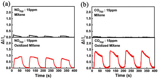
Figure 13.
(a) NO2 response; (b) CO2 response. Reprinted from Ref. [25] Copyright 2025 Somnath S. Kundale et al.
The gadgets facilitate the synergistic regulation of synaptic weights by electrical stimuli (voltage pulses) and chemical stimuli (gas concentrations). Voltage pulses provide rapid and accurate incremental modifications of conductance, but the gaseous environment can universally alter the conductance baseline of the devices. This dual-modulation capacity enables the devices to concurrently process spatiotemporal electrical signals and chemical concentration gradients, establishing a physical basis for the development of multimodal perception-computation integrated systems. The synaptic plasticity of memristors made from oxidised MXene and ZrO2 quantum dots may be efficiently regulated by the external chemical environment, illustrating the potential for electrical-chemical synergy [56].
In functional verification, the Fashion-MNIST and Digit-MNIST datasets were utilised as benchmark tasks. Incorporating gas concentration as an extra input parameter (simulating environmental interference), the developed hardware neural network sustained an identification accuracy of 82–95% despite gas changes. This signifies that the system may flexibly modify its computational techniques based on the surrounding chemical context, similar to the resilient detection capabilities of the biological olfactory system in intricate odour situations. This confirms the applicability of MXene devices in environment-adaptive neuromorphic computing, offering guidance for the advancement of next-generation intelligent sensing-computation integrated systems [54].
5.3. Nociceptive Perception and Nociceptors
The sense of pain is an essential mechanism for organisms to safeguard themselves against harm. Artificial nociceptors must exhibit threshold characteristics, lack flexibility, and incorporate sensitisation traits [57,58].
5.3.1. Threshold Switching Characteristics
Huang et al. [59] indicate that specific MXene-based memristors, particularly those utilising Ag diffusion in TS devices, demonstrate volatile threshold switching properties. The device will only initiate an action potential (SET) when external stimuli (voltage, pressure, temperature) surpass a designated threshold. This emulates the “all-or-none” paradigm of biological nociceptive neurones. Upon the cessation of the stimulus, the conductive filaments spontaneously fracture, causing the device to return to a high-resistance state, so emulating the attenuation of pain perception.
5.3.2. Sensitization and Hyperalgesia
To replicate the advanced self-defence mechanisms of biological nervous systems, MXene-based memristors can be enhanced with the dynamic learning ability associated with hyperalgesia. Research indicates that the application of prolonged heat impacts or electrical stress preconditioning to these devices can efficiently alter and lower the triggering threshold of their resistive switching [60]. This process emulates the physiological phenomena of “hyperalgesia” in biological tissues, when nociceptors demonstrate excessively heightened responses to stimuli that are typically innocuous following injury. The fundamental physical mechanism is that external energy input (e.g., heat or electricity) can modify the kinetic processes of conductive filament formation or the interfacial barrier within the device, thus facilitating the generation of action potential-like signals at reduced voltages upon subsequent stimulation [61]. Bionic devices equipped with adaptive threshold modulation capabilities are crucial for developing feedback protection networks in intelligent prosthetics and robotic systems. They enable dynamic adjustments in sensitivity to potential hazard signals based on “injury” history, akin to living organisms, thereby facilitating enhanced environmental interaction and self-protection [62].
5.4. Near-Sensor Computing
To achieve a highly energy-efficient and low-latency neuromorphic sensing system, an effective approach is the heterogeneous integration of MXene memristor arrays at the backend of sensor chips [63]. This “near-sensor” or “in-sensor memory computing” architecture significantly reduces the transmission distance of raw analogue signals and can entirely circumvent the energy-consuming analogue-to-digital conversion (ADC) process, facilitating direct information processing and feature extraction in the analogue domain [63]. Due to its superior electrical conductivity, mechanical flexibility, and solution-processable properties, MXene has become an exemplary contender for actualising this concept. Research has shown that optimising semiconductor-compatible processes such as centrifugation, spin-coating, photolithography, and dry etching enables high-resolution and high-performance MXene patterning at the wafer scale, facilitating monolithic integration with silicon-based CMOS sensors (e.g., image or pressure sensor arrays) [64]. This comprehensive integration strategy markedly decreases system power usage and latency, establishing a vital technical framework for the advancement of next-generation intelligent edge-sensing devices.
The emergence of MXene materials is propelling the advancement of neuromorphic devices from individual “electronic synapses” to “multimodal intelligent units”. In practical applications, flexible devices (Gosai et al.) have resolved the mechanical compatibility challenges of wearable electronics; chemically reconfigurable memristors (Kundale et al.) have introduced a novel approach for intelligent olfaction; and nociceptive devices (Huang et al., Wang et al.) have broadened the sensory capabilities of robots.
This trend of integrating sensing, memory, and computing significantly reduces power consumption and latency in edge computing devices, while also establishing a hardware foundation for developing brain-inspired intelligent systems with autonomous sensing and decision-making abilities.
5.5. Comparative Analysis: MXenes vs. Other 2D Neuromorphic Materials
To thoroughly assess the capabilities of MXenes, it is crucial to compare them with other prominent two-dimensional (2D) neuromorphic materials, including Transition Metal Dichalcogenides (TMDs), Graphene, and hexagonal Boron Nitride (h-BN). Table 6 summarises the key indicators from relevant research papers.
Table 6.
Benchmark Comparison of MXene-based Memristors against Leading 2D Material Synaptic Devices.
MXene-based memristors generally exhibit extremely low working voltages (<1 V) due to their elevated intrinsic conductivity and minimal ion migration barriers. Conversely, grain-boundary mediated MoS2 memristors generally necessitate elevated set fields (about 8.3 V) to facilitate dopant migration, although providing distinctive gate-tunability rarely observed in two-terminal MXene devices [65] Phase-change MoTe2 devices use an electric-field-induced transition between the semiconducting 2H and metallic Td phases, facilitating switching at moderate voltages (about 2.3 V) with remarkable speed (less than 10 ns) [66].
Linearity in synaptic weight modifications is essential for the precision of neural network training. Recently, h-BN memristors have attained very linear and symmetric analogue switching by constraining numerous nano-filaments with GaN nano-cones, resulting in a classification accuracy of 96.2% in MNIST simulations [67]. Although planar Graphene nanogap structures can attain high On/Off ratios (>103) and multilevel storage, their switching frequently depends on the thermally assisted redox of the substrate, potentially constraining the requisite precision for high-accuracy analogue computing in comparison to the confined filament growth in optimised h-BN or phase-change TMDs [68].
High-performance graphene nanogap devices and grain-boundary MoS2 memristors frequently necessitate vacuum settings (e.g., <2 × 10⁻⁵ Torr) to provide reliable switching and to avert oxidation [65,68]. Conversely, MXene devices exhibit greater potential for practical application as they can function in ambient air, given appropriate encapsulation is utilised. Moreover, in contrast to CVD-grown TMDs and h-BN that necessitate intricate transfer procedures, MXenes have distinctive solution processability, facilitating extensive, cost-effective production on flexible substrates.
6. Conclusions, Challenges and Outlook
6.1. Conclusions
MXenes, a novel class of two-dimensional transition metal carbides/nitrides, exhibit significant potential in neuromorphic computing and memristors due to their distinctive layered architectures, customisable surface chemistries, superior electrical conductivity, and hydrophilicity. This paper comprehensively examines recent advancements in MXene-based memristors, focussing on material synthesis, physical mechanisms, synaptic function emulation, and the integration of sensing, memory, and computing, highlighting their potential as a crucial material for developing brain-inspired hardware characterised by low power consumption and high parallelism.
The production and post-treatment techniques of MXenes significantly impact their electrical and memristive properties in materials engineering. While the traditional full etching technique produces MXenes with elevated electrical conductivity, such materials frequently encounter challenges related to high operating voltage and substantial power consumption in memristive applications. The newly devised partial etching technique preserves a minimal quantity of aluminium ions as structural supports, which effectively mitigates excessive interlayer expansion, diminishes carrier transport impediments, and facilitates ultra-low voltage (≈1.0 V) operation with enhanced mechanical stability, thereby establishing a material basis for the advancement of flexible neuromorphic devices. Moreover, techniques such as controlled oxidation, metal nanoparticle doping, and heterostructure fabrication have enhanced the capabilities of MXenes in gas sensing, multilevel storage, and high-uniformity devices.
MXene-based memristors demonstrate a variety of resistive switching behaviours at the level of resistive switching mechanisms, primarily encompassing the electrochemical metallisation mechanism, valence change mechanism, charge trapping/detrapping, and interfacial Schottky barrier modulation. The “quantum well” electron transport model utilising partly etched MXenes introduces a novel approach for achieving low power consumption and excellent linearity in analogue resistive switching. Simultaneously, the interfacial charge transfer between oxidised MXenes and gaseous molecules facilitates the direct alteration of synaptic weights by chemical signals, establishing a basis for the amalgamation of sensing, memory, and computation.
MXene-based memristors have effectively replicated diverse types of biological synaptic plasticity in the implementation of neuromorphic functionalities, encompassing short-term plasticity, long-term potentiation/depression, and spike-timing-dependent plasticity. Leveraging their advantageous continuous conductance modulation properties, simulated neural networks utilising MXene devices have attained performance on par with software algorithms, achieving recognition rates exceeding 95% in pattern recognition tasks such as MNIST and Fashion-MNIST. Additionally, first advancements have been achieved in the hardware realisation of sophisticated cognitive functions, including associative memory and conditioned reflex simulation.
MXenes are propelling the advancement of neuromorphic technologies towards versatile and innovative multimodal intelligent sensing units. In the domain of flexible electronics, MXenes have exceptional mechanical resilience and can be utilised in bionic tactile devices. “Olfactory synapses” exhibiting environmental adaptation have been developed by the integration of gas-phase sensing and memristive properties. The integration of threshold switching and sensitisation attributes has enabled the preliminary realisation of artificial nociceptive perception. These advancements collectively indicate the trajectory of “sensing–memory–computing integration,” offering low-power and low-latency hardware solutions for edge intelligent devices.
In conclusion, because to their extensive performance benefits, MXenes are pivotal in overcoming the limitations of conventional computer architectures and advancing next-generation neuromorphic systems. By means of interdisciplinary material innovation, mechanism exploration, and system construction, MXene-based sensing-computing integrated chips are anticipated to have extensive applications in future domains such as edge computing, intelligent sensing, flexible electronics, and brain-inspired intelligence, establishing a robust foundation for the development of high-efficiency, adaptive, and low-power consumption artificial intelligence hardware. In the future, the standardisation of material synthesis techniques and advancements in large-scale integration technologies will position MXene-based neuromorphic devices as crucial to edge computing, intelligent robotics, and human–machine interaction interfaces.
6.2. Challenges
6.2.1. Challenges at the Material Level
Nonetheless, the practical deployment of MXene-based neuromorphic devices encounters several challenges: the oxidative stability of the material in ambient conditions requires significant enhancement; the stochastic nature of memristive mechanisms results in suboptimal device uniformity; complications such as sneak currents and IR drops in crossbar array integration necessitate resolution; and the selectivity and recovery speed of chemical sensing devices also demand optimisation. Further study is necessary to attain ongoing advancements in domains like as material stability engineering, precise mechanism regulation, array integration processes, and algorithm-hardware co-design.
- Environmental Stability and Oxidative Degradation
MXenes, particularly Ti3C2Tx, demonstrate significant potential in next-generation electronic devices due to their superior electrical conductivity and customisable surface chemistry [69]. Nonetheless, their spontaneous oxidative breakdown, induced by thermodynamic instability in oxygen-rich or humid conditions, resulting in the formation of TiO2 and carbon, presents a significant impediment to their practical deployment [70]. The gas-sensing application facilitated by controlled oxidation, as demonstrated by Kundale et al., has transformed this trait into a benefit. However, for non-volatile memory devices necessitating a data retention duration exceeding 10 years, such uncontrolled oxidation processes will cause erratic variations in device conductivity, thereby undermining stored logic states and significantly jeopardising the long-term reliability of the devices [71]. To tackle this difficulty, researchers have suggested multi-tiered solutions, including intrinsic material change and exterior encapsulation.
Edge Capping Strategy Oxidation generally commences at the exposed reactive edge sites, such as titanium atoms, of MXene nanosheets [71]. Consequently, creating particular antioxidative ligands aimed at these regions for “edge capping” constitutes an efficient strategy to prevent deterioration at the source. Research indicates that polyanions (e.g., polyphosphates) can strongly adhere to positively charged titanium edges through electrostatic interactions, creating physical and chemical barriers that effectively impede the penetration of water molecules and oxygen, thereby substantially slowing the oxidation process [72]. Alongside inorganic ligands, organic molecules, such as neutral amino acids like serine and threonine, have demonstrated remarkable antioxidative protection by forming Ti-N bonds with edge titanium atoms, significantly prolonging the lifespan of MXenes in aqueous dispersions and devices [71].
Composite and Encapsulation Strategy Incorporating MXenes into polymer matrices (e.g., PVA, PDMS) or utilising physical encapsulation with flexible substrates like PET/PMMA represents an alternative practicalization approach. Polymers serve as barriers to water and oxygen permeability while also improving the mechanical and thermal durability of composites via interfacial interactions, such as hydrogen bonding, between the polymer matrix and MXene nanosheets [69]. Research by Gosai et al. has confirmed the efficacy of encapsulation techniques in enhancing the environmental stability of devices. Researchers are concentrating on the fabrication of ultra-thin, dense, and conformal inorganic passivation layers (e.g., Al2O3 SnO2) on MXene surfaces by atomic layer deposition (ALD) technology to advance next-generation high-performance devices [73]. Such ALD layers can nearly flawlessly shield MXenes from environmental degradation. These layers, with their manageable nanoscale thickness, are anticipated to prolong device longevity to comply with commercial memory standards while optimising the conservation of MXenes’ inherent electrical features, such as tunnelling capabilities [73].
- 2.
- Wafer-Scale Synthesis and Uniformity
The advancement of MXene materials from laboratory research to industrial applications hinges on surmounting the challenge of scalable, high-quality thin-film production. Contemporary mainstream technologies depend on laboratory-scale solution-based techniques, leading to considerable batch-to-batch variability and a range of intrinsic flaws, including disordered stacking, inconsistent thickness, and residual impurities [74]. The principal problem is that MXenes do not possess developed, precisely regulated large-area chemical vapour deposition (CVD) generation techniques such to those accessible for graphene or molybdenum disulphide [74]. In anticipation of fulfilling the integration demands of sophisticated electronic devices, the advancement of wafer-scale assembly techniques is essential, such as Langmuir-Blodgett deposition or automated spray printing. These methods are anticipated to attain nanoscale precision in thin-film homogeneity on 8-inch or 12-inch wafers, facilitating the use of MXenes in large-scale integrated circuits [75].
6.2.2. Challenges at the Device Level
In neuromorphic computing, the attainment of high-precision network training is significantly reliant on the stability of the artificial synaptic devices.
Variations between devices and fluctuations over cycles are the primary variables contributing to accuracy degradation, primarily associated with the physical mechanisms of memristors (Table 7).
Table 7.
Main Challenges of MXene Memristors in Uniformity and Linearity and Corresponding Material and Structural Solutions.
Device-to-network co-simulation connects the physical properties of materials with the precision of neural networks. Benchmark frameworks such as NeuroSim+ have demonstrated that weight update nonlinearity (NL) and cycle-to-cycle variability (C2C,σ) are the primary factors constraining online learning efficacy. Chen et al. demonstrated that in a 2-layer MLP network trained on MNIST, a nonlinearity factor beyond 1 leads to a significant decline in accuracy, while a minor nonlinearity (less than 0.5) sustains accuracy above 96% [79]. C2C variability (σ) over 3% substantially impairs learning convergence [79].
In the realm of MXene devices, these theoretical limitations underscore the necessity of material optimisation. Zhang et al. created a ferroelectric Cu/Ti3C2/BFO/Pt memristor exhibiting highly symmetric and linear conductance modifications. By integrating the experimental device characteristics into a VGG-8 Convolutional Neural Network (CNN) simulation, the system attained a recognition accuracy of 85% (on-chip) and 90% (off-chip) on the intricate CIFAR-10 dataset [53]. This outcome verifies that addressing non-idealities at the device level—particularly through the utilisation of the MXene layer to enhance ferroelectric polarisation and ion diffusion—directly correlates with improved system-level computing performance.
6.2.3. Challenges at the System Level
The fabrication of extensive, high-density crossbar arrays is essential for progressing MXene-based brain-inspired computing circuits from individual units to system-level integration. This approach faces two primary engineering challenges: the sneak current problem due to the absence of inherent rectifying properties in the devices, and the compatibility difficulty with silicon-based semiconductor technologies.
- Sneak current
In passive crossbar arrays devoid of selection devices, accessing a particular memristive cell results in current leakage to adjacent parallel cells in the low-resistance state, creating “sneak paths” that provide distorted or entirely erroneous readout signals [80]. MXene, being a highly conductive material, inherently lacks nonlinear rectifying characteristics, hence intensifying this challenge [81].
- Compatibility with CMOS
Incorporating MXene into conventional silicon-based electronics encounters numerous process compatibility issues. Halogen elements, including fluorine and chlorine, are frequently incorporated during the chemical production of MXene, and these compounds may be considered pollutants in stringent CMOS foundries [81]. Consequently, it is imperative to establish low-temperature, clean deposition, patterning, and encapsulating techniques for MXene thin films that align with CMOS back-end processes. Future research must concentrate on the development of precursor materials and deposition techniques that comply with semiconductor manufacturing standards, alongside a comprehensive process flow for the monolithic integration of MXene (as a functional layer or contact electrode) with silicon-based circuits.
6.3. Outlook
The eventual commercialisation of MXene-based neuromorphic devices depends on methodically overcoming various hurdles related to materials and integration, despite their exceptional performance potential. Future research will progress towards multi-dimensional collaborative evolution.
The developmental emphasis will transition from exterior encapsulation to intrinsic stabilisation engineering with atomic accuracy. High-quality wafer-scale integration compatible with silicon-based CMOS will be attained through the development of innovative capping ligands and refined fabrication techniques.
At the device level, the objective is to advance beyond random filamentary switching to non-volatile processes, including ferroelectric polarisation and self-rectifying heterojunction design, to achieve linear and symmetric weight updates while mitigating sneak currents in arrays.
The key challenge at the system level involves creating specialised algorithms capable of accommodating non-ideal device attributes and investigating novel paradigms of MXene-based integration of sensing, memory, and computing, ultimately converting the distinctive material benefits into transformative applications in flexible electronics and ultra-low-power edge intelligence.
Author Contributions
Conceptualization, Y.F. and J.X.; methodology, Y.F.; investigation, Y.F.; resources, J.X.; data curation, Y.F.; writing—original draft preparation, Y.F.; writing—review and editing, Y.F. and J.X.; visualisation, Y.F.; supervision, J.X.; project administration, J.X.; funding acquisition, J.X. All authors have read and agreed to the published version of the manuscript.
Funding
This research was funded by the Shanghai Local Capacity Building Program (No. 23010500700), the Shanghai Pudong New District People’s Livelihood Research Project (PKJ2024-C07), the Project of Shanghai Municipal Science and Technology Commission (No. 22DZ2291100).
Data Availability Statement
No new data were created or analysed in this study.
Conflicts of Interest
The authors declare no conflicts of interest.
Abbreviations
The following abbreviations are used in this manuscript:
| 2D | two-dimensional |
| ADC | Analogue-to-Digital Conversion |
| AI | artificial intelligence |
| ALD | atomic layer deposition |
| ANNs | artificial neural networks |
| C2C | cycle-to-cycle |
| CBRAM | Conductive Bridge Random Access Memory |
| CPU | central processing unit |
| CVD | chemical vapour deposition |
| D2D | device-to-device |
| DMSO | dimethyl sulfoxide |
| ECM | Electrochemical Metallization |
| EDS | energy-dispersive X-ray spectroscopy |
| E-Skin | electronic skin |
| FE-SEM | Field emission scanning electron microscopy |
| FE-TEM | Field-emission transmission electron microscopy |
| h-BN | hexagonal Boron Nitride |
| HRS | High Resistance State |
| HR-TEM | high-resolution Transmission Electron Microscopy |
| IoT | Internet of Things |
| ITO | Indium Tin Oxide |
| LRS | Low Resistance State |
| LTD | long-term depression |
| LTP | long-term potentiation |
| MF | melamine-formaldehyde |
| MLP | multi-layer perceptron |
| PCM | Phase-Change Memory |
| PDMS | Polydimethylsiloxane |
| PET | Polyethylene Terephthalate |
| PPF | Paired-Pulse Facilitation |
| PVA | Polyvinyl Alcohol |
| PVDF | Polyvinylidene Fluoride |
| SCLC | Space-Charge-Limited Current |
| SEM | Scanning electron microscopy |
| STDP | spike-timing-dependent plasticity |
| STP | Short-Term Plasticity |
| TAT | Trap-Assisted Tunnelling |
| TENG | triboelectric nanogenerators |
| TMDs | transition metal dichalcogenides |
| VCM | valence change Mechanism |
| VSET/VRESET | SET Voltage/RESET Voltage |
| XPS | X-ray Photoelectron Spectroscopy |
References
- Ho, A.; Besiroglu, T.; Erdil, E.; Owen, D.; Rahman, R.; Guo, Z.C.; Atkinson, D.; Thompson, N.; Sevilla, J. Algorithmic Progress in Language Models. arXiv 2024, arXiv:2403.05812. [Google Scholar] [CrossRef]
- Lu, L.; Sun, B.; Wang, Z.; Meng, J.; Wang, T. Two-Dimensional MXene-Based Advanced Sensors for Neuromorphic Computing Intelligent Application. Nano-Micro Lett. 2026, 18, 64. [Google Scholar] [CrossRef]
- Ye, J.; Wang, W.; Shi, C.; Cui, X.; Qu, W.; Lin, P.; Yu, X.; Cheng, R.; Wu, H.; Chen, B. An Overhead-Reduced, Efficient, Fully Analog Neural-Network Computing Hardware. Sci. Adv. 2025, 11, eadv7555. [Google Scholar] [CrossRef]
- Li, Y.; Ding, G.; Zhai, Y.; Lv, Z.; Yan, Y.; Xue, S.; Zhou, K.; Zhang, M.; Zhang, Y.; Sun, Q.; et al. MXene-Based Flexible Memory and Neuromorphic Devices. Small 2025, 2410914. [Google Scholar] [CrossRef] [PubMed]
- Antolini, A.; Zavalloni, F.; Lico, A.; Quqa, S.; Greco, L.; Mangia, M.; Pareschi, F.; Pasotti, M.; Franchi Scarselli, E. The Role of Phase-Change Memory in Edge Computing and Analog In-Memory Computing: An Overview of Recent Research Contributions and Future Challenges. Sensors 2025, 25, 3618. [Google Scholar] [CrossRef]
- Su, X.; Guo, Z.; Zhang, G.; Tsai, H.; Li, N. Progress and Challenges of Phase Change Memory for In-Memory Computing. Curr. Opin. Solid State Mater. Sci. 2025, 37, 101225. [Google Scholar] [CrossRef]
- Chua, L. Memristor-The Missing Circuit Element. IEEE Trans. Circuit Theory 1971, 18, 507–519. [Google Scholar] [CrossRef]
- Jo, S.H.; Chang, T.; Ebong, I.; Bhadviya, B.B.; Mazumder, P.; Lu, W. Nanoscale Memristor Device as Synapse in Neuromorphic Systems. Nano Lett. 2010, 10, 1297–1301. [Google Scholar] [CrossRef]
- Rehman, M.M.; Samad, Y.A.; Gul, J.Z.; Saqib, M.; Khan, M.; Shaukat, R.A.; Chang, R.; Shi, Y.; Kim, W.Y. 2D Materials-Memristive Devices Nexus: From Status Quo to Impending Applications. Prog. Mater. Sci. 2025, 152, 101471. [Google Scholar] [CrossRef]
- Mak, K.F.; Lee, C.; Hone, J.; Shan, J.; Heinz, T.F. Atomically Thin MoS2: A New Direct-Gap Semiconductor. Phys. Rev. Lett. 2010, 105, 136805. [Google Scholar] [CrossRef]
- Naguib, M.; Kurtoglu, M.; Presser, V.; Lu, J.; Niu, J.; Heon, M.; Hultman, L.; Gogotsi, Y.; Barsoum, M.W. Two-Dimensional Nanocrystals Produced by Exfoliation of Ti3AlC2. Adv. Mater. 2011, 23, 4248–4253. [Google Scholar] [CrossRef]
- Lu, Z.; Fan, Y.; Sun, Z.; He, X.; Yang, C.; Yin, H.; Zhang, J.; Song, G.; Zheng, Y.; Bai, Y. A Fast Composition-Stability Machine Learning Model for Screening MAX Phases and Guiding Discovery of Ti2SnN. J. Adv. Ceram. 2025, 14, 9221050. [Google Scholar] [CrossRef]
- Ghidiu, M.; Lukatskaya, M.R.; Zhao, M.-Q.; Gogotsi, Y.; Barsoum, M.W. Conductive Two-Dimensional Titanium Carbide ‘Clay’ with High Volumetric Capacitance. Nature 2014, 516, 78–81. [Google Scholar] [CrossRef]
- Lukatskaya, M.R.; Kota, S.; Lin, Z.; Zhao, M.-Q.; Shpigel, N.; Levi, M.D.; Halim, J.; Taberna, P.-L.; Barsoum, M.W.; Simon, P.; et al. Ultra-High-Rate Pseudocapacitive Energy Storage in Two-Dimensional Transition Metal Carbides. Nat Energy 2017, 2, 17105. [Google Scholar] [CrossRef]
- Teixeira, H.; Dias, C.; Silva, A.V.; Ventura, J. Advances on MXene-Based Memristors for Neuromorphic Computing: A Review on Synthesis, Mechanisms, and Future Directions. ACS Nano 2024, 18, 21685–21713. [Google Scholar] [CrossRef]
- Li, T.; Yao, L.; Liu, Q.; Gu, J.; Luo, R.; Li, J.; Yan, X.; Wang, W.; Liu, P.; Chen, B.; et al. Fluorine-Free Synthesis of High-Purity Ti3 C2Tx (T=OH, O) via Alkali Treatment. Angew. Chem. Int. Ed. 2018, 57, 6115–6119. [Google Scholar] [CrossRef] [PubMed]
- Alhabeb, M.; Maleski, K.; Anasori, B.; Lelyukh, P.; Clark, L.; Sin, S.; Gogotsi, Y. Guidelines for Synthesis and Processing of Two-Dimensional Titanium Carbide (Ti3C2Tx MXene). Chem. Mater. 2017, 29, 7633–7644. [Google Scholar] [CrossRef]
- Zhang, T.; Pan, L.; Tang, H.; Du, F.; Guo, Y.; Qiu, T.; Yang, J. Synthesis of Two-Dimensional Ti3C2Tx MXene Using HCl+LiF Etchant: Enhanced Exfoliation and Delamination. J. Alloys Compd. 2017, 695, 818–826. [Google Scholar] [CrossRef]
- Kamysbayev, V.; Filatov, A.S.; Hu, H.; Rui, X.; Lagunas, F.; Wang, D.; Klie, R.F.; Talapin, D.V. Covalent Surface Modifications and Superconductivity of Two-Dimensional Metal Carbide MXenes. Science 2020, 369, 979–983. [Google Scholar] [CrossRef]
- Guo, Z.; Zhu, L.; Zhou, J.; Sun, Z. Microscopic Origin of MXenes Derived from Layered MAX Phases. RSC Adv. 2015, 5, 25403–25408. [Google Scholar] [CrossRef]
- Wu, Y.; Nie, P.; Wang, J.; Dou, H.; Zhang, X. Few-Layer MXenes Delaminated via High-Energy Mechanical Milling for Enhanced Sodium-Ion Batteries Performance. ACS Appl. Mater. Interfaces 2017, 9, 39610–39617. [Google Scholar] [CrossRef]
- Xue, N.; Li, X.; Zhang, M.; Han, L.; Liu, Y.; Tao, X. Chemical-Combined Ball-Milling Synthesis of Fluorine-Free Porous MXene for High-Performance Lithium Ion Batteries. ACS Appl. Energy Mater. 2020, 3, 10234–10241. [Google Scholar] [CrossRef]
- Wang, D.; Zhou, C.; Filatov, A.S.; Cho, W.; Lagunas, F.; Wang, M.; Vaikuntanathan, S.; Liu, C.; Klie, R.F.; Talapin, D.V. Direct Synthesis and Chemical Vapor Deposition of 2D Carbide and Nitride MXenes. Science 2023, 379, 1242–1247. [Google Scholar] [CrossRef]
- Gosai, J.; Patel, M.; Liu, L.; Lokhandwala, A.; Thakkar, P.; Chee, M.Y.; Jain, M.; Lew, W.S.; Chaudhari, N.; Solanki, A. Control-Etched Ti3C2Tx MXene Nanosheets for a Low-Voltage-Operating Flexible Memristor for Efficient Neuromorphic Computation. ACS Appl. Mater. Interfaces 2024, 16, 17821–17831. [Google Scholar] [CrossRef]
- Kundale, S.S.; Abubakr, M.; Park, J.; Morales, F.O.; Devara, I.K.G.; Lestari, W.A.; Chatterjee, R.; Nam, S.Y.; Park, J.H. Chemically Configurable Analogue Memristors, via the Chemiresistive Response of Oxidized MXene. Mater. Horiz. 2025, 12, 5677–5688. [Google Scholar] [CrossRef]
- Wang, K.; Ren, S.; Jia, Y.; Yan, X.; Wang, L.; Fan, Y. MXene-Ti3C2Tx-Based Neuromorphic Computing: Physical Mechanisms, Performance Enhancement, and Cutting-Edge Computing. Nano-Micro Lett. 2025, 17, 273. [Google Scholar] [CrossRef]
- Wang, K.; Chen, J.; Yan, X. MXene Ti3C2 Memristor for Neuromorphic Behavior and Decimal Arithmetic Operation Applications. Nano Energy 2021, 79, 105453. [Google Scholar] [CrossRef]
- López Varo, P.; Jiménez Tejada, J.A.; López Villanueva, J.A.; Deen, M.J. Space-Charge and Injection Limited Current in Organic Diodes: A Unified Model. Org. Electron. 2014, 15, 2526–2535. [Google Scholar] [CrossRef]
- Ai, W.; Shi, Y.; Hu, X.; Yang, J.; Sun, L. Tunable Schottky Barrier and Efficient Ohmic Contacts in MSi2N4 (M = Mo, W)/2D Metal Contacts. ACS Appl. Electron. Mater. 2023, 5, 5606–5613. [Google Scholar] [CrossRef]
- Ding, Y.; Nie, X.; Dong, H.; Rujisamphan, N.; Li, Y. Size-Dependent Electronic, Optical and Photocatalytic Properties of Ti3C2O2 Quantum Dots Studied by First-Principles Calculations. Phys. E Low-Dimens. Syst. Nanostructures 2020, 124, 114328. [Google Scholar] [CrossRef]
- Shi, P.; Wang, Z.; Shi, F. Gold Nanoparticles Decorated Multilayer Mxene: Towards Highly Selective and Sensitive Gas Sensor at Room Temperature. Mater. Res. Express 2025, 12, 015901. [Google Scholar] [CrossRef]
- Nam, M.S.; Kim, J.-Y.; Mirzaei, A.; Lee, M.H.; Kim, H.W.; Kim, S.S. Au- and Pt-Decorated Ti3C2Tx MXenes for Preparing Self-Heated and Flexible NH3 Gas Sensors. Sens. Actuators B Chem. 2024, 403, 135112. [Google Scholar] [CrossRef]
- Mirzaei, A.; Kim, J.-Y.; Kim, H.W.; Kim, S.S. Resistive Gas Sensors Based on 2D TMDs and MXenes. Acc. Chem. Res. 2024, 57, 2395–2413. [Google Scholar] [CrossRef]
- Yue, Z.Y.; Zhang, Z.D.; Wang, Z.J. Enhanced Memristor Performance via Coupling Effect of Oxygen Vacancy and Ferroelectric Polarization. J. Mater. Sci. Technol. 2024, 171, 139–146. [Google Scholar] [CrossRef]
- Sattar, K.; Tahir, R.; Huang, H.; Akinwande, D.; Rizwan, S. Ferroelectric MXene-Assisted BiFeO3 Based Free-Standing Memristors for Multifunctional Non-Volatile Memory Storage. Carbon 2024, 221, 118931. [Google Scholar] [CrossRef]
- Chen, Y.-H.; Xu, W.; Wang, Y.-Q.; Wan, X.; Li, Y.-F.; Liang, D.-K.; Lu, L.-Q.; Liu, X.-W.; Lian, X.-J.; Hu, E.-T.; et al. Fabrication of Synaptic Memristor Based on Two-Dimensional Material MXene and Realization of Both Long-Term and Short-Term Plasticity. Acta Phys. Sin. 2019, 68, 098501. [Google Scholar] [CrossRef]
- Ling, S.; Lin, S.; Wu, Y.; Li, Y. Toward Highly-Robust MXene Hybrid Memristor by Synergetic Ionotronic Modification and Two-Dimensional Heterojunction. Chem. Eng. J. 2024, 486, 150100. [Google Scholar] [CrossRef]
- Han, W.; Zhao, Z.; Du, Y.; Xiao, M.; Xie, R.; Luo, C. Characteristics of Short-Term Synaptic Plasticity of Spino-PAG Projection Neurons in the Lamina I of Spinal Dorsal Horn of Mice. Available online: https://oversea.cnki.net/kcms2/article/abstract?v=adNygMj_jVC3bpMySv1ruqLr5z-Zrv-PPdrbhaG507aOKlCPBkQNHEMHkD35ZDMy8-0Co_ADW-YVxVuBZOO1ZBYF5Ra1U3D4DIHscAnvQ21d6UYmSO3rmJyXF07qT_hc1ulWAzdDj6TQC5FW9SFja6II9wM8PKoBNzFg3yx4LwC7EGbj7Ra7iQ==&uniplatform=OVERSEA&language=EN (accessed on 10 January 2026). (In Chinese)
- Ma, H.; Fang, H.; Xie, X.; Liu, Y.; Tian, H.; Chai, Y. Optoelectronic Synapses Based on MXene/Violet Phosphorus van Der Waals Heterojunctions for Visual-Olfactory Crossmodal Perception. Nano-Micro Lett. 2024, 16, 104. [Google Scholar] [CrossRef]
- Cao, Y.X.; Zhao, C.; Liu, Z.J.; Chen, X.P.; Mitrovic, I.Z.; Liu, Y.N.; Yang, L.; Van Zalinge, H.; Zhao, C.Z. Bionic Artificial Synaptic Floating Gate Transistor Based on MXene. Solid-State Electron. 2022, 192, 108257. [Google Scholar] [CrossRef]
- Wang, C.; Li, N.; Zeng, H.; Chen, L.; Wu, D.; Xia, J. MXene Hybrid Nanocomposites Enable High Performance Memory Devices and Artificial Synapse Applications. J. Mater. Chem. C 2024, 12, 3662–3671. [Google Scholar] [CrossRef]
- Pedroni, B.U.; Joshi, S.; Deiss, S.R.; Sheik, S.; Detorakis, G.; Paul, S.; Augustine, C.; Neftci, E.O.; Cauwenberghs, G. Memory-Efficient Synaptic Connectivity for Spike-Timing-Dependent Plasticity. Front. Neurosci. 2019, 13, 357. [Google Scholar] [CrossRef]
- Yang, S.; Li, X.; Yu, T.; Wang, J.; Fang, H.; Nie, F.; He, B.; Zhao, L.; Lü, W.; Yan, S.; et al. High-Performance Neuromorphic Computing Based on Ferroelectric Synapses with Excellent Conductance Linearity and Symmetry. Adv. Funct. Mater. 2022, 32, 2202366. [Google Scholar] [CrossRef]
- Tanaka, H.; Morie, T.; Aihara, K. A CMOS Spiking Neural Network Circuit with Symmetric/Asymmetric STDP Function. IEICE Trans. Fundam. 2009, E92-A, 1690–1698. [Google Scholar] [CrossRef]
- Zhao, S.; Ran, W.; Lou, Z.; Li, L.; Poddar, S.; Wang, L.; Fan, Z.; Shen, G. Neuromorphic-Computing-Based Adaptive Learning Using Ion Dynamics in Flexible Energy Storage Devices. Natl. Sci. Rev. 2022, 9, nwac158. [Google Scholar] [CrossRef]
- Gosai, J.; Patel, M.; Gosai, A.; Chaudhari, N.; Solanki, A. In-Sensor Computing Using Ti3 C2 Tx MXene Memristor Crossbar Arrays for Wearable Electronics. Flex. Print. Electron. 2024, 9, 045013. [Google Scholar] [CrossRef]
- Xi, W.; Jin, J.; Zhang, Y.; Wang, R.; Gong, Y.; He, B.; Wang, H. Hierarchical MXene/Transition Metal Oxide Heterostructures for Rechargeable Batteries, Capacitors, and Capacitive Deionization. Nanoscale 2022, 14, 11923–11944. [Google Scholar] [CrossRef]
- Mukhamediev, R.I. State-of-the-Art Results with the Fashion-MNIST Dataset. Mathematics 2024, 12, 3174. [Google Scholar] [CrossRef]
- Thomas, A.; Saha, P.; Sahad E, M.; Krishnan K, N.; Das, B.C. Versatile Titanium Carbide MXene Thin-Film Memristors with Adaptive Learning Behavior. ACS Appl. Mater. Interfaces 2024, acsami.3c19177. [Google Scholar] [CrossRef] [PubMed]
- Mehta, A.; Ahmadi, A.; Ahmadi, M. Realization of Modified Electrical Equivalent of Memristor-Based Pavlov’s Associative Learning to Avoid Training Fallacies. Electronics 2025, 14, 606. [Google Scholar] [CrossRef]
- Zhu, J.; Wang, Z.; Liu, D.; Liu, Q.; Wang, W.; Wang, X.; Zhang, M. Flexible Low-Voltage MXene Floating-Gate Synaptic Transistor for Neuromorphic Computing and Cognitive Learning. Adv. Funct. Mater. 2024, 34, 2403842. [Google Scholar] [CrossRef]
- Lee, C.W.; Kim, S.J.; Shin, H.-K.; Cho, Y.-J.; Yoo, C.; Han, S.S.; Lee, H.-J.; Kim, J.H.; Jung, Y. Optically-Modulated and Mechanically-Flexible MXene Artificial Synapses with Visible-to-near IR Broadband-Responsiveness. Nano Today 2025, 61, 102633. [Google Scholar] [CrossRef]
- Zhang, M.; Chen, X.; Chen, Z.; Dan, R.; Wei, Y.; Rong, H.; Wang, Q.; Chen, X.; Han, A.; Wang, Y.; et al. Exploration of Threshold and Resistive-Switching Behaviors in MXene/BaFe12O19 Ferroelectric Memristors. Appl. Surf. Sci. 2023, 613, 155956. [Google Scholar] [CrossRef]
- Guo, L.; Han, H.; Du, C.; Ji, X.; Dai, M.; Dosta, S.; Zhou, Y.; Zhang, C. From Materials to Applications: A Review of Research on Artificial Olfactory Memory. Mater. Horiz. 2025, 12, 1413–1439. [Google Scholar] [CrossRef] [PubMed]
- Guo, L.; Han, H.; Li, Y.; Ye, C.; Cui, J.; Zheng, C.; Ding, G.; Zhai, Y.; Zhou, Y.; Zhang, C. V2CTx Gas Sensor Based on Memristive Effect with Ultrafast SO2 Detection. Appl. Phys. Lett. 2023, 123, 013901. [Google Scholar] [CrossRef]
- Ordonez Morales, F.; Jetty, P.; Kim, S.; Kundale, S.S.; Lestari, W.A.; Seo, J.; Gwak, N.; Kim, H.-S.; Nam, S.Y.; Oh, N.; et al. Modulating Synaptic Plasticity of Analogue Memristor Based on Oxidized MXene Composited with ZrO2 Quantum Dots. ACS Mater. Lett. 2025, 7, 3997–4004. [Google Scholar] [CrossRef]
- Song, X.; Sun, Y.; Ren, B.; Xu, W.; Xu, J.; Liu, L.; Xu, J.; Chua, L.; Su, R.; Hong, J.; et al. Ultrahigh Sensitive Human Inspired Neurons for Artificial Nociceptor Systems. ACS Nano 2025, 19, 33335–33345. [Google Scholar] [CrossRef]
- Wang, S.; Fang, M.; Song, L.; Li, C.; Zhang, J.; Nathan, A.; Hu, G.; Gao, S. Self-Reconfigurable Multifunctional Memristive Nociceptor for Intelligent Robotics. arXiv 2024, arXiv:2406.09304. [Google Scholar] [CrossRef]
- Huang, Z.; Li, Y.; Zhang, Y.; Chen, J.; He, J.; Jiang, J. 2D Multifunctional Devices: From Material Preparation to Device Fabrication and Neuromorphic Applications. Int. J. Extrem. Manuf. 2024, 6, 032003. [Google Scholar] [CrossRef]
- Shi, Y.; Hua, Q.; Dong, Z.; Wang, B.; Dai, X.; Niu, J.; Cui, Z.; Huang, T.; Wang, Z.L.; Hu, W. Neuro-Inspired Thermoresponsive Nociceptor for Intelligent Sensory Systems. Nano Energy 2023, 113, 108549. [Google Scholar] [CrossRef]
- Hur, P.; Yoon, D.; Yoon, M.; Park, Y.; Son, J. Artificial Photothermal Nociceptor Using Mott Oscillators. Advanced Science 2025, 12, 2409353. [Google Scholar] [CrossRef] [PubMed]
- Zhang, Y.; Xing, H.; Li, J.; Han, F.; Fan, S.; Zhang, Y. Bioinspired Artificial Intelligent Nociceptive Alarm System Based on Fibrous Biomemristors. ACS Sens. 2024, 9, 5312–5321. [Google Scholar] [CrossRef]
- Huang, J.; Feng, J.; Chen, Z.; Dai, Z.; Yang, S.; Chen, Z.; Zhang, H.; Zhou, Z.; Zeng, Z.; Li, X.; et al. A Bioinspired MXene-Based Flexible Sensory Neuron for Tactile near-Sensor Computing. Nano Energy 2024, 126, 109684. [Google Scholar] [CrossRef]
- Li, B.; Zhu, Q.; Cui, C.; Liu, C.; Wang, Z.; Feng, S.; Sun, Y.; Zhu, H.; Su, X.; Zhao, Y.; et al. Patterning of Wafer-Scale MXene Films for High-Performance Image Sensor Arrays. Adv. Mater. 2022, 34, 2201298. [Google Scholar] [CrossRef]
- Sangwan, V.K.; Jariwala, D.; Kim, I.S.; Chen, K.-S.; Marks, T.J.; Lauhon, L.J.; Hersam, M.C. Gate-Tunable Memristive Phenomena Mediated by Grain Boundaries in Single-Layer MoS2. Nat. Nanotechnol. 2015, 10, 403–406. [Google Scholar] [CrossRef]
- Zhang, F.; Zhang, H.; Krylyuk, S.; Milligan, C.A.; Zhu, Y.; Zemlyanov, D.Y.; Bendersky, L.A.; Burton, B.P.; Davydov, A.V.; Appenzeller, J. Electric-Field Induced Structural Transition in Vertical MoTe2- and Mo1–xWxTe2-Based Resistive Memories. Nat. Mater 2019, 18, 55–61. [Google Scholar] [CrossRef]
- He, C.; Shi, Z.; Zhang, L.; Yang, W.; Yang, R.; Shi, D.; Zhang, G. Multilevel Resistive Switching in Planar Graphene/SiO2 Nanogap Structures. ACS Nano 2012, 6, 4214–4221. [Google Scholar] [CrossRef]
- Song, J.; Moon, S.; Byun, J.; Kim, J.; Choi, J.; Kwak, H.; Hwang, I.; Ji, C.; Kim, S.; Kim, J.K. Analog Switching in Hexagonal Boron Nitride Memristors via Multiple Nano-Filaments Confinement. Small 2025, 21, 2504507. [Google Scholar] [CrossRef]
- Kumar, S.; Zain Mehdi, S.M.; Taunk, M.; Kumar, S.; Aherwar, A.; Singh, S.; Singh, T. Synergistic Effects of Polymer Integration on the Properties, Stability, and Applications of MXenes. J. Mater. Chem. A 2025, 13, 11050–11113. [Google Scholar] [CrossRef]
- Kumar, J.; Tan, J.; Soomro, R.A.; Sun, N.; Xu, B. Probing the Synergistic Effects of Amino Compounds in Mitigating Oxidation in 2D Ti3C2Tx MXene Nanosheets in Aqueous Environments. Chem. Sci. 2025, 16, 1986–1994. [Google Scholar] [CrossRef]
- Qian, W.; Si, Y.; Chen, P.; Tian, C.; Wang, Z.; Li, P.; Li, S.; He, D. Enhanced Oxidation-Resistant and Conductivity in MXene Films with Seamless Heterostructure. Small 2024, 20, 2403149. [Google Scholar] [CrossRef]
- Li, Y.; Zhu, X.; Gao, Q.; Bai, Y.; Lou, M.; Huang, S.; Li, F.; Van Der Bruggen, B. Regulating Molecules/Ions Sieving Channels of MXene-Based Membranes by Edge-Capping Strategy. J. Membr. Sci. 2024, 712, 123236. [Google Scholar] [CrossRef]
- Zhou, L.; Hu, Y.; Li, S.; Liu, X.; Zhang, J. Passivation of MXene via Atomic Layer Deposition of SnO2 to Achieve Improved NO2 Sensing. Appl. Phys. Lett. 2023, 123, 161902. [Google Scholar] [CrossRef]
- Bao, W.; Shen, H.; Zeng, G.; Zhang, Y.; Wang, Y.; Cui, D.; Xia, J.; Jing, K.; Liu, H.; Guo, C.; et al. Engineering the next Generation of MXenes: Challenges and Strategies for Scalable Production and Enhanced Performance. Nanoscale 2025, 17, 6204–6265. [Google Scholar] [CrossRef]
- Xue, J.; Liu, D.; Li, C.; Zhu, Z.; Sun, Y.; Gao, X.; Zheng, Q. Multifunctional Transparent Conductive Films via Langmuir–Blodgett Assembly of Large MXene Flakes. Mater. Horiz. 2025, 12, 1155–1167. [Google Scholar] [CrossRef]
- Chen, X. Study of 2D Material Memristors and Its Neuroplasticity in Brain. Available online: https://oversea.cnki.net/kcms2/article/abstract?v=adNygMj_jVCOmnqH3NLeSUUhIsb4MGanFTWVciNPKVwz7UkYJAoN-dUBCR6xdazCVJVeAzc-ZVzutjN_cKIJHtzZ6JUJ_TRgv2bh5Egkru4EoDL8DWdI-Dz-A72ZJIfr5mL_CiWYSNZsbASNUDJwW7eR04oExaVdPKnV89LnDPgqoj_s0o3tqZZBKW_Zrlcpv&uniplatform=OVERSEA&language=EN (accessed on 10 January 2026). (In Chinese)
- Zhang, M.; Qin, Q.; Chen, X.; Tang, R.; Han, A.; Yao, S.; Dan, R.; Wang, Q.; Wang, Y.; Gu, H.; et al. Towards an Universal Artificial Synapse Using MXene-PZT Based Ferroelectric Memristor. Ceram. Int. 2022, 48, 16263–16272. [Google Scholar] [CrossRef]
- Sattar, K.; Tahir, R.; Zahra, S.A.; Nie, Z.; Wang, J.; Huang, H.; Rizwan, S. Functionalized Double Transition Metal Mo2Ti2C3Tx Ferroelectric MXene and Laser-Reduced Graphene Based Flexible Memristors for next-Generation Two-Dimensional Ferrotronics. Carbon 2025, 237, 120149. [Google Scholar] [CrossRef]
- Chen, P.-Y.; Peng, X.; Yu, S. NeuroSim+: An Integrated Device-to-Algorithm Framework for Benchmarking Synaptic Devices and Array Architectures. In Proceedings of the 2017 IEEE International Electron Devices Meeting (IEDM), San Francisco, CA, USA, 2–6 December 2017; pp. 6.1.1–6.1.4. [Google Scholar]
- Chen, Z.; Zhao, X.; Bengel, C.; Liu, F.; Li, K.; Menzel, S.; Du, N. Assessment of Functional Performance in Self-Rectifying Passive Crossbar Arrays Utilizing Sneak Path Current. Sci. Rep. 2024, 14, 24682. [Google Scholar] [CrossRef]
- Wang, H.; Yao, Z.; Acauan, L.; Kong, J.; Wardle, B.L. Toward MXene Interconnects. Matter 2021, 4, 1447–1449. [Google Scholar] [CrossRef]


Disclaimer/Publisher’s Note: The statements, opinions and data contained in all publications are solely those of the individual author(s) and contributor(s) and not of MDPI and/or the editor(s). MDPI and/or the editor(s) disclaim responsibility for any injury to people or property resulting from any ideas, methods, instructions or products referred to in the content. |
© 2026 by the authors. Licensee MDPI, Basel, Switzerland. This article is an open access article distributed under the terms and conditions of the Creative Commons Attribution (CC BY) license.