Abstract
This paper presents a secure 2.4 GHz frequency shift keying (FSK) transmitter front-end with minimal overhead on the data stream using analog obfuscation techniques applied to the modulated waveform. An off-chip true random number generator (TRNG) unit is used to generate the required key for the encryption. Moving away from traditional FSK schemes, which benefit from constant local oscillator (LO) frequency within the channel, the proposed secure FSK scheme shifts the LO frequency in very small steps using an innovative capacitor-bank structure with a calibrated digitally controlled oscillator (DCO). The proposed capacitor bank uses a combination of parallel switches and series capacitors to minimize the impact of the layout parasitics on the minimum capacitor in the bank, thereby reliably creating sub-fF unit capacitors. When combined with the proposed capacitor bank, the cross-coupled CMOS LC voltage-controlled oscillator (VCO) forms a digitally controlled oscillator (DCO). The post-layout simulation results of the DCO reveal that the proposed scheme can achieve a resolution of <20 kHz for the LO frequency shifting while maintaining the phase-noise performance. The reported phase shift allows an equivalent entropy > 6 bits in the implemented analog-inspired secure transmitter front-end.
1. Introduction
Low-power wireless communication transceivers, such as those supporting Bluetooth Low Energy (BLE), are becoming increasingly popular in Internet of Things (IoT) connectivity applications due to their reduced cost and ease of implementation [1,2,3,4,5,6,7,8,9,10,11,12]. Preserving data security is an indispensable part of any modern wireless communication system. While prevailing data security approaches that focus on bit-by-bit digital encryption algorithms, such as the Advanced Encryption Standard (AES), offer a high level of protection, their high energy consumption and chip area overhead make them unattractive for resource-limited IoT devices. Even emerging lower-energy alternatives such as Ascon, which are intended for lightweight cryptography (LWC), exhibit prohibitively high energy consumption for most BLE transceivers when operating at reduced data rate (≪1 Mbps) [13]. On the other hand, low-energy data security solutions based on analog obfuscation provide adequate short-term security with minimal energy and area overhead to the wireless transceiver [14]. A number of techniques have been explored to obfuscate the data in analog-modulated waveforms [14,15,16]; however, introducing a random frequency shift is attractive given the popularity of the frequency shift keying (FSK) modulation in BLE transceivers [17,18,19]. Given the relatively low data rate (≪1 Mbps) in the majority of these systems, the wireless transceiver will use only a fraction of the available channel bandwidth, leaving the rest unused and potentially useful for data obfuscation. By applying a randomly varying frequency shift to the FSK-modulated data stream, it is possible to obfuscate the data in such a way that it would be very difficult to properly demodulate without the proper key. The equivalent entropy of the proposed analog encryption system is inversely proportional to the percentage change in the frequency. To increase the entropy, small and accurate frequency-variation steps are needed, which are challenging to realize and maintain at the carrier frequency (~2.4 GHz). To solve this problem, we propose a secure FSK transmitter front-end in which an innovative frequency synthesizer with very small frequency steps (~20 kHz) is used for the frequency shifting of the data stream. The remainder of the paper is structured as follows. Section 2 introduces the data security concept using random frequency shifting in the FSK transmitter. The secure FSK transmitter front-end is discussed in Section 3. The implementation and the simulation results of the proposed secure FSK transmitter front-end are presented in Section 4. Section 5 provides the concluding remarks.
2. Secure FSK Transmitter Using Frequency Obfuscation
A wireless radio frequency (RF) transmitter of a digital communication system typically consists of a digital baseband, an analog front-end (AFE), and an RF front-end (RFFE), which are custom-designed based on the modulation scheme. Depending on the number of tones used during the communication and the distance between these tones, the FSK modulation can be classified as minimum shift keying (MSK), two-level frequency shift keying (2LFSK), four-level frequency shift keying (4LFSK), and multitone FSK [20]. A conventional FSK transmitter diagram is shown in Figure 1. The binary ‘0’ is encoded to the lower frequency as fLO − ∆f and the binary ‘1’ is encoded to the higher frequency as fLO + ∆f. The quadrature LO signals are generated by a frequency synthesizer, while the fs signal is generated by a ring oscillator. For MSK, the deviation, fs, must be at least half of the bit rate for the reliable detection [20]. Considering the fact that cos(2π∆f⋅t) produces the same output with data ‘0’ or ‘1’, while sin(2π∆f⋅t) changes its sign with data ‘0’ or ‘1’, we can list the two tones in FSK as cos [2π(fLO + ∆f)⋅t] and cos[2π(fLO − ∆f)⋅t] following the equation below:
cos[2π(fLO + ∆f)⋅t] = cos(2π∆f⋅t) × cos(2πfLOt) − sin(2π∆f⋅t) × sin(2πfLOt),
cos[2π(fLO − ∆f)⋅t] = cos(2π∆f⋅t) × cos(2πfLOt) + sin(2π∆f⋅t) × sin(2πfLOt),
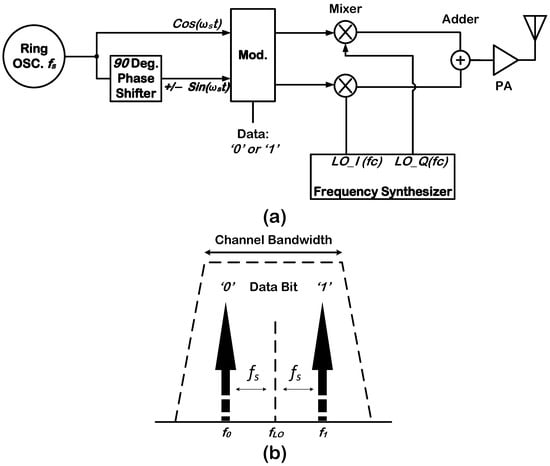
Figure 1.
(a) Traditional FSK transmitter block diagram. (b) Frequency plan for a simple 2LFSK modulation scheme.
To successfully obfuscate the FSK-modulated data during transmission, we propose a time-dependent frequency-variation method in which the FSK tones are generated by shifting the fLO within the bandwidth of the channel by ±∆f, thereby creating fLO ± ∆f tones. The precise value of the frequency shift, ∆f, is determined using the output of an off-chip TRNG. This way, an eavesdropping receiver will receive frequency-shifted FSK tones whose frequency shift, ∆f, is not known and is continuously changing based on the output of the TRNG, resulting in a poor signal-to-noise ratio (SNR) and a high bit error rate (BER) [14]. The frequency shift, ∆f, will be shared with the targeted receiver separately through a second asymmetrically encrypted channel, as needed. By doing so, the targeted receiver will correct the fLO with fLO ± ∆f, resulting in proper demodulation and acceptable BER in the targeted receiver [14]. In practice, the intended receiver does not require ∆f to be transmitted continuously. During the channel synchronization/setup, the transmitter securely shares the TRNG output state as a short seed (key) using a conventional asymmetric-key-based authenticated key exchange. The transmitter and receiver then generate an identical ∆f locally from this key, enabling correct de-obfuscation and demodulation, while an eavesdropper without the key observes an apparently random frequency offset [14]. The FSK transmitter output tones with/without proposed encryption are shown in Figure 2. Only two tones are displayed in the figure to avoid any confusion.
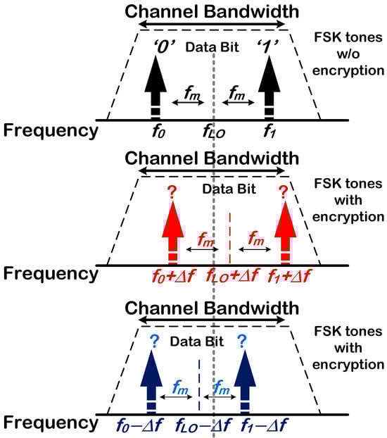
Figure 2.
FSK transmitter output tones with/without the proposed encryption.
3. Secure FSK Transmitter Front-End Design
The block diagram of the proposed secure FSK transmitter front-end is shown in Figure 3. The proposed design includes control units, a phase-locked loop (PLL) with a controllable VCO, mixers, and a power amplifier (PA). After the PLL calibrates the free-running frequency of the VCO by connecting the modulation switch, the control units tune the frequency of the VCO to modulate the signal, and I and Q signals are fed to mixers to drive the PA.
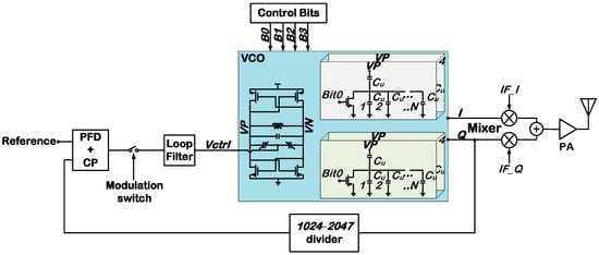
Figure 3.
Block diagram of the proposed secure FSK transmitter front-end.
Generation of Frequency-Shifted Tones
There are two methods to generate the frequency-shifted LO signals using a CMOS LC VCO. The first method is to add switch-controlled capacitors to the resonator capacitance, as shown in Figure 4a. By doing so, the frequency shifting can be expressed as follows:
where ΔC is the switch-controlled capacitance, L is the inductance of the resonator, C is the capacitance of the resonator, f0 is the LC VCO frequency when the switch is turned off, ΔC is excluded from the circuit, and Δf is the frequency shift once the switch is turned on and ΔC is connected to the circuit.
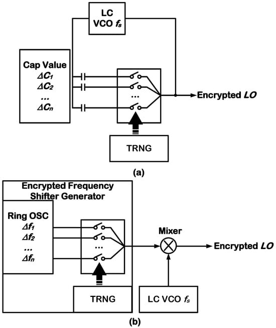
Figure 4.
(a) Direct tuning for generating a frequency-shifted LO signal, (b) using a mixer to generate the frequency-shifted LO.
The circuit topology using this method is simple to design and implement; however, it requires a very small ΔC value (≪1 fF) to get a fine frequency-shifting resolution. As an example, to realize a 10 kHz frequency shift, ΔC = 0.001 fF is needed for L = 4 nH, and f0 = 2.4 GHz. Such a small capacitance cannot be reliably created using any available on-chip capacitors in known integrated circuit (IC) fabrication technology.
The second method to generate a frequency-shifted LO signal is to mix the LO signal with a baseband signal generated by a low-frequency ring oscillator (Figure 4b). The main issue with using this method is the complexity of the architecture, which requires additional up-converters and LOs. Moreover, the design suffers from PVT (process, supply voltage, temperature) variation since the baseband ring oscillator frequency is not correlated to the LC VCO used in the LO, leading to inaccuracy during the frequency-shifting process. Therefore, the former solution is used for LO frequency shifting. However, the former solution still suffers from inaccuracies due to the use of a free-running LC VCO whose frequency is easily influenced by environmental parameters. To solve this problem, an innovative integer-N PLL-based calibration system is proposed to calibrate the VCO’s frequency when the modulation is in the rest mode (Figure 5). When the modulation is in the rest mode, the SW0 switch is closed. The switch SW0 is opened when the VCO is used to modulate the signal. The time needed to start the modulation varies with the settling time of the loop, but it could be as low as 10 µs [21]. As soon as the packet transmission is completed, the loop is closed for another 10 µs to recalibrate the VCO frequency. This process is repeated as needed. This way, the drift can be made smaller than 400 Hz during these intervals [21].
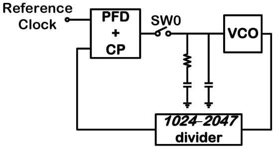
Figure 5.
Integer-N PLL-based calibration loop for the direct tuning method.
4. FSK Transmitter Front-End Implementation and Simulation Results
4.1. Design Implementation
Given the small BLE channel bandwidth (2 MHz) compared to the carrier frequency (~2.4 GHz), most conventional PLL designs employ fractional-N architectures to precisely control the VCO frequency, allowing for the use of high-frequency references to reduce the jitter. However, this is not necessary for the calibration loop, whose only job is to correct the VCO frequency and prevent deviation from the target channel. As such, this work uses a simple integer-N PLL architecture with a large divide ratio (>1024) to achieve 1 MHz frequency steps. The detailed schematics of the PLL blocks are shown in Figure 6. The proposed charge pump PLL uses a 2 MHz reference clock and consists of a phase–frequency detector (PFD), charge pump (CP), loop filter (LF), VCO, and divider. The divider employs a dual-modulus 2/3 prescaler to build a programmable frequency divider (Figure 6a). Each cell can divide the input clock (IN) by either two or three, controlled by the local control bit CON together with the handshake signals “modin” and “modout”. Inside the cell, two edge-triggered D flip-flops and a combinational logic form a synchronous counter; when configured for ÷2, the upper flip-flop simply toggles and the output frequency (OUT) is half of the input frequency; when “modin” is active, the logic forces one extra count using the lower flip-flop, realizing a ÷3 operation and generating “modout” to signal completion to the next stage. Cascading multiple 2/3 cells yields a wide-range programmable divider for the PLL.
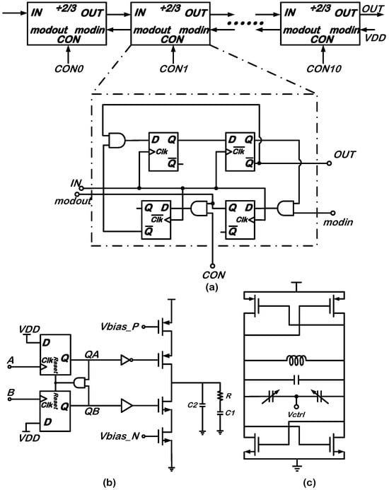
Figure 6.
Detailed schematics of the PLL: (a) 1024–2047 divider, (b) PFD and CP, and (c) VCO.
The PFD is benefiting from a conventional D-flip-flop-based phase–frequency detector topology with an asynchronous reset (Figure 6b). The D inputs are tied to VDD, so each flip-flop sets its Q output high on the first rising edge of its clock input (A or B), generating the UP (QA) and DOWN (QB) signals. When both outputs are high, the reset path clears both flip-flops, so the UP/DOWN pulse widths are proportional to the phase/frequency difference between A and B. The average PFD gain is 1/(2π) (rad−1).
The CP is also shown in Figure 6b; the charge pump uses PMOS and NMOS current sources biased by Vbias_N and Vbias_P, with switches driven by the PFD outputs A and B to selectively source or sink current at the output node. The loop filter is a second-order passive RC network with R = 86.5 kΩ, C1 = 58.3 PF, and C2 = 6.44 PF. The bandwidth of the loop is 94 kHz, and the phase margin is around 60°.
The complementary differential LC VCO (Figure 6c) with varactor tuning uses a cross-coupled NMOS/PMOS pair to provide the needed negative resistance and sustain the oscillation. The inductor, fixed capacitor, and voltage-controlled varactors set the oscillation frequency, which is tuned by the control voltage (VCTRL). The phase noise and the tuning curves of the VCO are shown in Figure 7a and Figure 7b, respectively.
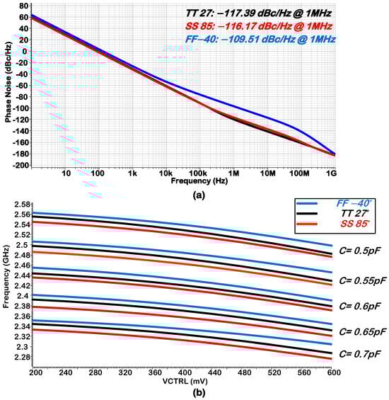
Figure 7.
LC VCO’s (a) phase noise and (b) tuning curves for different tuning varactor values (post-layout).
Figure 7a shows the post-layout simulated phase noise of the VCO under FF, TT, and SS process corners and extreme temperatures, with a maximum deviation of approximately 7.88 dB at a 1 MHz offset between the extreme cases. This limited variation indicates that process variations do not significantly impact the phase-noise performance, confirming the stability of the proposed architecture.
Figure 7b presents the post-layout simulation of the VCO tuning curves for the same corners, demonstrating that the oscillation frequency remains within the desired operating range in all cases, thus providing sufficient tuning margin and robustness against process variations.
The VCO occupies an active area of 230 µm × 272 µm. As shown in Figure 8a, the VCO core was laid out with strict differential symmetry to preserve matching and minimize systematic imbalance; the differential tank nodes and the cross-coupled pair were placed symmetrically, using common-centroid device placement and identical routing length and width to both tank nodes. Guard rings and isolation structures were implemented around the VCO core and its bias circuitry to mitigate substrate noise coupling. To control tank/inductor and interconnect parasitics, the inductor and critical tank routings were implemented in top metal using wide traces and very short connections to the LC tank, while high-swing nodes were physically separated from digital/control lines [22]. The switched capacitors were implemented using a replicated MOM unit-capacitor structure, with dummy elements surrounding the unit cells to mitigate edge effects (Figure 8b). All key performance metrics (frequency step resolution, tuning curve, and phase noise) were verified using post-layout extracted views with RC parasitic extraction included to confirm correct circuit operation.
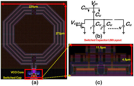
Figure 8.
(a) Layout of the VCO with switched capacitor. (b) The schematic of the switched capacitor with (c) a zoomed-in view of its layout.
4.2. Implementation of Sub-fF On-Chip Capacitance
Conventional capacitor banks employing series switches suffer from extra switch parasitics when turned off, complicating the realization of small capacitors. To solve this problem, a parallel scheme is employed [23]. As shown in Figure 8b, this scheme can ignore the parasites caused by the layout wire interconnection. By switching the VCTRL signal from low to high, the change in capacitance Cin when the switch changes from “off” to “on” state is denoted by ∆C:
where Cu is the unit capacitor in the given process node, and N is the number of the parallel unit capacitors at the bottom. N can be chosen to meet the minimum required capacitance variation. This scheme can ignore the parasitics and theoretically achieve sub-fF ∆C without any system error.
This work uses N = 5 to deliver ∆C ≈ 0.44 fF, which serves as the least significant bit (LSB) of the ∆C implemented by the capacitor bank. This ∆C is intended to achieve the minimum frequency shift (∆f) steps below 20 kHz. The Monte Carlo simulation is performed to determine the accuracy of the switched-capacitor LSB implementation. The resonance frequency of the parallel capacitor bank, when combined with the appropriate inductor, is simulated for LSB = 0 and LSB = 1 under a Monte Carlo process and mismatch variations (Figure 9). The simulated difference in the mean frequency for these two states is around 8 kHz, demonstrating the feasibility of the specified 10 kHz steps for the proposed LSB implementation. A 1000-run post-layout Monte Carlo simulation is performed to evaluate the resonance-frequency variation in the tank for the two capacitor-bank states. As shown in Figure 9a, for LSB = 0, the resonance-frequency distribution has a mean of 2.482139 GHz and a standard deviation of 2.29400 MHz. For LSB = 1, Figure 9b shows a mean of 2.482131 GHz and a standard deviation of 2.30668 MHz. The relatively large standard deviation reflects process and mismatch-induced variation in the absolute LC tank parameters; therefore, it mainly impacts the absolute resonance frequency. However, the effectiveness of the proposed LSB is best assessed by the separation between the two mean values, which is approximately 8 kHz. Importantly, process variation shifts the resonance frequency of both LSB states in the same direction (common-mode), while the relative frequency offset between LSB = 0 and LSB = 1 is preserved, confirming that the switched-capacitor LSB provides a consistent fine frequency step around the selected operating point.
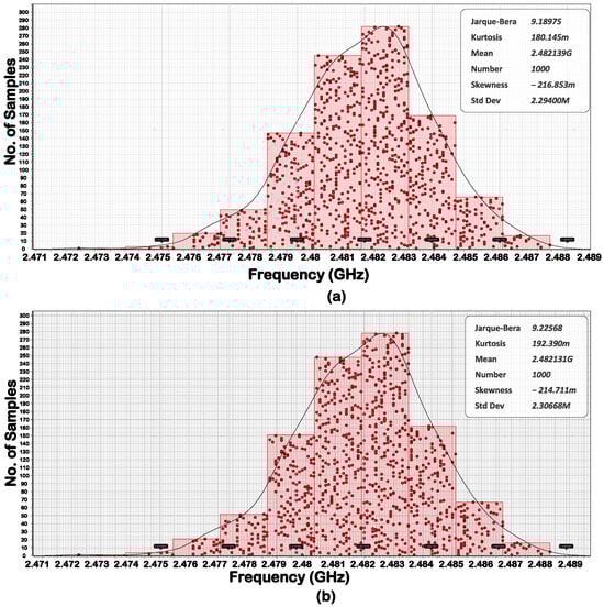
Figure 9.
Monte Carlo simulation results of the tank resonance frequency for (a) LSB = 0 and (b) LSB = 1.
4.3. Secure FSK Transmitter Front-End Simulation Results
To verify the functionality of the proposed secure FSK transmitter front-end, the system was implemented in a 22 nm FDSOI (Fully Depleted Silicon-On-Insulator) CMOS technology. As shown in Figure 10a, the PLL exhibits a setting time of ~25 µs, with a frequency variation of 2.46 kHz. During the FSK modulation and data transmission, the three-bit control signal achieves a minimum frequency-shifting step (LSB) ~ 16.39 kHz (Figure 10b). An external 55,500-bit TRNG output string was divided and applied to the three-bit control nodes with a period of 250 ns.
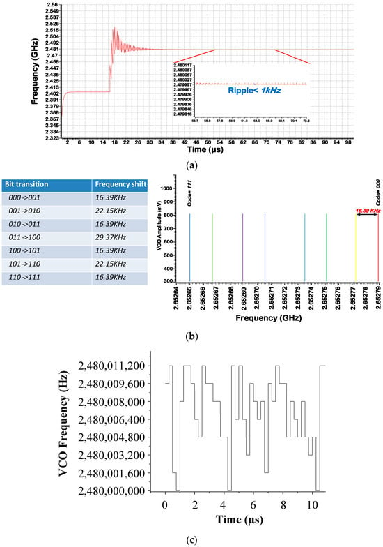
Figure 10.
(a) PLL transient simulation results, (b) encrypted LO tones corresponding to the three-bit control code, (c) transient simulation results of the TRNG output and the corresponding LO frequency.
To analyze the randomness of the data produced at the output of the transmitter, the Hamming distance of the 55,500-bit TRNG output was first computed as 13,646, when it was equally split into two 27,750-bit binary strings, representing a data duplication ratio of 49%. The Hamming distance of 20 sets of 2000-bit binary data truncated from the above 55,500-bit TRNG output was also statistically analyzed. The mean of the Hamming distance is 49.18%, and the standard deviation is 0.906%, indicating a good level of randomness in the data. In Figure 10c, the eight levels of the VCO output frequency are presented when the three-bit control signal with a period of 250 ns is applied, confirming the validity of the proposed frequency-shifting-based obfuscation for the FSK-modulated data.
5. Conclusions
A 2.4 GHz secure FSK transmitter front-end, which uses random frequency shifting to obfuscate the data, is presented. Implemented in a 22 nm FDSOI CMOS technology, the proposed secure transmitter uses an innovative capacitor-bank structure with a PLL-calibrated DCO to perform frequency shift in the LO frequency. Using a combination of parallel switch and series capacitors, the impact of the layout parasitics and switch parasitics on the LSB is minimized, allowing for reliable creation of sub-fF unit capacitance variation and, consequently, very small frequency-shifting steps (as low as 16 kHz). Using a 55,000-bit TRNG, the proposed transmitter front-end demonstrates the ability to generate 8-FSK signals with random frequency-shifting obfuscation.
Author Contributions
Conceptualization, Y.Q.; methodology, Y.Q. and H.M.L.; validation, Y.Q. and H.Y.; formal analysis, Y.Q., H.Y., and H.M.L.; investigation, Y.Q. and H.Y.; resources, H.M.L.; writing—original draft preparation, Y.Q., H.Y., and H.M.L.; writing—review and editing, H.Y. and H.M.L.; visualization, Y.Q.; supervision, H.M.L.; funding acquisition, H.M.L. All authors have read and agreed to the published version of the manuscript.
Funding
This work was funded by Semiconductor Research Corporation, grant number 2020-hw-2996.
Data Availability Statement
The original contributions presented in this study are included in the article. Further inquiries can be directed to the corresponding author.
Acknowledgments
The authors would like to thank students and staff at the Electro Science Laboratory at Ohio State University for providing the TRNG binary output data.
Conflicts of Interest
The authors declare no conflicts of interest. The funders had no role in the design of the study; in the collection, analyses, or interpretation of data; in the writing of the manuscript; or in the decision to publish the results.
Abbreviations
The following abbreviations are used in this manuscript:
| FSK | Frequency Shift Keying |
| TRNG | True Random Number Generator |
| DCO | Digitally Controlled Oscillator |
| BLE | Bluetooth Low Energy |
| IoT | Internet of Things |
| SNR | Signal-to-Noise Ratio |
| PLL | Phase-Locked Loop |
| LO | Local Oscillator |
| BER | Bit Error Rate |
| AES | Advanced Encryption Standard |
| ECC | Elliptic Curve Cryptography |
| ASIC | Application-Specific Integrated Circuit |
| RF | Radio Frequency |
| MSK | Minimum Shift Keying |
| 2LFSK | 2-Level Frequency Shift Keying |
| FDSOI | Fully Depleted Silicon-On-Insulator |
References
- Tamura, M.; Takano, H.; Nakahara, H.; Fujita, H.; Arisaka, N.; Shinke, S. A 0.5-V BLE transceiver with a 1.9-mW RX achieving −96.4-dBm sensitivity and −27-dBm tolerance for intermodulation from interferers at 6- and 12-MHz offsets. IEEE J. Solid-State Circuits 2020, 55, 3376–3386. [Google Scholar] [CrossRef]
- Liu, H.; Sun, Z.; Tang, D.; Huang, H.; Kaneko, T.; Deng, W. An ADPLL-centric bluetooth low-energy transceiver with 2.3mW interference-tolerant hybrid-loop receiver and 2.9mW single-point polar transmitter in 65 nm CMOS. In Proceedings of the IEEE International Solid-State Circuits Conference (ISSCC), San Francisco, CA, USA, 11–15 February 2018. [Google Scholar]
- Ding, M.; Wang, X.; Zhang, P.; He, Y.; Traferro, S.; Shibata, K. A 0.8V 0.8mm2 bluetooth 5/BLE digital-intensive transceiver with a 2.3mW phase-tracking RX utilizing a hybrid loop filter for interference resilience in 40nm CMOS. In Proceedings of the IEEE International Solid-State Circuits Conference (ISSCC), San Francisco, CA, USA, 11–15 February 2018. [Google Scholar]
- Kuo, F.-W.; Ferreira, S.B.; Chen, H.-N.R.; Cho, L.-C.; Jou, C.-P.; Hsueh, F.-L.; Madadi, I.; Tohidian, M.; Shahmohammadi, M.; Babaie, M.; et al. A Bluetooth low-energy transceiver with 3.7-mW all-digital transmitter, 2.75-mW high-IF discrete-time receiver, and TX/RX switchable on-chip matching network. IEEE J. Solid-State Circuits 2017, 52, 1144–1162. [Google Scholar] [CrossRef]
- Wong, A.C.W.; Dawkins, M.; Devita, G.; Kasparidis, N.; Katsiamis, A.; King, O.; Lauria, F.; Schiff, J.; Burdett, A.J. A 1V 5mA multimode IEEE 802.15.6/Bluetooth low-energy WBAN transceiver for biotelemetry applications. In Proceedings of the IEEE International Solid-State Circuits Conference (ISSCC), San Francisco, CA, USA, 19–23 February 2012. [Google Scholar]
- Liu, Y.-H.; Huang, X.; Vidojkovic, M.; Ba, A.; Harpe, P.; Dolmans, G.; de Groot, H. A 1.9 nJ/b 2.4 GHz multistandard (Bluetooth low energy/Zigbee/IEEE 802.15.6) transceiver for personal/body-area networks. In Proceedings of the IEEE International Solid-State Circuits Conference Digest of Technical Papers (ISSCC), San Francisco, CA, USA, 17–21 February 2013. [Google Scholar]
- Devita, G.; Wong, A.C.W.; Dawkins, M.; Glaros, K.; Kiani, U.; Lauria, F.; Madaka, V.; Omeni, O.; Schiff, J.; Vasudevan, A.; et al. A 5 mW multi-standard Bluetooth LE/IEEE 802.15.6 SoC for WBAN applications. In Proceedings of the 40th European Solid State Circuits Conference (ESSCIRC), Venice Lido, Italy, 22–26 September 2014. [Google Scholar]
- Sano, T.; Mizokami, M.; Matsui, H.; Ueda, K.; Shibata, K.; Toyota, K.; Saitou, T.; Sato, H.; Yahagi, K.; Hayashi, Y. A 6.3 mW BLE transceiver embedded RX image-rejection filter and TX harmonic-suppression filter reusing on-chip matching network. In Proceedings of the IEEE International Solid-State Circuits Conference (ISSCC) Digest of Technical Papers, San Francisco, CA, USA, 22–26 February 2015. [Google Scholar]
- Liu, Y.-H.; Bachmann, C.; Wang, X.; Zhang, Y.; Ba, A.; Busze, B.; Ding, M.; Harpe, P.; van Schaik, G.-J.; Selimis, G.; et al. A 3.7 mW-RX 4.4 mW-TX fully integrated Bluetooth Low-Energy/IEEE 802.15.4/proprietary SoC with an ADPLL-based fast frequency offset compensation in 40 nm CMOS. In Proceedings of the IEEE International Solid-State Circuits Conference (ISSCC) Digest of Technical Papers, San Francisco, CA, USA, 22–26 February 2015. [Google Scholar]
- Bachmann, C.; Vidojkovic, M.; Huang, X.; Lont, M.; Liu, Y.-H.; Ding, M.; Busze, B.; Gloudemans, J.; Giesen, H.; Sbai, A.; et al. A 3.5 mW 315/400 MHz IEEE 802.15.6/proprietary mode digitally-tunable radio SoC with integrated digital baseband and MAC processor in 40 nm CMOS. In Proceedings of the Symposium on VLSI Circuits (VLSI Circuits), Kyoto, Japan, 17–19 June 2015. [Google Scholar]
- Prummel, J.; Papamichail, M.; Willms, J.; Todi, R.; Aartsen, W.; Kruiskamp, W.; Haanstra, J.; Opbroek, E.; Rievers, S.; Seesink, P.; et al. A 10 mW Bluetooth low-energy transceiver with on-chip matching. IEEE J. Solid-State Circuits 2015, 50, 3077–3088. [Google Scholar] [CrossRef]
- Kuo, F.-W.; Ferreira, S.; Babaie, M.; Chen, R.; Cho, L.-C.; Jou, C.-P.; Hsueh, F.-L.; Huang, G.; Madadi, I.; Tohidian, M.; et al. A Bluetooth low-energy (BLE) transceiver with TX/RX switchable on-chip matching network, 2.75 mW high-IF discrete-time receiver, and 3.6 mW all-digital transmitter. In Proceedings of the IEEE Symposium on VLSI Circuits (VLSI-Circuits), Honolulu, HI, USA, 15–17 June 2016. [Google Scholar]
- Cagua, G.; Gauthier-Umaña, V.; Lozano-Garzon, C. Implementation and performance of lightweight authentication encryption ASCON on IoT devices. IEEE Access 2025, 13, 16671–16682. [Google Scholar] [CrossRef]
- Ellicott, S.; Kines, M.; Khalil, W.; Qi, Y.; Kurtoglu, A.; Miri Lavasani, H. Analog-inspired hardware security: A low-energy solution for IoT trusted communications. In Proceedings of the IEEE International System-on-Chip Conference (SOCC), Las Vegas, NV, USA, 14–17 September 2021. [Google Scholar]
- Bhanot, R.; Hans, R. A review and comparative analysis of various encryption algorithms. Int. J. Secur. Appl. 2015, 9, 289–306. [Google Scholar] [CrossRef]
- ALRikabi, H.T.S.; Hazim, H.T. Enhanced data security of communication system using combined encryption and steganography. Int. J. Interact. Mob. Technol. 2021, 15, 144–157. [Google Scholar] [CrossRef]
- Valenti, M.C.; Torrieri, D.; Ferrett, T. Noncoherent physical-layer network coding with FSK modulation: Relay receiver design issues. IEEE Trans. Commun. 2011, 59, 2595–2604. [Google Scholar] [CrossRef]
- Abidi, A.A. Direct-conversion radio transceivers for digital communications. IEEE J. Solid-State Circuits 1995, 30, 1399–1410. [Google Scholar] [CrossRef]
- Oh, S.; Kim, S.; Ali, I.; Nga, T.T.K.; Lee, D.; Pu, Y.; Yoo, S.-S.; Lee, M.; Hwang, K.C.; Yang, Y.; et al. A 3.9 mW Bluetooth low-energy transmitter using all-digital PLL-based direct FSK modulation in 55 nm CMOS. IEEE Trans. Circuits Syst. I Regul. Pap. 2018, 65, 3037–3048. [Google Scholar] [CrossRef]
- McClaning, K. Wireless Receiver Design for Digital Communications; IET: Stevenage, UK, 2012. [Google Scholar]
- Masuch, J.; Delgado-Restituto, M. A Sub-10 nJ/b +1.9-dBm Output Power FSK Transmitter for Body Area Network Applications. IEEE Trans. Microw. Theory Tech. 2012, 60, 1413–1423. [Google Scholar] [CrossRef]
- Lee, M.; Park, C. A 2.4-GHz VCO using a symmetric layout technique to minimize mismatches in differential signals. In Proceedings of the International Conference on Information Networking (ICOIN), Chiang Mai, Thailand, 10–12 January 2018. [Google Scholar]
- Pletcher, N.M.; Rabaey, J.M. A 100/spl mu/W, 1.9 GHz oscillator with fully digital frequency tuning. In Proceedings of the European Solid-State Circuits Conference, Grenoble, France, 12–16 September 2005. [Google Scholar]


Disclaimer/Publisher’s Note: The statements, opinions and data contained in all publications are solely those of the individual author(s) and contributor(s) and not of MDPI and/or the editor(s). MDPI and/or the editor(s) disclaim responsibility for any injury to people or property resulting from any ideas, methods, instructions or products referred to in the content. |
© 2026 by the authors. Licensee MDPI, Basel, Switzerland. This article is an open access article distributed under the terms and conditions of the Creative Commons Attribution (CC BY) license.