1. Introduction
Microdisplays are a key component in near-to-eye (NTE) devices, and they are widely used for augmented reality (AR) and virtual reality (VR) applications [
1,
2]. Most of these devices operate with batteries, and reducing the energy consumption of the microdisplay would increase the battery lifetime substantially. Microdisplays using organic light-emitting diode-on-silicon (OLEDoS) have the benefits of the standard complementary metal oxide semiconductors (CMOS) process and organic light-emitting diodes (OLEDs) combined. This technology is popular for AR and VR applications because of its high contrast ratio, high color reproducibility, fast optical response, and low power consumption [
3,
4,
5,
6,
7].
Reducing the power consumption of microdisplays is critical for portable electronic devices, as it is one of the most power-intensive components [
8]. Among the various peripheral circuits of a display, the data driver consumes the most energy. As display technology advances, resolutions, pixel densities (PPIs), and refresh rates increase, necessitating larger capacitors and higher data frequencies, which results in more dynamic power consumption by the drivers.
Numerous research efforts have been dedicated to mitigating the power consumption of OLED displays without compromising other critical display characteristics [
9,
10,
11,
12,
13]. One approach involves the utilization of power management techniques, such as adaptive voltage scaling, to dynamically adjust the power supply in response to the display content [
9,
10]. Another approach entails the implementation of adaptive refresh rates or the employment of SRAM-based pixel circuits to reduce the required refresh rate for low-data rate scenarios [
11]. Furthermore, investigations have been carried out to leverage low-leakage transistors or enhance overall AMOLED display efficiency through material engineering [
12]. However, most of the existing circuit methods are tailored for specific applications characterized by dark backgrounds or low data rates. As a result, there is a pressing need for a novel approach that can effectively reduce driver power consumption even in scenarios involving bright images or high data rates.
Another effective approach to reducing the dynamic power consumption of drivers is the charge recycling technique [
14,
15,
16,
17]. This method involves recycling dynamic energy to be used in the subsequent frame for partially charging the data lines. Previous research has predominantly focused on TFT-LCD displays that use dot inversion and analog data-driving techniques [
14,
15,
16]. Dot inversion has an inherent characteristic that allows for predicting whether the data lines will charge or discharge, making it relatively straightforward to manage the dynamic power consumption between data lines. Consequently, these studies have leveraged this predictability to employ shared control signals for the data lines [
14]. Applying this technique to digitally driven AMOLED displays is significantly more challenging because the charging or discharging of data lines is entirely dependent on the image content and cannot be predicted in advance. For digitally driven AMOLED displays, it is essential to control charge-sharing switches individually, considering their previous and next state conditions. This paper proposes a solution for utilizing this technique in AMOLED displays.
This paper introduces a data driver that incorporates an energy recycling technique for digitally driven OLEDoS microdisplays. This technique utilizes the energy stored on a data line before discharging it to the ground, allowing for partial charging of other data lines or a capacitor bank. This results in a reduction in the amount of energy required from the power supply, leading to a significant reduction in the dynamic power consumption of the data driver. The paper provides an overview of the conventional display architecture and baseline data driving method in
Section 2 and proposes a display architecture that incorporates the energy recycling technique for the data driver in
Section 3. The experimental results of
Section 4 present a block-level energy consumption breakdown of the microdisplay array and demonstrate the advantages of the proposed technique in reducing dynamic power consumption. The paper concludes in
Section 5.
2. Baseline Display
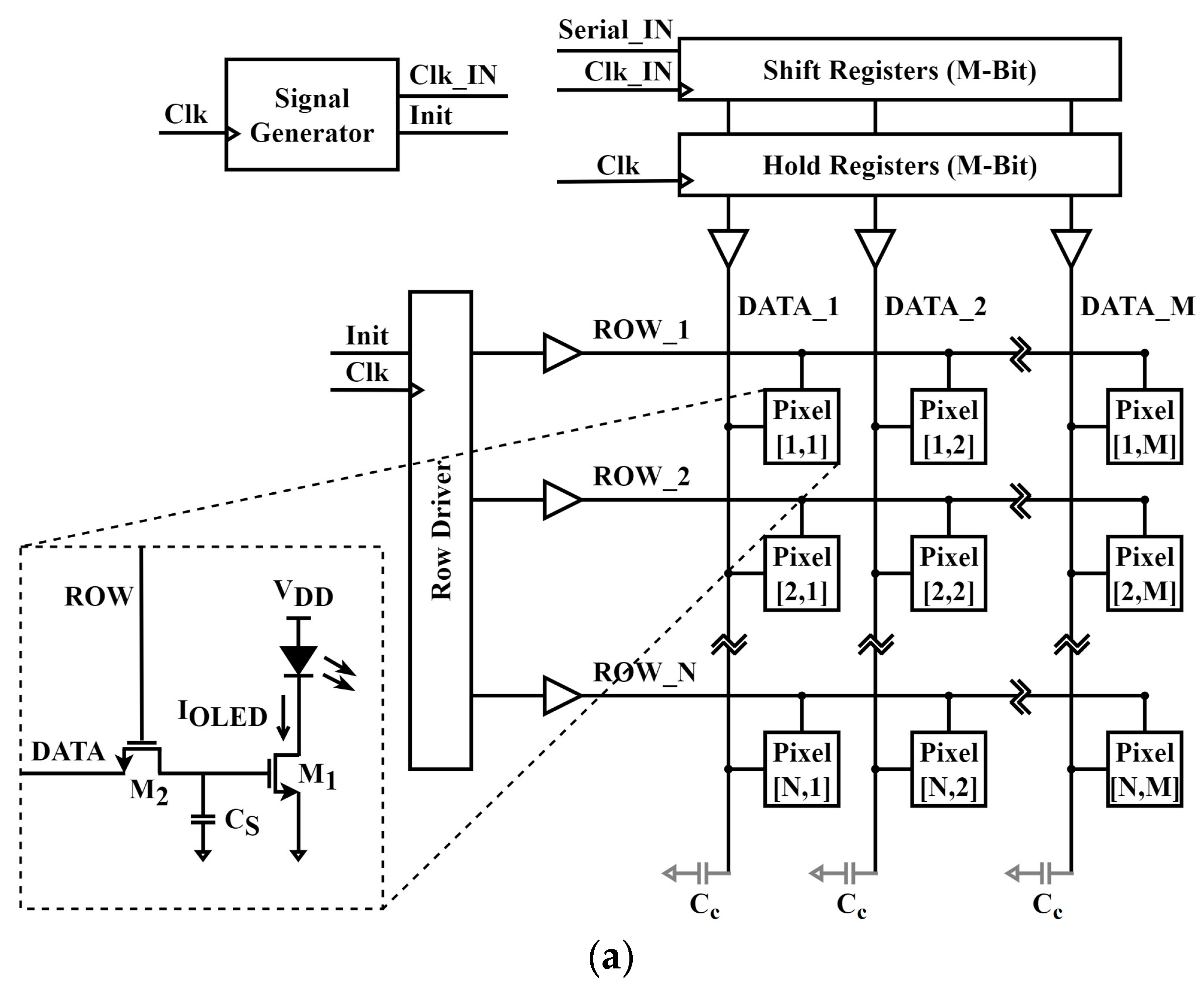
Figure 1a shows the peripheral circuitry (i.e., data and row driver and the signal generator) and the pixel array of an N × M AMOLED display. Without a loss of generality, the conventional 2T1C pixel circuit is chosen as the baseline pixel circuit. Here, we present the overall capacitance of a data line with a capacitor named C
C at the end of each data line. This capacitor is used to represent the total parasitic capacitance of the interconnects as well as the source/drain capacitance of pixel circuits in a data line.
Microdisplays are typically driven using either analog or digital data driving (also referred to as pulse width modulation (PWM)) methods. Unlike the analog data driving technique, where driving transistors function in the saturation region, the digital driving method simplifies the process by merely switching the pixel on or off, with the driving transistor operating in the linear region. Additionally, digital displays present advantages in terms of integration into fully digital systems [
18]. In a PWM-driven display with
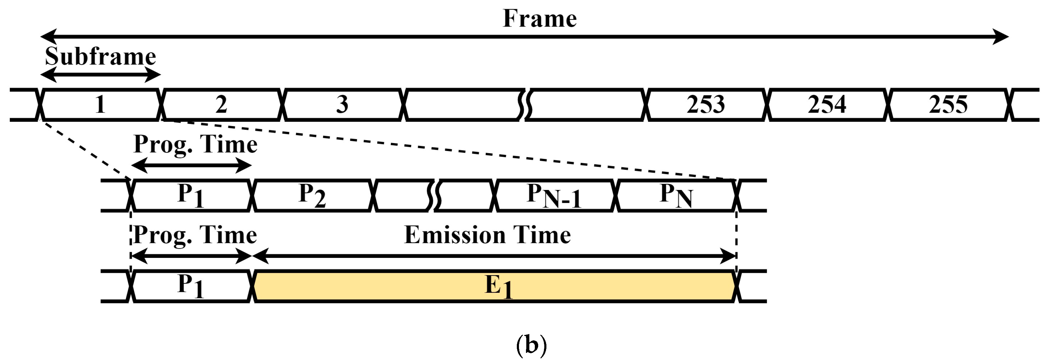
n bits, each frame is divided into (2
n) − 1 subframes of equal size.
Figure 1b illustrates this concept for an 8-bit display where each subframe is composed of a programming and emission time pair. It is important to note that the emission time must be long enough for the row driver to program all other rows. The PWM data driving method, as described earlier, is employed in this paper.
3. Data Driver Energy Recycling Technique
The data driver is the most power-intensive component in the display’s peripheral circuitry. Considering this and the increase in dynamic power consumption resulting from advancements in display characteristics, it is critical to reduce the dynamic power consumption of the data driver to enhance overall energy efficiency.
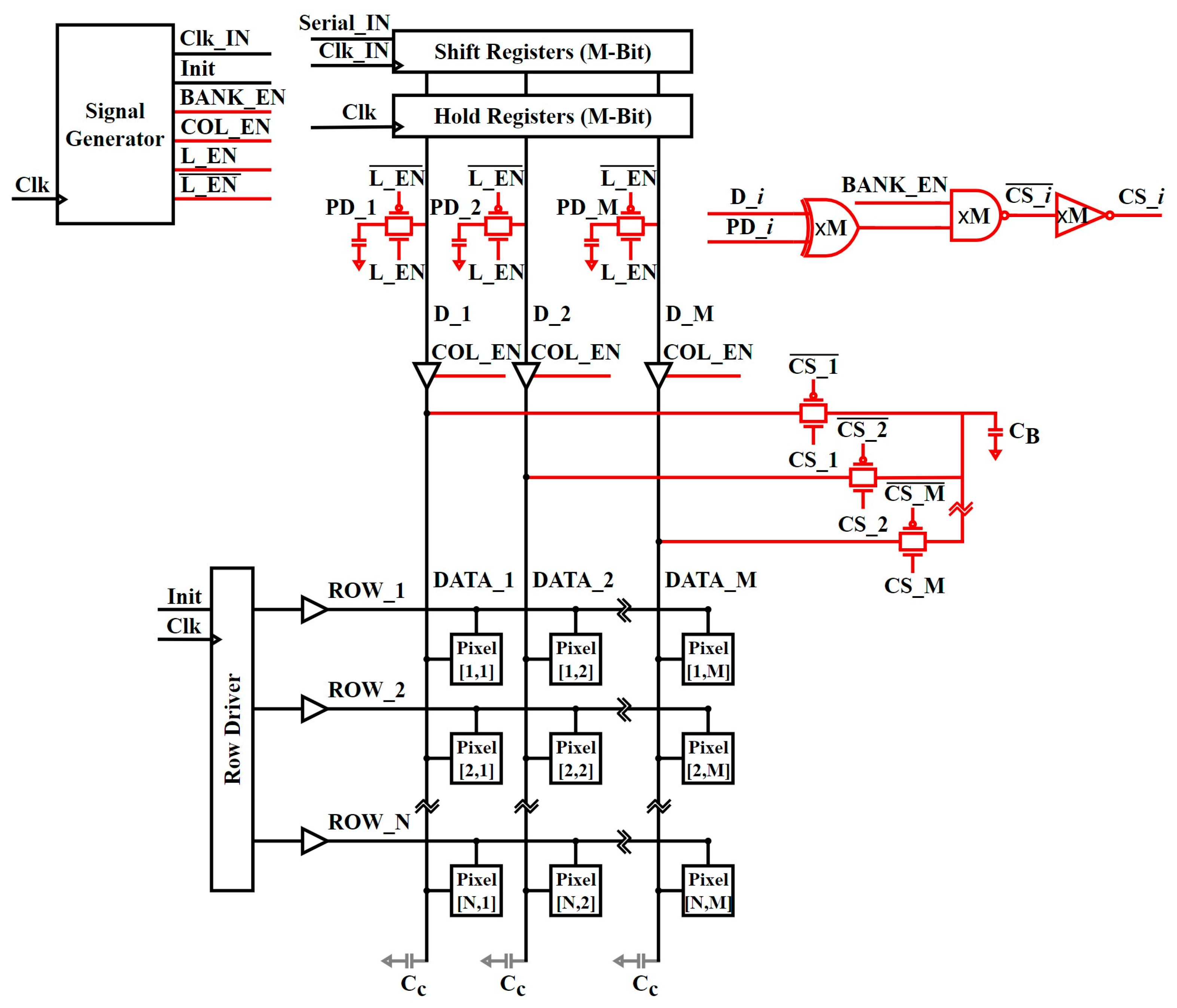
Figure 2 shows implementation of the energy recycling technique on the data driver. To implement the energy recycling feature, the following circuit components have been added to each data line: (1) a data storage unit (i.e., storage capacitor) to store the previous value of the data; (2) a transmission gate utilized as a switch to connect the capacitor of the data line (C
C) to the capacitor bank (C
B); (3) a circuit to generate the charge recycling signal (i.e., CS_
i) for enabling and disabling the transmission gates. In addition, a shared capacitor bank (C
B) and control signals generated in the signal generator block are also required.
At each charge recycling interval, a data line will be connected to the bank in two scenarios: (1) If the current data value on the data line is ‘1’ and the next data value is ‘0’. This means that the energy on the CC capacitor of the line is going to be discharged to the ground. Therefore, first, a portion of energy will be stored in the capacitor bank (CB) and, later, the remaining energy will be discharged to the ground. These data lines are referred to as donor data lines during this specific recycling interval. (2) If the current data value on the data line is ‘0’ and the next data value is ‘1’, the data line is referred to as an acceptor data line, as it receives some energy from the capacitor bank and is then fully charged to VDD using the supply voltage. In cases where the data value remains unchanged between two consecutive programming cycles, the data line is not connected to the capacitor bank and retains its value.
As previously stated, each data line incorporates a circuit that generates its corresponding charge recycling signal (CS_j), which is responsible for enabling or disabling the connection to the capacitor bank. This circuit utilizes an XOR gate to identify any variation between the previous data (PD_j) and current data (D_j) values. During the recycling interval (activated by the BANK_EN signal), if a discrepancy exists between the current and previous data values, the NAND and inverter gates produce an output that links the data line to the capacitor bank via the data line transmission gate for the duration of the recycling interval.
Figure 3 illustrates the timing diagram of the control, row, and data signals for six consecutive programming times of the
jth data line, assuming a data sequence of “0100110”. The signal L_EN is enabled in each programming time and stores the data on a small capacitor that later, in the next programming time, are used as the previous data (PD_
j).
At the beginning of the first programming time, the data line’s buffer is disconnected from the supply voltages (COL_EN = ’0’). At the time t1, the current data value (D_j) is ‘1’ and the previous data value (PD_j) is ‘0’; therefore, the data line’s XOR gate output is ‘1’. Since the bank enable signal (BANK_EN) is enabled at time t1 and the output of the XOR is ‘1’, at that time the data line’s charge recycling signal (CS_j) will be enabled. So, the transmission switch of this data line turns on to connect it to the capacitor bank to receive energy from the bank.
Note that, during this charge recycling interval, all data lines whose previous and current data values are different will be connected to the capacitor bank at the same time. Those data lines that currently have a value of ‘1’ will be the donor of the energy and those that currently have a value of ‘0’ will be the acceptor of the energy from the bank and other data lines. At the time t2, this new data value will be stored in the storage unit’s capacitor for comparison in the next programming cycle. Also, since the COL_EN is enabled, the capacitor of the data line will be fully charged to VDD via the PMOS transistors in the data line’s buffer. At time t3, the previous data value is ‘1’ and the next data value is ‘0’, so the data line will be connected to the bank to donate a portion of its energy. It will be fully discharged at time t4 when the data line’s buffer is enabled. At the charge recycling interval of the third row’s programming time, the previous and next data values are both ‘0’, and the data line is not connected to the bank. Later, for programming the fourth row, the data line receives some energy from the bank. It will hold the value of ‘1’ at the charge recycling interval of the fifth row because the previous data value and the next data value are both ‘1’. Finally, at the charge recycling interval of the sixth row, because the next value is ‘0’ the data line donates a part of the energy to the bank and then fully discharges.
It should be noted that the proposed method can also be implemented without the capacitor bank, which can help to save on area. In such a scenario, there is no energy reservoir to transfer energy between programming cycles. Instead, during each programming cycle, the available donor data lines will transfer some of their energy to the existing acceptor data lines. The capacitor bank plays a crucial role in transferring energy between programming cycles and serves as an energy reservoir. It is especially beneficial in cases where there are insufficient donor data lines during a specific programming cycle. For instance, in the case of an image with horizontal black-and-white strips, all data lines act as donors during the programming time of a black line and as acceptors during the programming time of a white line. Without the capacitor bank, there would be no energy available to provide to the data lines when required. This is typically not the case for most real-life images, as there are usually both donor and acceptor data lines in each programming cycle. Therefore, the required size of the capacitor bank can be determined based on the characteristics of the images for the intended application of the display.
4. Experimental Results
To illustrate the extent of energy saving achieved by the proposed data driver, an experimental proof-of-concept 48 × 64 pixel array with its controller module, row driver, and data driver is designed and implemented using TSMC 65 nm technology. The controller module generates the signals for a VGA-sized (i.e., 480 × 640) display with a refresh rate of 60 Hz. The row and column capacitor per pixel has been extracted from the layout, and extra capacitors have been added at the end of each row and column to mimic the capacitive load of a VGA-sized array. The fabricated array has two modes, namely the conventional mode and the low-power mode. The micrograph of the test chip and the arrays’ layout implementation and size are shown in
Figure 4. A capacitor bank with a size of approximately 0.2 C
C or 100 fF per data line is used as the energy reservoir in our implementation. The capacitor bank’s area overhead accounts for 2.5% of the display’s total area and could have been avoided by using Metal–Insulator–Metal (MIM) capacitors on the data driver’s circuit instead of the MOSCAP that was employed.
The measurement setup of our implemented test chip is illustrated in
Figure 5a, and the packaged test chip depicted in
Figure 5b serves as the Device Under Test (DUT) in this setup. The FPGA board is programmed with a Verilog code, which generates various test images transmitted as a Serial IN signal to the DUT. Additionally, the code allows us to select different internal signals to be displayed on the oscilloscope for verification purposes. Within the setup, the data driver, signal generator, row driver, pixel array, and IO pads are separate voltage islands. Each of these voltage islands is supplied with the corresponding voltages by dedicated power supplies, except for the data driver whose power consumption we intend to measure. To measure the data driver’s power consumption, we connect its power supply to a KEITHLEY-2400 source meter. This instrument not only provides the supply voltage but also precisely measures the current drawn from that supply voltage. In this paper, power consumption is calculated by measuring the energy drawn from the supply voltage over a fixed frame duration. Given that the chosen refresh rate for the display is 60 Hz, the frame time is set at 16.6 ms. The power consumption of the data driver within a frame is determined by multiplying the average current during that frame by the supply voltage. Since the frame time remains constant, it simplifies the calculation of the energy consumption. Consequently, in this paper, the absolute values of power and energy exhibit a linear correlation.
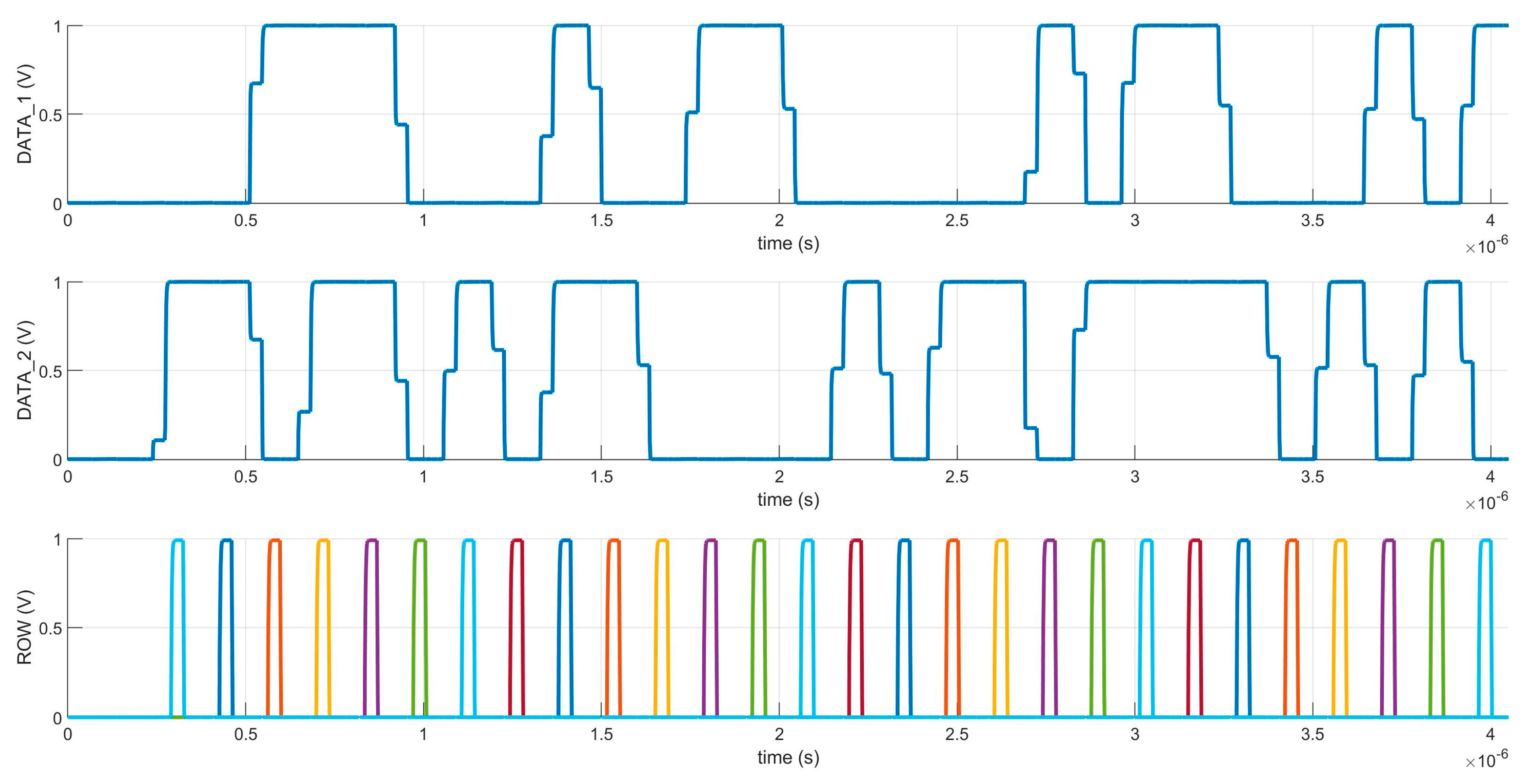
Figure 6 presents the data value waveforms of the first two data lines, depicting the programming of distinct pixel circuits on these lines. It also illustrates the row enable signals of the display during the initial 4 us of the frame time. The data value waveforms correspond to a randomly generated test image in which 50% of the pixels are black. It is evident from the figure that the level of restored voltage varies based on the number of available donor and acceptor data lines at each programming cycle as well as the amount of energy that is available in the capacitor bank.
Figure 7 depicts a set of 10 randomly generated test images, each characterized by varying black-to-white pixel ratios. These images were employed to evaluate the power consumption of the array.
Table 1 provides a comparative analysis of the measured power consumption of the array in both conventional and low-power modes. The design of the array allows for individual measurement of the power consumption of each primary block of the display driver. According to the measurement results, it was observed that the power consumption of the row driver and signal generator blocks remained unaffected by the image displayed, which was also consistent between both conventional and low-power data driver modes. The energy recycling overhead entry in the table includes the power consumption of the signal generator block, necessary for generating the required signals in the proposed method. The results indicate that the data driver’s power consumption can be 1.7–9.8 times higher than the row driver, depending on image content, highlighting its role as the most power-intensive component in the display’s peripheral circuits. The data driver’s power consumption is notably influenced by the test image, as observed in the conventional array. Specifically, the highest power consumption of the data driver occurs during the 50% random test image, which aligns with the expectation that the dynamic power consumption of the data driver is directly proportional to the level of data activity.
The low-power technique proposed in this study demonstrates the highest energy recycling when the number of donor and acceptor data lines is closely matched (e.g., 50% test image). The extent of energy recycling is directly proportional to the balance between the donor and acceptor data lines, and this effectiveness decreases as the balance between these lines becomes less optimal. In situations where there is an uneven number of donor and acceptor data lines between programming cycles, the presence of a capacitor bank generally aids in enhancing the overall power recycling capacity. The results obtained from measuring the array in the low-power mode demonstrate that, after accounting for the additional power consumption associated with the energy recycling circuitry, the data driver power is reduced by up to 20%. Furthermore, the overall power consumption of the driver, which includes the row driver, data driver, and signal generator, is reduced up to 18% with the utilization of the proposed technique. This power reduction is achieved specifically during the peak power consumption of the display. This finding highlights the potential benefits of the proposed method, especially in scenarios where there is a high data toggle rate and power consumption is a significant concern. It should be noted that, in the cases of white or black images, no energy recycling occurs due to the absence of donor and acceptor data lines. In fact, the overhead of the extra energy recycling circuitry in these extreme cases can result in a deterioration of the driver’s power consumption. The measurement results indicate that the overall driver power consumption may degrade by 8.6% in such scenarios. However, it is important to highlight that these cases are infrequent, and a power gating mechanism could be implemented to disable the extra circuitry for such rare occurrences. Furthermore, the measurement results reveal that, even with low data activity (e.g., 10% or 90% test images), the proposed low-power technique still yields benefits.
The previous tests focused on measuring the power consumption of the drivers for a subframe with a black-and-white image. However, to evaluate gray levels, it is necessary to run the display for a full frame and measure the power consumption accordingly. For this purpose, real-life test images from
Figure 8 were selected to examine the power consumption in a broader context.
Table 2 presents the power consumption of each test image for a full frame duration. Among the four real-life images used, the power consumption reduction in the drivers ranged from 7.5% for the Lenna image to 14.1% for the Houses image. As discussed previously, the effectiveness of this technique is more prominent when the data activity rate is higher in an image. Therefore, the Houses image, which exhibits a higher data activity compared to the Lenna image, achieves a greater amount of power saving. Based on the presented findings, it can be inferred that the proposed method offers distinct advantages, particularly in high data rate applications.
The proposed method effectively supports displays with higher resolution and refresh rates by employing larger switches, data line buffers, and a capacitor bank. We conducted simulations for an FHD (i.e., 1080 × 1920) display. For an FHD display featuring 8-bit color depth and a 120 Hz refresh rate, using the PWM data driving method shown in
Figure 1b, the programming time is 4.5 times shorter than that of a VGA display with a 60 Hz refresh rate. In addition, the intrinsic capacitance of each data line has been multiplied by 2.25 times in our simulations, which corresponds to the ratio of 1080 to 480. According to the simulation results, the average power reduction percentage for the data driver in an FHD display with a refresh rate of 120 Hz is 20%. The total power consumption of the driver is also reduced by 17.8%. Note that these results were obtained using 10 randomly generated black-and-white test images. As expected, when the display’s resolution and refresh rate increase, the proportion of dynamic power to total power also increases. As a result, the efficiency of the suggested energy restoration technique becomes more pronounced. Therefore, applying the proposed technique to high-resolution displays with higher PPI and refresh rates can significantly reduce overall power consumption, as dynamic power consumption has a more impactful role in displays with higher resolutions, PPIs, and refresh rates.


