Abstract
Deep-brain stimulation (DBS) is a highly effective and safe medical treatment that improves the lives of patients with a wide range of neurological and psychiatric diseases. It has been established as a first-line tool in the treatment of these conditions for the past two decades. Closed-loop deep-brain stimulation (CLDBS) advances this tool further by automatically adjusting the stimulation parameters in real time based on the brain’s response. In this context, this paper presents a low-noise amplifier (LNA) and a neurostimulator circuit fabricated using the low-power/low-voltage 65 nm CMOS process from TSMC. The circuits are specifically designed for implantable applications. To achieve the best tradeoff between input-referred noise and power consumption, metaheuristic algorithms were employed to determine and optimize the dimensions of the LNA devices during the design phase. Measurement results showed that the LNA had a gain of 41.2 dB; a 3 dB bandwidth spanning over three decades, from 1.5 Hz to 11.5 kHz; a power consumption of 5.9 µW; and an input-referred noise of 3.45 µVRMS, from 200 Hz to 11.5 kHz. The neurostimulator circuit is a programmable Howland current pump. Measurements have shown its capability to generate currents with arbitrary shapes and ranging from −325 µA to +318 µA. Simulations indicated a quiescent power consumption of 0.13 µW, with zero neurostimulation current. Both the LNA and the neurostimulator circuits are supplied with a 1.2 V voltage and occupy a microdevice area of 145 µm × 311 µm and 88 µm × 89 µm, respectively, making them suitable for implantation in applications involving closed-loop deep-brain stimulation.
1. Introduction
Deep-brain stimulation (DBS) is a surgical procedure that involves the implantation of a medical device called a neurostimulator (often referred to as a brain pacemaker) that sends mild impulses to specific areas of the brain through implanted electrodes [1]. The electrical currents used in DBS are very low, typically in the range of microamperes, and they are applied to strategic points, primarily located deep within the brain tissue. This procedure involves inserting implantable tips, with electrode rings at the ends, into specific points in the thalamus, the subthalamic region, and the globus pallidus, among other structures. The electrodes are connected to the neurostimulator via extension cables containing metallic wires [2]. The neurostimulator is a device with dimensions no larger than that of a matchbox and includes an attached battery to provide power for its operation [3]. The first use of the DBS technique dates back to 1997, when the American FDA, for the treatment of Parkinson’s disease [4], granted authorization for its use. Since then, the DBS has become a first-line therapy option for relieving symptoms associated with neurological and movement disorders that are unresponsive to other therapies, namely, chronic pain, dystonia, Parkinson’s disease, Tourette’s syndrome, essential tremor, obsessive–compulsive disorder, and morbid obesity [4].
There are two paradigms for classifying DBS, namely, open-loop DBS (also known as conventional DBS) and closed-loop DBS (also known as adaptive DBS or CLDBS) [3,5,6]. In the case of open-loop DBS, a neurologist manually adjusts the stimulation parameters every 3–12 months after implantation. On the other hand, for CLDBS, the adjustment of stimulation parameters is performed automatically based on some measured biomarkers [3,6]. Biomarkers are acquired signals, and they can have different natures, namely, bioelectrical, biochemical, and psychological, among others [3,6]. Biomarkers are essential indicators in CLDBS because, based on the disease to be treated, they help to adaptively reconfigure the signals used in neurostimulation [3,6].
Advances in microelectronics are paving the way for the simultaneous acquisition of multiple types of biopotentials using a single device, enhancing CLDBS. The development of the CMOS blocks presented in this paper was motivated by this capability.
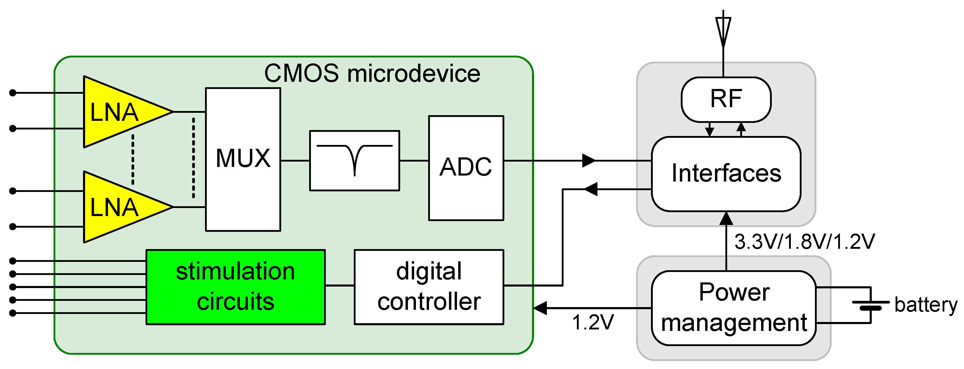
Figure 1 illustrates the block diagram of a system designed for applications in CLDBS. The diagram comprises three main modules: the power management module, the RF communications module, and the CMOS microdevice, which serves as the front-end circuit. The CMOS microdevice is responsible, on one hand, for acquiring neuronal signals, filtering them, and converting them to a digital format. Furthermore, it is responsible for applying neuronal stimuli according to received instructions. Of particular significance within the CMOS microdevice are two pivotal circuits: the low-noise amplifier (LNA) and the neurostimulator, depicted respectively in yellow and green colors in the block diagram.
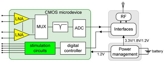
Figure 1.
Block diagram of a system for applications in CLBDS. The system is composed of a power management module, a communications module, and the CMOS microdevice, containing the acquisition blocks, the neurostimulator, and the control block. The proposed circuits, LNA, and the neurostimulator are filled with the yellow and green colors, respectively.
In this paper, we present an LNA and a neurostimulator circuit designed specifically for implantable applications. The LNA is based on a simple differential amplifier configuration, and its design and optimization were accomplished through the application of metaheuristic algorithms. The circuit can capture local field potentials (LPFs), characterized by frequencies below 200 Hz and amplitudes under 5 mV, but it is primarily optimized for action potentials (APs), with frequencies ranging from 200 Hz to 7 kHz and amplitudes under 200 μV [7]. The neurostimulator circuit was designed to generate arbitrary current pulses with a biphasic shape. Both circuits were implemented in a 65 nm CMOS process. The rest of this paper is organized as follows: Section 2 presents the circuit designs, Section 3 details the experimental results, Section 4 provides comparisons between our circuits and others found in the literature, and, finally, Section 5 concludes the paper.
2. Design
In this section, the LNA and the neurostimulator designs are presented.
2.1. Low-Noise Amplifier (LNA)
Signals at the input of an LNA present a variety of challenges, such as low amplitudes, on the order of microvolts, and low frequencies, close to 0 Hz. The amplifiers for neural recordings, found in the literature, typically exhibit a mid-band gain of 40 dB, with bandwidths ranging from sub-hertz to a few kilohertz or even a few dozen kilohertz [8,9,10,11,12,13].
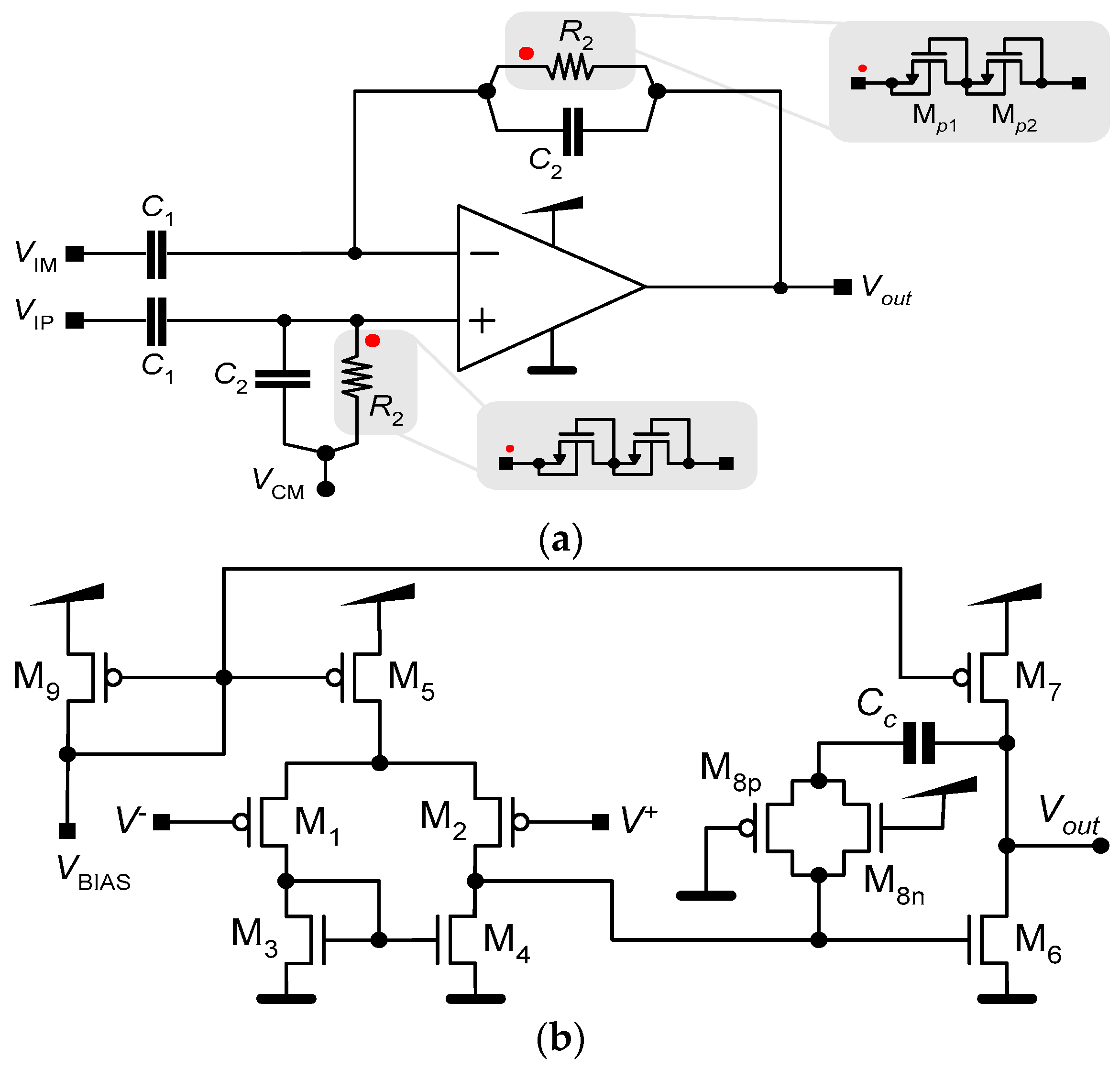
LNAs are usually implemented using a high-gain amplifier and capacitive feedback, where capacitors are employed to set the gain and achieve a DC offset rejection [7,14]. Figure 2a shows a schematic of this configuration. It comprises a differential amplifier, two pairs of capacitors, C1 and C2, and a pair of large pseudo-resistors R2. The function of the resistors, together with the capacitors, is to generate a low cutoff frequency.
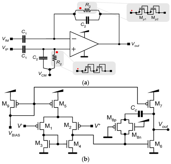
Figure 2.
Schematics of (a) an LNA and (b) the operational amplifier. The red dots on (a) indicate how the pseudo-resistors connects to the operational amplifier.
Instead of differential amplifiers, a single-input CMOS inverter can be used for amplification [7]. An LNA with a CMOS inverter has half the number of transistors in the amplifier compared to the input stage of a differential amplifier and, therefore, introduces approximately half the amount of power noise. However, they will exhibit high sensitivity to supply voltage variations and poor linearity [7,9].
A typical LNA implementation employs operational transconductance amplifiers (OTAs). Various OTA topologies, including both single and differential outputs, have been employed. A symmetrical OTA was utilized in [10], while a folded cascade was employed in [15]. Additionally, to suppress voltage offset and 1/f flicker noise, switched-capacitor techniques are often considered [7,14].
In our approach, we employ the simple OTA presented in Figure 2b. The OTA has a basic structure with two stages. The first stage is a differential pair that works as the input stage. The second stage is a common source amplifier and provides additional gain to the input stage, thereby increasing the total gain of the operational amplifier. The PMOS (M8p) and the NMOS (M8n) act as a resistor in series with the capacitor (Cc), creating a pole and ensuring that the operational amplifier is unconditionally stable. The transfer function of the LNA is given as follows:
where k = R2C1, Amband = (C1 + C2)/C2, fL = 1/(2πR2C2), and fH = fpA0/Amband = GBW/Amband. The quantities fp, GBW, and A0 are, respectively, the dominant pole, the gain × bandwidth product, and the open-loop gain of the operational amplifier. Typically, fL << fH and C2 << C1; then, for medium-frequency operation, i.e., for fL << frequency << fH, the LNA gain is as follows:
Af ≈ C1/C2 = Amband
Frequencies fL and fH are the LNA low and high cutoff frequencies, respectively.
Because capacitances in an integrated circuit are typically on the order of picofarads, the resistor (R2) must be on the order of teraohms to ensure that the low pole, fL = 1/(2πR2C2), of Af(s) has a value near or lower than 1.0 Hz. The integration of high-value resistors, like R2, in conventional form is not feasible because of the substantial area they would require. One feasible solution to this challenge involves implementing R2 through the utilization of pseudo-resistors [16], as depicted in Figure 2b.
To achieve low noise and low power, even using an OTA with a simple configuration, the LNA design in this work was carried out using metaheuristic algorithms, specifically particle swarm and simulated annealing [17,18]. To accomplish this task, a Matlab framework for transistor sizing and circuit optimization, based on metaheuristics, was applied [19,20]. For the calculation of the design score employed in the optimization, the attributes of the operational amplifier and of the complete LNA were taken into consideration. For the operational amplifier, the following attributes were considered: the differential gain (>80 dB), the common-mode rejection rate (CMRR) (>60 dB), the power supply rejection rate (PSRR) (>60 dB), the input common-mode range (from 0.5 V to 0.7 V), the slew rate (>0.08 V/μs), the systematic input voltage offset (<0.1 mV), and the phase margin (between 45° and 60° for an output capacitance of 0.7 pF); for the complete LNA, the considered attributes were as follows: the gain (between 39 dB and 41 dB), the input-referred noise (IRN) (<5.0 μVrms), the low and high cutoff frequencies (6.0 Hz and 7.0 kHz, respectively), the power consumption (minimum), and the area (minimum).
Thermal and biological noises in cortical recordings are approximately 10 μVrms [21,22], so the input-referenced noise of LNAs is expected to be lower than this value. A noise floor as low as 4.0 μVrms is typically pursued by neuronal amplifier designers, but this level is significantly below the levels of thermal and biological noises. Initially, during the design and optimization phase, an input noise of 4.0 μVrms was targeted. However, achieving this level of noise requires a significant amount of power consumption in the utilized process, because of various factors, such as the large gate capacitance of the differential pair transistors, M1 and M2. For this reason, in our design, we allowed for a higher input noise while maintaining low power consumption.
It should be noted that technologies with larger minimum dimensions but lower gate capacitances, such as 180 nm technologies, can be advantageously utilized in the design of low-noise LNAs.
Table 1 lists the dimensions of the MOSFETs of the operational amplifier and of the pseudo-resistors, and the values of the capacitors C1, C2, and Cc generated by the sizing/optimization algorithms. The simulated performance parameters of the LNA are a power consumption of 6.16 μW, for a power supply of 1.2 V; low and high cutoff frequencies of 12 Hz and 8.5 kHz, respectively; a gain of 39.9 dB; and input-referred noises (IRNs) of 3.93 μVRMS, from 12 Hz to 200 kHz, of 3.71 μVRMS, from 200 Hz to 8.5 kHz, and 5.4 μVRMS, from 12 Hz to 8.5 kHz. Additionally, the circuit is unconditionally stable for capacitive loads as high as 20 pF.

Table 1.
Dimensions of the MOSFETs that comprise the operational amplifier and the pseudo-resistors, and the values of the capacitors Cc, C1, and C2 obtained with the optimizer.
2.2. Neurostimulator
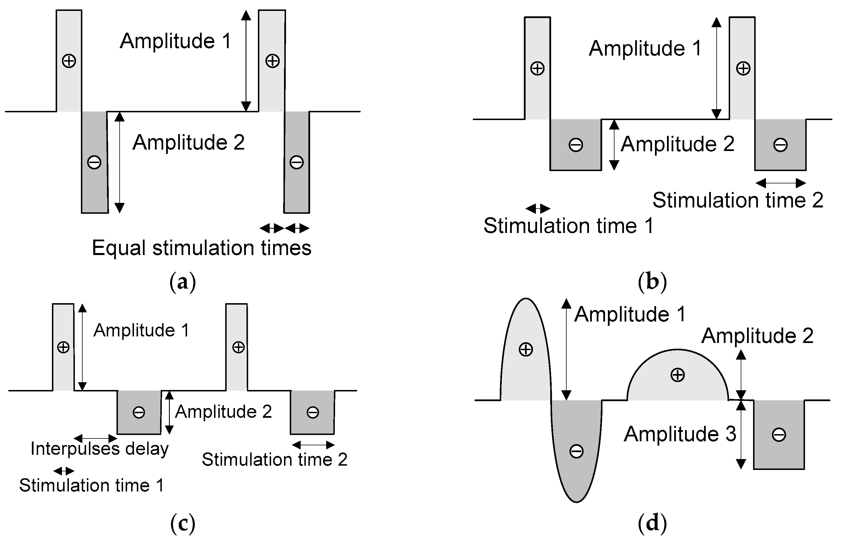
Neurostimulators must preferably provide current pulses with a biphasic shape because of electrical safety reasons, such as avoiding the accumulation of charges at interfaces between electrodes and ionic species within the neuronal tissue [23]. Figure 3 illustrates four examples of pulse shaping, where the duration (or stimulation times), frequency, amplitudes, and inter-pulse delay of the pulses can be set according to medical requirements. The mean value of these signals is zero in all the examples, thanks to the arbitrary pulse shaping.

Figure 3.
An example of (a) a symmetric biphasic pulse shape without an inter-pulse delay and a mean value of zero; two examples of asymmetric biphasic pulse shapes, with (b) zero and (c) non-zero inter-pulse delays; and an example of (d) a signal with an arbitrary shape. All the waves can have a mean value of zero.
To maintain electrical safety, as previously mentioned, the neurostimulator circuit was designed to offer the capability for generating current with a biphasic waveform, which can invert the direction of the charge injection in the neuronal tissue. The phenomenon of nullifying the charge accumulation is called the charge balance [23]. Traditionally, the inversion of the current direction requires a bridge with an H-topology [24], with the disadvantage of requiring four transistors for current inversion, increasing the programming complexity, and access to two different contact points on the electrodes, which are normally unipolar. For these reasons, the circuit responsible for injecting the current into the electrodes is based on the Howland current pump [25]. This circuit is easy to integrate because it uses low resistance values, that is, below 20 kΩ.
Figure 4a shows the schematic of the current pump that implements the neurostimulator. The neurostimulator is composed of an operational amplifier and four resistors {R1, R2, R3, R4}, all fully implemented using the mask layers of the TSMC 65 nm CMOS process. Figure 4b presents the schematic of the operational amplifier used by the current pump. Table 2 lists the dimensions of the MOSFETs, the values of the operational amplifier’s internal capacitances, Cc and Cx, and the values of the current-pump’s resistors.
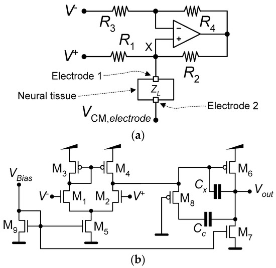
Figure 4.
Schematics of (a) the current pump that implements the neurostimulator and (b) the operational amplifier used by the current pump.

Table 2.
Dimensions of the MOSFETs, the capacitors (Cc and Cx) that comprise the operational amplifier, and the resistors of the current pump.
3. Experimental Results
3.1. Low-Noise Amplifier (LNA)
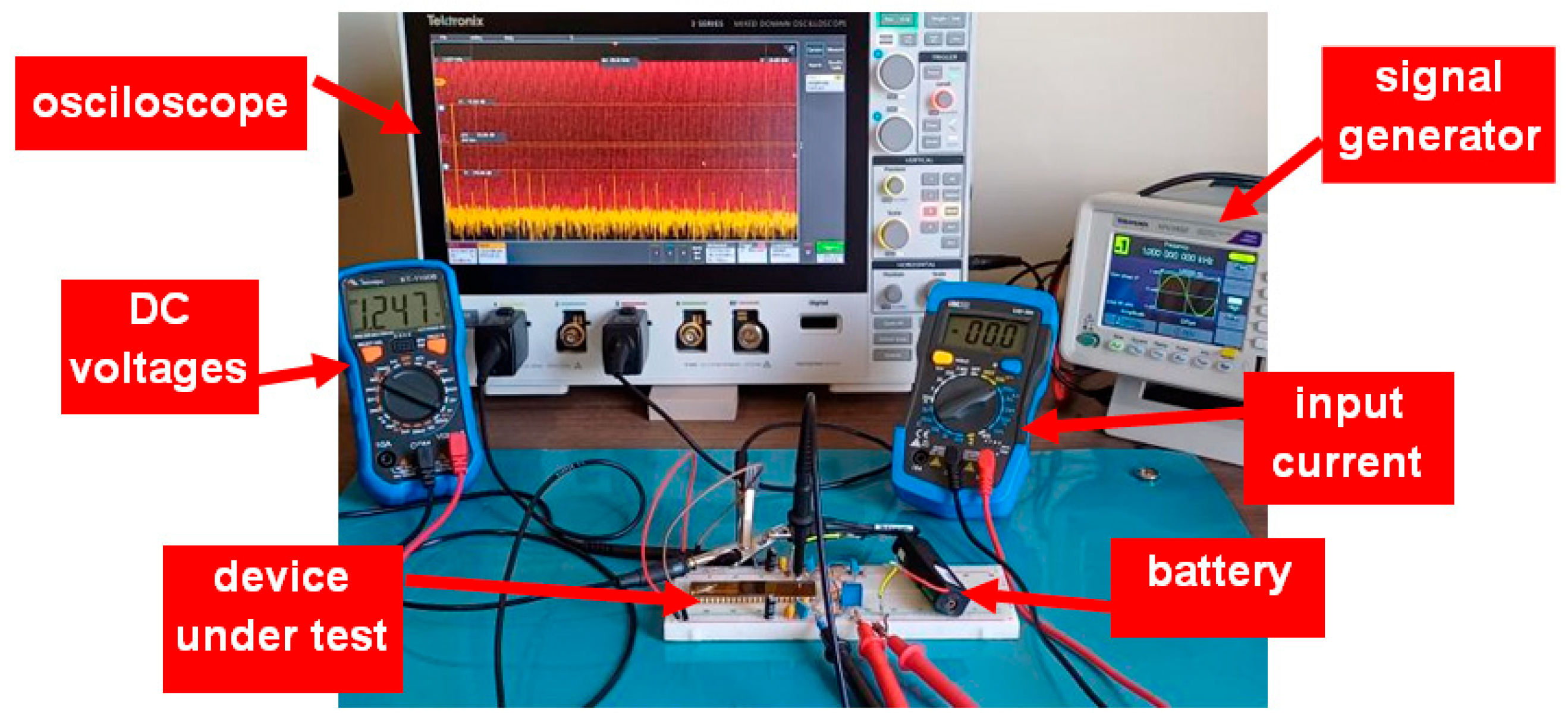
Figure 5 shows a photograph of the laboratory setup used during the experimental tests for measurements of the gain and noise of the LNA. The 1.2 V voltage supply is obtained by a battery to reduce the external interference. VCM is generated with the help of a potentiometer.

Figure 5.
Photograph of the experimental setup used to obtain the gain and noise characteristics of the LNA.
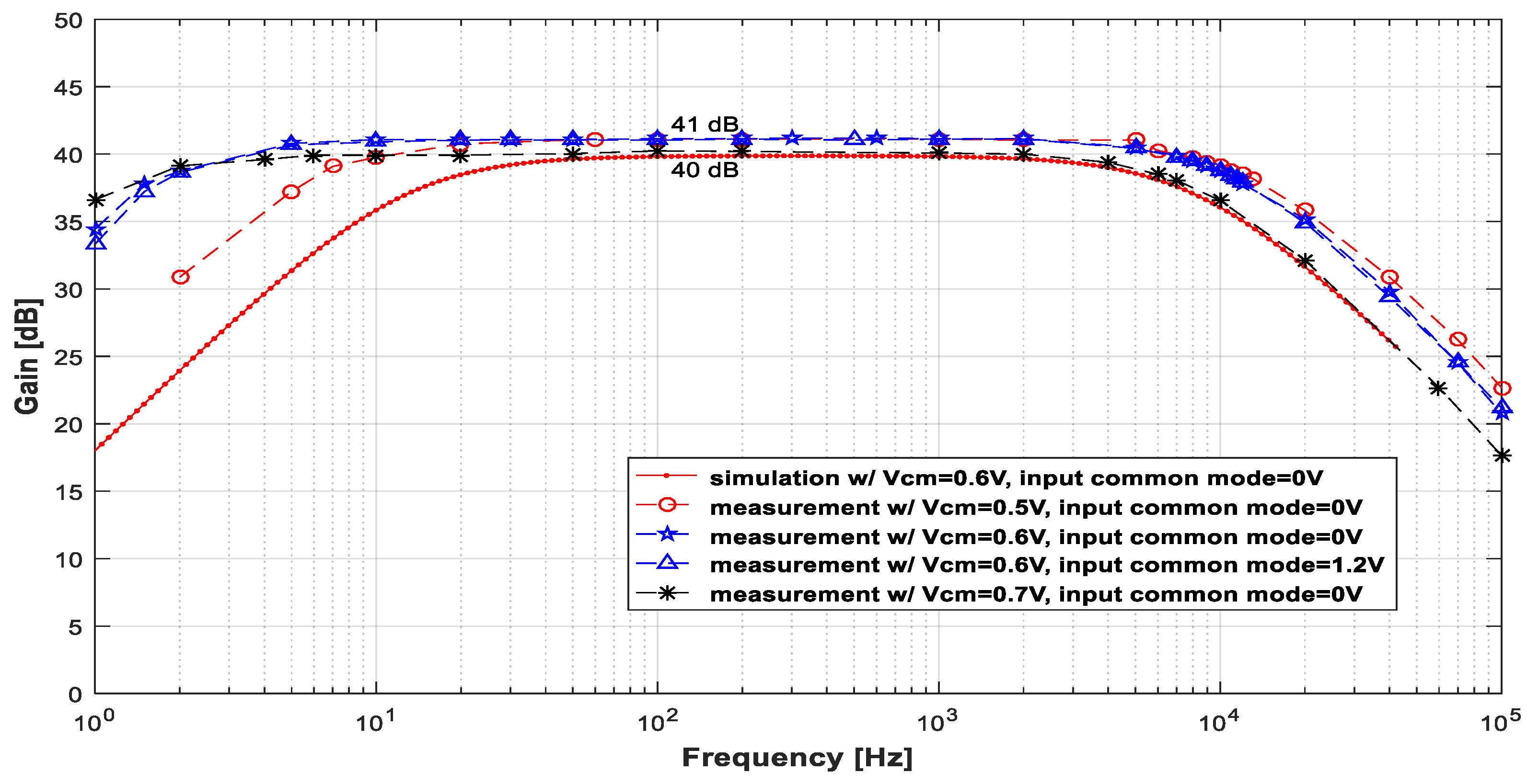
Figure 6 displays the measured gain × frequency curve for several common-mode voltages (VCM), different input common modes, and input signals with an amplitude of 2.2 mVpp. In this set of plots, the simulation results are also shown (dotted red line) to allow for comparisons. The measurements, in general, agree well with the simulation results. The most noticeable difference between the simulated and experimental results is the positions of the cutoff frequencies. The variation in these parameters is not surprising because fL depends on the pseudo-resistor, for which the value is difficult to estimate accurately, and fH depends on the transistors’ (M1 and M2’s) transconductance parameter (gm), which varies considerably in a process.

Figure 6.
Plots of the measured gain × frequency curves for input signals with an amplitude of 2 mVpp and several values of VCM and input common modes. These plots are compared with the simulations (dotted line in red).
Table 3 lists the measured common-mode voltage (VCM,out) at the output of the LNA, the maximum gain (Gmax), and the cutoff frequencies in terms of the common-mode voltage (VCM). The disparity between VCM,out and VCM arose because of the high-value pseudo-resistors and the gate leakage currents of M1 and M2.

Table 3.
Measured common-mode output voltage (VCM,out), maximum gain (Gmax), fL, and fH of the LNA for different VCMs values.
Notice that an elevation in the common-mode voltage (VCM), as depicted in Figure 6 and Table 3, leads to a decrease in both frequencies fL and fH. On the other hand, variations in VCM within the range of [0.5, 0.6] V did not yield significantly different gain curves. Additionally, variations in the input common mode did not alter the LNA operation. This demonstrates the robustness of the LNA concerning the input common mode, resulting in a low potential for the linear distortion of the signals during amplification.
The biasing voltage applied in the tests was VBIAS = 0.75 V, obtained using a bias resistance of RBIAS = 3.3 GΩ connected between the VBIAS node and the ground. This resulted in a total current of Itotal = 4.9 μA and a power consumption of 5.9 µW.
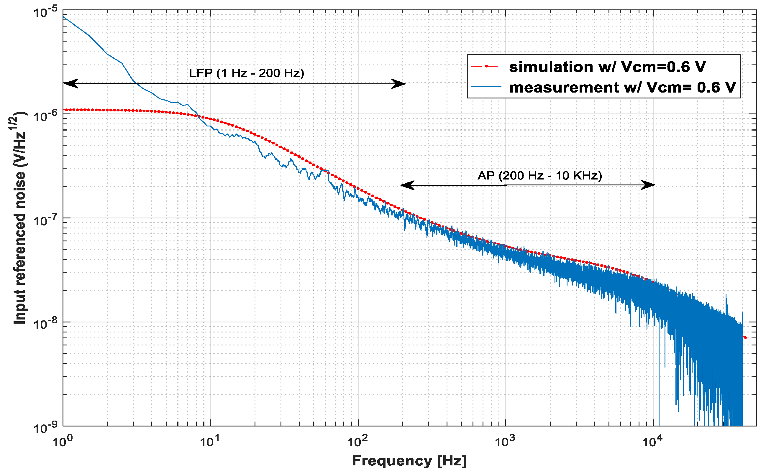
Figure 7 presents the measurement and simulation results of the input-referenced noise. The agreement between measurements and simulations is quite good for frequencies above 12 Hz, which is the low cutoff frequency found in the simulations. Below this frequency, the measured noise continues to increase because the cutoff frequency of the implemented LNA is at 1.5 Hz. The measured IRNs are 6.48 μVRMS from 1.5 Hz to 200 kHz, 3.45 μVRMS from 200 Hz to 11.5 kHz, and 7.36 μVRMS from 1.5 Hz to 11.5 kHz.
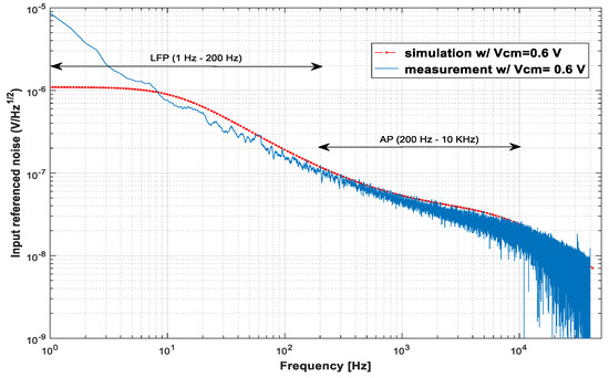
Figure 7.
Plots of the measured input-referenced noise × frequency for input signals with an amplitude of 2 mVpp (blue). These plots are compared with the simulations (dotted line in red).
In the LNA, the total harmonic distortion (THD) is less than −46 dB for input signals as high as 6.1 mVpp or less than −51 dB for input signals as high as 4.4 mVpp. The THD was calculated with the first nine harmonics.
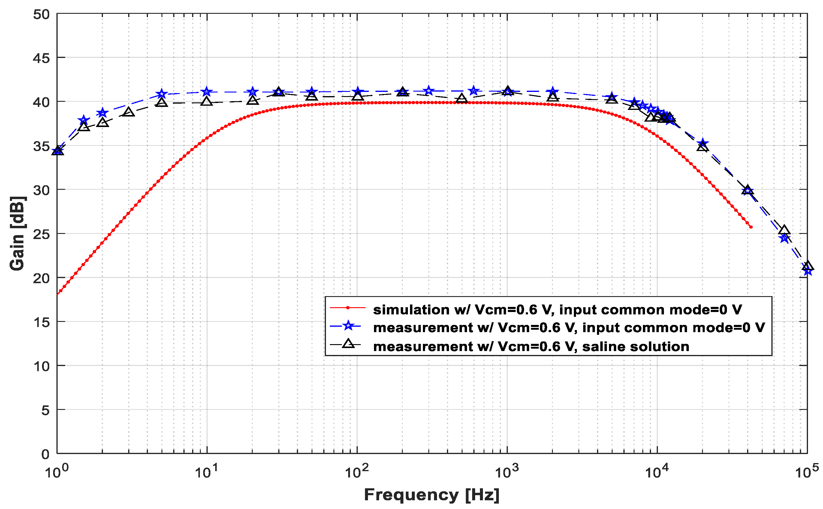
This LNA was also tested with a saline solution to emulate an ex vivo situation and evaluate its performance in real in vivo applications. Figure 8 presents the measured gains for signals injected into the saline solution. The amplitudes of the injected signals were adjusted to obtain approximately 5 mVpp at the LNA input. The voltage value of the generator output ranged between 6 mVpp and 20 mVpp, depending on the frequency.
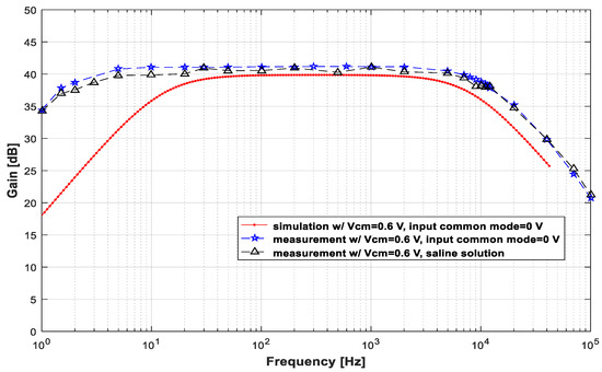
Figure 8.
Plot of the measured gain × frequency for signals injected into the saline solution. The signals injected into the solution were adjusted to obtain approximately 5 mVpp at the LNA input.
As seen in Figure 8, the gain did not show any appreciable reduction in the frequency range between 1 Hz and 100 kHz. In fact, it is possible to observe that the gain remained high, with its maximum value of 41.1 dB at 100 Hz.
3.2. Neurostimulator Circuit
The tests of this electronic block can be divided into static and dynamic tests. In static tests, the signals applied to the circuit do not change over time. On the contrary, in dynamic tests, the different signals vary over time. The experimental setups used for both types of tests are essentially the same, except for how the test signals were generated. The voltage (VBIAS) was set at 315 mV.
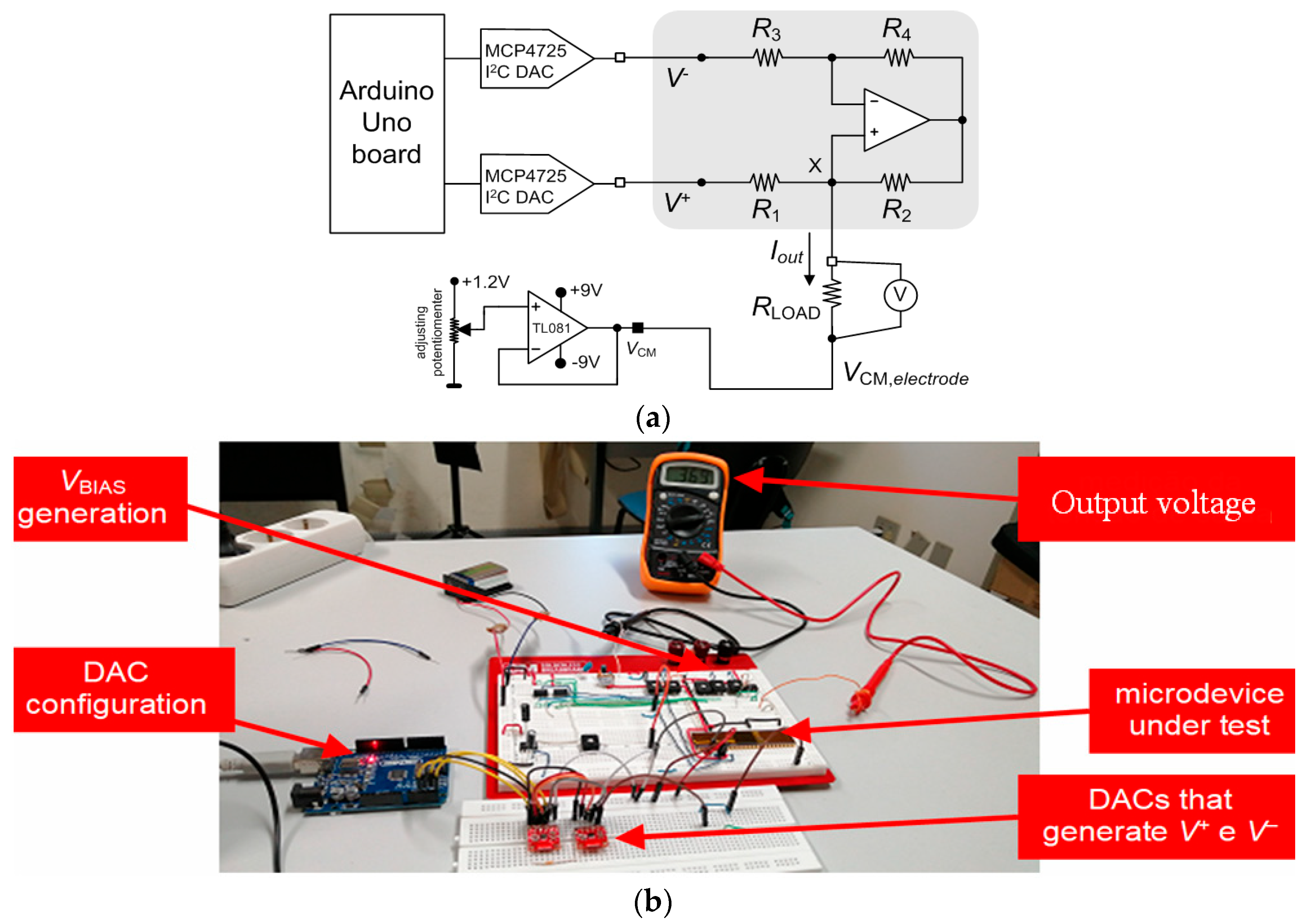
Figure 9a illustrates the schematic of the experimental setup for the static characterization of the neurostimulator circuit. This setup comprises a voltage follower, implemented with the operational amplifier (TL084), to generate the common-mode voltage (VCM,electrode) applied in the reference terminal of the electrode. The implantable electrode is represented by the load resistor (RLOAD).

Figure 9.
(a) Schematic of the experimental setup used in the static characterization of the neurostimulator circuit. (b) Photograph of the experimental setup used in the static characterization of the current pump.
The common-mode voltage (VCM,electrode) at the reference electrode was manually set between 0 V and 1.2 V in coarse steps of 0.3 V. Moreover, two breakout boards based on the MCP4725 digital-to-analog converter (DAC) with an I2C interface were used to make fine-tuning adjustments of the inputs (V+ and V−) and, thus, precise adjustments of the currents injected into the load resistor (RLOAD). An Arduino board was selected to control the DACs.
Figure 9b shows a photograph of the experimental setup used in the static characterization of the current pump.
Figure 10a illustrates the currents for the various combinations of the control and common-mode voltages {V+, V−, VCM,electrode} in “raw” form to allow for a clear and immediate visualization of the wide and quasi-symmetrical range of currents that are possible to generate with this current pump. In contrast, Figure 10b illustrates the currents parameterized in terms of the reference voltage of the electrode (VCM,electrode) and the inverting input voltage (V−). The output current was determined using the following expression:
A load resistance of RLOAD = 986.5 Ω was used for these tests. The output voltage (Vout) can range from 0 V to 1.2 V; therefore, the output current (Iout) can either be positive or negative, simply by making the voltage of the reference electrode (VCM,electrode) either equal to 0 V or 1.2 V, respectively. As it is possible to observe in Figure 10a,b, other intermediate currents are possible to be generated. The inversion of the current direction is mandatory in deep-brain stimulation applications.
The current pump was able to generate stimulation currents ranging from −325 μA to +318 μA. The path marked with the dashed yellow lines in Figure 10b illustrates how continuous current signals can be generated within this range.
For the dynamic tests, the frequency of the signal at V− is ten times higher than the frequency of the signal applied at V+. The amplitudes of both signals varied between 0 V and 1.2 V. These settings result in a wave, the product of the two input waves, with a sliced sine shape. The reference voltage (VCM,electrode) of the electrode was also manually adjusted between 0 V and 1.2 V during these tests. Figure 11 shows the experimental results of the dynamic characterization.
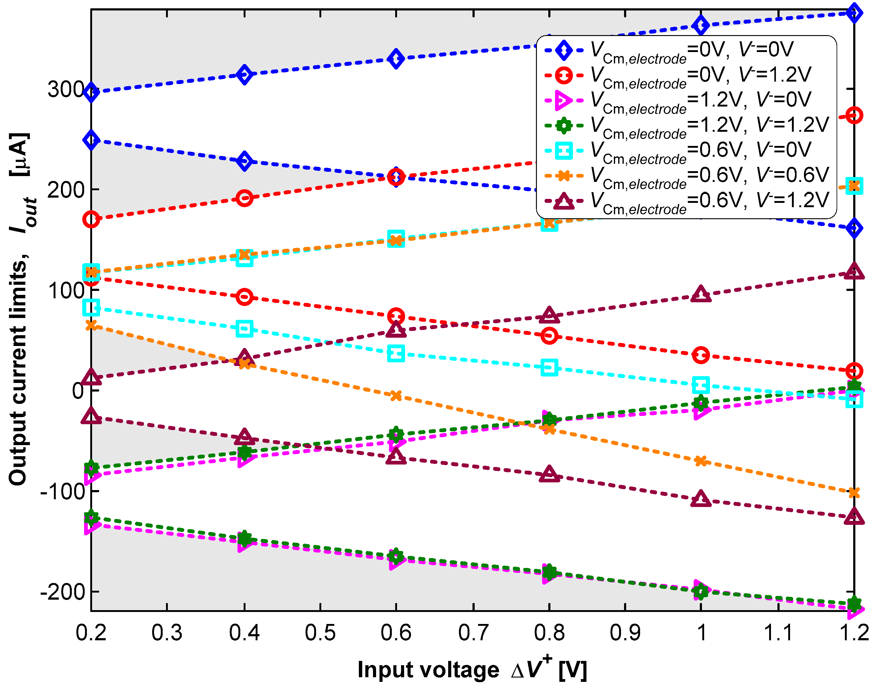
A set of sine waves with a common-mode voltage of 0.6 V and different amplitudes were applied in the non-inverting input (V+), with V− and VCM,electrode set at one of the voltages {0, 0.6, 1.2} V. The voltage difference (ΔV+) in the plot is the difference between the maximum and the minimum values of the voltage (V+). The voltage difference (ΔV+) is equal to 2A+ for a non-inverting input (V+) of V+ = 0.6 + A+.cos(2πft). The amplitude (ΔV+) was swept from 0.2 V to 1.2 V in steps of 0.2 V. The non-inverting input (V+) voltage variation is rail-to-rail for A+ = 0.6 V. Figure 11 also shows the results for seven combinations of {V−, VCM,electrode} in the set {0, 0.6, 1.2} V. Each combination defines the admissible range of the output current, for which plane domains are bounded above and below by two straight lines. The upper line occurs for V+ = 0.6 + ΔV+, while the bottom line occurs for V+ = 0.6 − ΔV+. It is possible to observe, in Figure 11, the ability to dynamically sweep the complete current limit, ranging from Imax = +375 μA to Imin = −218 μA, simply selecting the most suitable voltage combination of {V+, V−, VCM,electrode}.
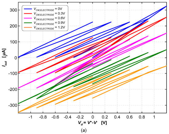
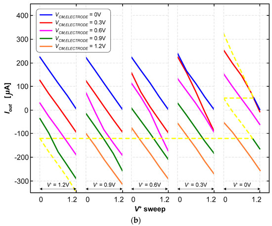
Figure 10.
(a) Stimulation currents for the various combinations of voltages, {V+, V−, VCM,electrode}, in “raw” form to allow for a clear and immediate visualization of the wide and quasi-symmetrical range of currents. (b) Stimulation currents are doubly parameterized in terms of the reference voltage of the electrode (VCM) and the inverting input (V−).


It is also possible to observe in Figure 11 that a limited set of voltage combinations of {V+, V−, VCM,electrode} must be avoided, under the penalty of not being able to generate very specific values of the electric current. These voltage combinations are associated with the “no-man’s land” regions marked with gray shading. These “no-man’s land” regions represent combinations that are not contained in the set of the seven planar domains for the different voltage combinations {V+, V−, VCM,electrode}.
The measurements showed that these results are valid for all the voltage combinations {V+, V−, VCM,electrode} for a frequency of up to f−3dB = 1.5 MHz. This frequency is the one that narrows the current range from Imax − Imin to −3 dB. For example, the measurements indicated that Imax = +297 μA and Imin = +248.4 μA for V+ = 0.6 + 0.1cos(2πft) or ΔV+ = 0.2 V, with f < f−3dB/10, V− = 0 V, and VCM,electrode = 0 V. This results in ΔIout = Imax − Imin = +49 μA. The measurements also showed that ΔIout = (+49) × (2)−1/2 × (10−6) = +34.6 μA for f = f−3dB = 1.5 MHz.
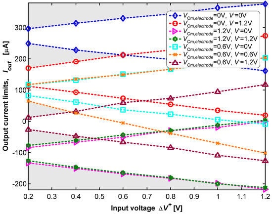
Figure 11.
Dynamic characterization using sine waves with rail-to-rail amplitudes.
Figure 11.
Dynamic characterization using sine waves with rail-to-rail amplitudes.
4. Discussion
The LNA and neurostimulator were designed and fabricated in the CMOS (65 nm) from TSMC. Table 4 compares the LNA with a few related key works found in the literature [9,10,21,22,23,26,27,28,29,30,31]. The figure-of-merit (FOM) was calculated to better rank and compare this work with the others with respect to the internal noise–power consumption tradeoff. The FOM applied here is the noise efficiency factor (NEF), introduced in 1987 by Steyaert et al. [32] and widely used since then. It is given as follows:
where Itotal is the total current absorbed by the amplifier stage (This current excludes the amount absorbed by the bias stage.); UT is the thermal voltage, given by kT/q (≈26 mV at a room temperature of 300 K); k is the Boltzmann constant; T is the room temperature, expressed in Kelvin; IRN is the total RMS input-referred noise; and BW is the LNA bandwidth.

Table 4.
Comparison of the proposed LNA with state-of-the-art LNAs.
It must be noted that this FOM compares the noise–power tradeoff with that of a single ideal bipolar transistor. The lower the FOM, the better will be the LNA in relation to the global noise performance.
Two important observations must be made regarding the results presented in Table 4: four of the five circuits with the lowest NEFs [10,22,27,31] use single-input CMOS-inverter-based LNAs in the first gain stage. The inverter introduced half the amount of power noise. Consequently, the NEF is reduced by ; implementations with processes with higher minimum lengths [11,26,27,28,29,30,31] display better NEFs.
The LNA presented in this work exhibits an NEF for AP applications that is comparable to the best results found in the literature. This result is attained partly because of the sizing and optimization process performed through the application of metaheuristics.
Table 5 compares the features of the neurostimulator circuit with a few related key works found in the literature [33,34,35,36,37,38,39]. All the works listed in Table 5 were implemented using CMOS components. The neurostimulator presented in this paper allows for the generation of current signals with non-standard waveforms and is suitable for delayed feedback, a characteristic shared only by the neurostimulator presented in [37]. It also enables the generation of bipolar current pulses, a characteristic shared by [32,35], and provides the best current range for the lowest power supply voltage, with a ratio of 535.8 μA/V (The second-best result is presented by [36], with a ratio of 412.5 μA/V). In general, all the neurostimulators presented in this paper comply with the minimum pulse duration of 90 μs and the frequency of 130 Hz required by DBS applications.

Table 5.
Comparison of the proposed neurostimulator with state-of-the-art neurostimulators.
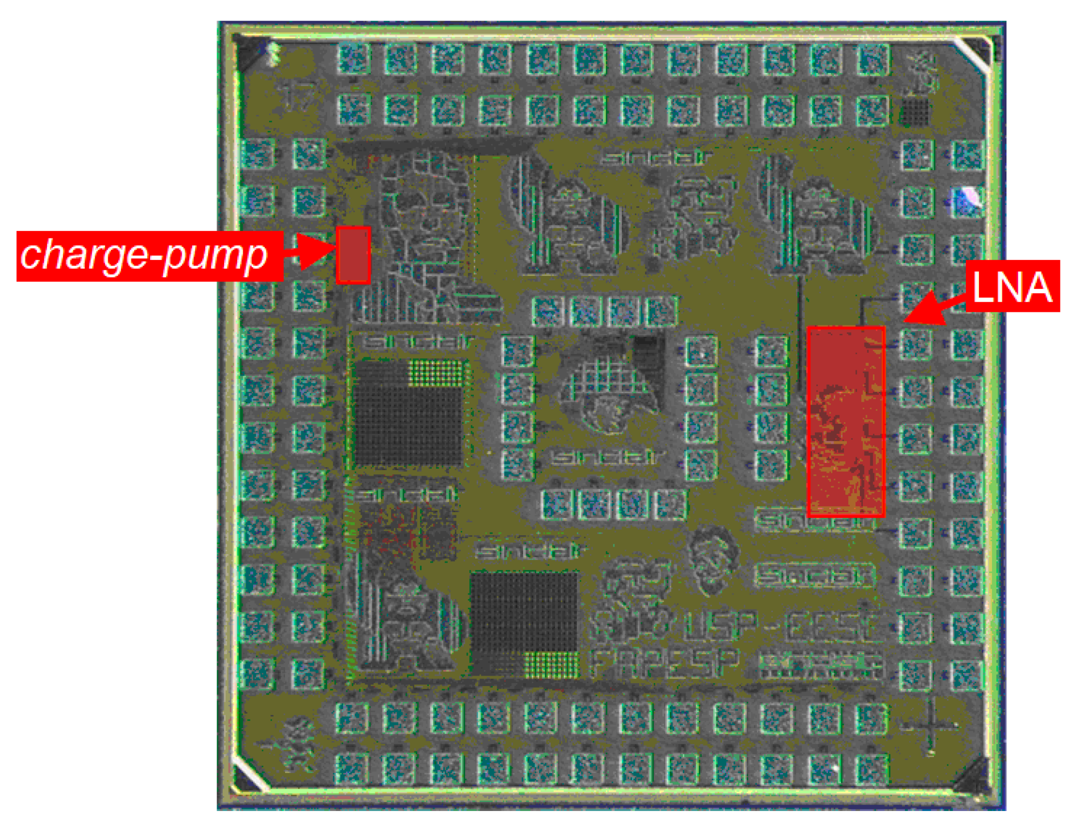
To conclude, Figure 12 depicts a photograph of the fabricated CMOS integrated circuit housing both the LNA and the neurostimulator, which occupies 1.8 mm × 1.8 mm of area. The figure emphasizes the two circuits presented in this paper.
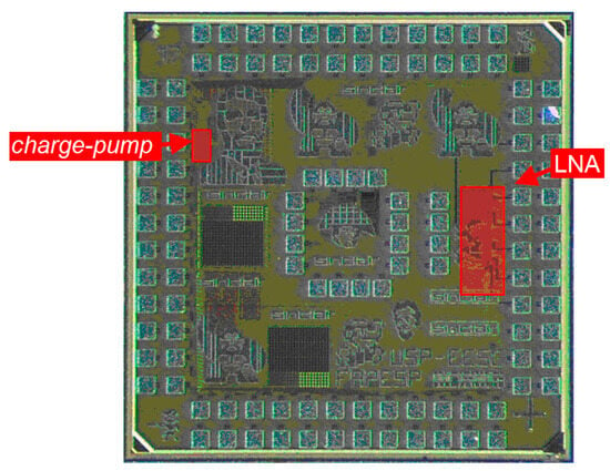
Figure 12.
Photograph of the fabricated CMOS microdevice (1.8 mm × 1.8 mm), with emphasis on the LNA and the current pump presented in the paper.
5. Conclusions
Deep-brain stimulation (DBS) stands as a remarkably effective medical treatment, significantly enhancing the quality of life for patients. Closed-loop deep-brain stimulation (CLDBS) further elevates this treatment by automatically adapting the stimulation parameters. This paper presents the implementation of two crucial circuits for CLDBS, the low-noise amplifier (LNA) and the neurostimulator, both fabricated using a 65 nm CMOS process. The implemented LNA presents an NEF for AP signals, ranging from 20 Hz to 11.5 kHz, compatible with the performance of the best circuits in the literature (NEF = 2.63). Moreover, its total noise from 1.5 Hz to 11.5 kHz is 7.36 μVrms, which is below the levels of thermal and biological noises. This feature made it suitable for applications involving both LFP and AP signals. The implemented neurostimulator provides biphasic current pulses with non-standard waveforms and is suitable for delayed feedback.
Author Contributions
Conceptualization, T.M.N., R.G., J.N.S.J. and J.P.C.; methodology, T.M.N., R.G., J.N.S.J. and J.P.C.; validation, T.M.N., M.L.M.A. and R.G.; writing—original draft preparation, T.M.N., R.G. and M.L.M.A.; writing—final revision, M.L., J.N.S.J., V.M., J.A.A., J.L.A. and J.P.C.; supervision, E.T.F. and E.C.; project administration, M.L., J.N.S.J., J.A.A., V.M., J.L.A. and J.P.C.; funding acquisition, M.L., J.N.S.J., J.A.A., V.M., J.L.A. and J.P.C. All authors have read and agreed to the published version of the manuscript.
Funding
This work was partially supported by the FAPESP agency (Fundação de Amparo à Pesquisa do Estado de São Paulo) through the project with the reference 2019/05248-7, and by the CNPq (Conselho Nacional de Desenvolvimento Cientifico e Tecnológico) through the project with the reference 402752/2023-6. Professor João Paulo Carmo was supported by a PQ scholarship with the reference CNPq 305858/2023-8.
Data Availability Statement
The data that support the findings of this study are available from the corresponding author upon reasonable request.
Conflicts of Interest
The authors declare no conflicts of interest.
References
- Appleby, B.S.; Duggan, P.S.; Regenberg, A.; Rabins, P.V. Psychiatric and neuropsychiatric adverse events associated with deep brain stimulation: A meta-analysis of ten years’ experience. Mov. Disord. 2007, 22, 1722–1728. [Google Scholar] [CrossRef] [PubMed]
- Hickey, P.; Stacy, M. Deep Brain Stimulation: A Paradigm Shifting Approach to Treat Parkinson’s Disease. Front. Neurosci. 2016, 10, 173. [Google Scholar] [CrossRef] [PubMed]
- Hoang, K.B.; Cassar, I.R.; Grill, W.M.; Turner, D.A. Biomarkers and Stimulation Algorithms for Adaptive Brain Stimulation. Front. Neurosci. 2017, 11, 303295. [Google Scholar] [CrossRef] [PubMed]
- Fins, J.J. Chapter 9: Deep Brain Stimulation: Ethical Issues in Clinical Practice and Neurosurgical Research; Neuromodulation; Academic Press: Cambridge, MA, USA, 2009; pp. 81–91. [Google Scholar]
- Faraji, B.; Rouhollahi, K.; Nezhadi, A.; Jamalpoor, Z. A Novel Closed-Loop Deep Brain Stimulation Technique for Parkinson’s Patients Rehabilitation Utilizing Machine Learning. IEEE Sens. J. 2023, 23, 2914–2921. [Google Scholar] [CrossRef]
- Parastarfeizabadi, M.; Kouzan, A.Z. A Miniature Low-Power Multi-Biomarker-Based Brain Sensor for Closed-Loop DBS. IEEE Sens. J. 2017, 17, 3109–3115. [Google Scholar] [CrossRef]
- Holleman, J.; Zhang, F.; Otis, B. Ultra-Low-Power Integrated Circuit Design for Wireless Neural Interface; Springer: New York, NY, USA, 2011. [Google Scholar]
- Chang, S.-I.; Park, S.-Y.; Yoon, E. Low-Power Low-Noise Pseudo-Open-Loop Preamplifier for Neural Interfaces. IEEE Sens. J. 2017, 17, 4843–4852. [Google Scholar] [CrossRef]
- Yang, T.; Holleman, J. An ultralow-power low-noise CMOS biopotential amplifier for neural recording. IEEE Trans. Circuits Syst. II Exp. Briefs. 2015, 62, 927–931. [Google Scholar] [CrossRef]
- Harrison, R.R.; Charles, C. A low-power low-noise CMOS for amplifier neural recording applications. IEEE J. Solid-State Circuits 2003, 38, 958–965. [Google Scholar] [CrossRef]
- Kárász, Z.; Fiáth, R.; Földesy, P.; Vázquez, A.R. Tunable Low Noise Amplifier Implementation with Low Distortion Pseudo-Resistance for in Vivo Brain Activity Measurement. IEEE Sens. J. 2013, 14, 1357–1363. [Google Scholar] [CrossRef]
- Riem, R.; Raman, J.; Borgmans, J.; Rombouts, P. A Low-Noise Instrumentation Amplifier with Built-in Anti-Aliasing for Hall Sensors. IEEE Sens. J. 2021, 21, 18932–18944. [Google Scholar] [CrossRef]
- Nordi, T.M.; Gounella, R.H.; Luppe, M.; Junior, J.N.S.; Fonoff, E.T.; Colombari, E.; Romero, M.A.; Carmo, J.P. Low-Noise Amplifier for Deep brain Stimulation (DBS). Electronics 2022, 11, 939. [Google Scholar] [CrossRef]
- Ha, S.; Kim, C.; Mercier, P.P.; Cauwenberghs, G. High-Density Integrated Electrocortical Neuronal Interface; Academic Press: London, UK, 2019. [Google Scholar]
- Wattanapanitch, W.; Fee, M.; Sarpeshkar, R. An Energy-Efficient Micropower Neural Recording Amplifier. IEEE Trans. Biomed. Circuits Syst. 2007, 1, 136–147. [Google Scholar] [CrossRef] [PubMed]
- Kassiri, H.; Abdelhalim, K.; Genov, R. Low-distortion super-GOhm subthreshold-MOS resistors for CMOS neural amplifiers. In Proceedings of the 2013 IEEE Biomedical Circuits and Systems Conference (BioCAS), Rotterdam, The Netherlands, 31 October–2 November 2013; pp. 270–273. [Google Scholar]
- Clerc, M.; Kennedy, J. The particle swarm–explosion, stability, and convergence in a multimensional complex space. Trans. Evol. Comput. 2002, 6, 58–73. [Google Scholar] [CrossRef]
- Weber, T.O.; Noije, W.A.M.V. Design of analog circuits using simulated annealing/quenching with crossovers and particle swarm optimization. In Simulating Annealing–Advances, Application and Hybridizations; Tuzuki, M.S.G., Ed.; IntechOpen: London, UK, 2012; pp. 219–244. [Google Scholar]
- Ishibe, E.I.; Soares, J.N. A CMOS bandgap reference circuit with a temperature coefficient adjustment block. In Proceedings of the 26th Symposium on Integrated Circuits and Systems Design (SBCCI), Curitiba, Brazil, 2–6 September 2013; pp. 1–6. [Google Scholar]
- Navarro, J.; Luppe, M. Performance Comparison of High-Speed Dual Modulus Prescalers Using Metaheuristic Sizing/Optimization. In Proceedings of the 33rd Symposium on Integrated Circuits and Systems Design (SBCCI), Campinas, Brazil, 24 September–28 August 2020; pp. 1–6. [Google Scholar]
- Chandrakumar, H.; Marković, D. An 80-mVpp linear-input range, 1.6-GΩ input impedance, low-power chopper amplifier for closed-loop neural recording that is tolerant to 650-mVpp common-mode interference. IEEE J. Solid-State Circuits 2017, 52, 2811–2828. [Google Scholar] [CrossRef]
- Ng, K.A.; Xu, Y.P. A multi-channel neural-recording amplifier system with 90 dB CMRR employing CMOS-inverter-based OTAs with CMFB through supply rails in 65 nm CMOS. In Proceedings of the 2015 IEEE International Solid-State Circuits Conference (ISSCC) Digest of Technical Papers, San Francisco, CA, USA, 22–26 February 2015; pp. 1–3. [Google Scholar]
- Biederman, W.; Yeager, D.J.; Narevsky, N.; Koralek, A.C.; Carmena, J.M.; Alon, E.; Rabaey, J.M. A Fully-Integrated, Miniaturized (0.125 mm2) 10.5 μW Wireless Neural Sensor. IEEE J. Solid-State Circuits 2013, 48, 960–970. [Google Scholar] [CrossRef]
- Kölbl, F.; N’Kaoua, G.; Naudet, F.; Berthier, F.; Faggiani, E.; Renaud, S.; Benazzouz, A.; Lewis, N. An Embedded Deep Brain Stimulator for Biphasic Chronic Experiments in Freely Moving Rodents. IEEE Trans. Biomed. Circuits Syst. 2016, 10, 72–78. [Google Scholar] [CrossRef] [PubMed]
- AN-1515; A Comprehensive Study of the Howland Current Pump. Texas Instruments: Dallas, TX, USA, 26 April 2013.
- Muller, R.; Le, H.-P.; Li, W.; Ledochowitsch, P.; Gambini, S.; Bjorninen, T.; Koralek, A.; Carmena, J.M.; Maharbiz, M.M.; Alon, E.; et al. A minimally invasive 64-channel wireless µECoG implant. IEEE J. Solid-State Circuits. 2015, 50, 344–359. [Google Scholar] [CrossRef]
- Zhang, F.; Holleman, J.; Otis, B.P. Design of Ultra-Low Power Biopotential Amplifier for Biosignal Acquisition Application. IEEE Trans. Biomed. Circuits Syst. 2012, 6, 244–355. [Google Scholar] [CrossRef] [PubMed]
- Kim, H.-J.; Park, Y.; Eom, K.; Park, S.-Y. An Area- and Energy-Efficient 16-Channel, AC-Coupled Neural Recording Analog Frontend for High-Density Multichannel Neural Recordings. Electronics 2021, 10, 1972. [Google Scholar] [CrossRef]
- Kwak, J.Y.; Park, S.-Y. Compact Continuous Time Common-Mode Feedback Circuit for Low-Power, Area-Constrained Neural Recording Amplifiers. Electronics 2021, 10, 145. [Google Scholar] [CrossRef]
- Tasneem, N.T.; Mahbub, I. A 2.53 NEF 8-bit 10 kS/s 0.5 μm CMOS Neural Recording Read-Out Circuit with High Linearity for Neuromodulation Implants. Electronics 2021, 10, 590. [Google Scholar] [CrossRef]
- Holleman, J.; Otis, B. A Sub-Microwatt Low-Noise Amplifier for Neuronal Recording. In Proceedings of the 29th Annual International Conference IEEE EMBS, Lyon, France, 23–26 August 2007; pp. 3930–3933. [Google Scholar]
- Steyaert, M.S.; Sansen, W.M. A micropower low-noise monolithic instrumentation amplifier for medical purposes. IEEE J. Solid State Circuits 1987, 22, 1163–1168. [Google Scholar] [CrossRef]
- Pinnell, R.C.; de Vasconcelos, A.P.; Cassel, J.C.; Hofmann, U.G. A miniaturized programmable Deep brain stimulator for group-housing and water maze use. Front. Neurosci. 2018, 12, 353871. [Google Scholar] [CrossRef] [PubMed]
- Ewing, S.G.; Lipski, W.J.; Grace, A.A.; Winter, C. An inexpensive charge-balanced rodent deep brain stimulation device a step-by-step guide to its procurement and construction. J. Neurosci. Methods 2013, 219, 324–330. [Google Scholar] [CrossRef]
- Kouzani, A.Z.; Abulseoud, O.A.; Tye, S.J.; Hosain, M.D.K.; Berk, M. A low power micro deep brain stimulation device for murine preclinical research. IEEE J. Transl. Eng. Health Med. 2013, 1, 1500109. [Google Scholar] [CrossRef]
- Pinnell, R.C.; Dempster, J.; Pratt, J. Miniature wireless recording and stimulation system for rodent behavioral testing. J. Neural Eng. 2015, 12, 066015. [Google Scholar] [CrossRef] [PubMed]
- Adams, S.D.; Bennet, K.E.; Tye, S.J.; Berk, M.; Kouzani, A.Z. Development of a miniature device for emerging deep brain stimulation paradigms. PLoS ONE 2019, 14, e0212554. [Google Scholar] [CrossRef] [PubMed]
- Tibara, H.; Naudeta, F.; Kölblc, F.; Ribota, B.; Faggiania, E.; N’Kaouac, G.; Renaudc, S.; Lewisc, N.; Benazzouza, A. In vivo validation of a new portable stimulator for chronic deep brain stimulation in freely moving rats. J. Neurosci. Methods 2020, 333, 108577. [Google Scholar] [CrossRef]
- Fluri, F.; Mützel, T.; Schuhmann, M.K.; Krstić, M.; Endres, H.; Volkmann, J. Development of a head-mounted wireless microstimulator for deep brain stimulation in rats. J. Neurosci. Methods 2017, 291, 249–256. [Google Scholar] [CrossRef]
Disclaimer/Publisher’s Note: The statements, opinions and data contained in all publications are solely those of the individual author(s) and contributor(s) and not of MDPI and/or the editor(s). MDPI and/or the editor(s) disclaim responsibility for any injury to people or property resulting from any ideas, methods, instructions or products referred to in the content. |
© 2024 by the authors. Licensee MDPI, Basel, Switzerland. This article is an open access article distributed under the terms and conditions of the Creative Commons Attribution (CC BY) license (https://creativecommons.org/licenses/by/4.0/).

