Abstract
This research sought to determine the optimal conditions for depositing thin silver layers in the fabrication of low-emissivity coatings. The study utilized an in-line semi-industrial high-vacuum magnetron sputtering system with rectangular targets, closely resembling those used in industrial settings. Trilayer AZO/Ag/AZO structures were deposited to enhance the wetting properties of the silver, and to protect it from the atmosphere. The effects of the power and argon flow on the sample properties were analyzed, along with variations in the silver thickness. The results demonstrate that a lower power (200 W) and higher argon flows (1000 sccm) lead to a higher transmittance and a lower sheet resistance, resulting in a reduced emissivity (up to 0.015 for 24 nm of silver). The identified optimal conditions offer valuable recommendations for producing more efficient and optically superior coatings. This study also reveals the importance of the silver thickness to the properties of the coatings, in accordance with previous research findings. These findings provide insights for improving the performance of low-emissivity coatings in various applications.
1. Introduction
Low-emissivity coatings are widely used in building construction, to enhance the energy efficiency of structures [1]. These coatings are designed with a fundamental principle in mind: they remain transparent within the visible spectrum, while exhibiting a high reflectivity in the near- and mid-infrared regions. A high transparency within the visible range is crucial, as it allows natural light to penetrate into the building’s interior. Simultaneously, the high reflectivity in the infrared spectrum serves two key purposes [2]. Firstly, in warmer climates, it is essential that the glazing reflect the infrared portion of the solar spectrum, minimizing solar radiation within the building. On the other hand, the glazing requires a high thermal infrared reflectance to ensure that the coating is low-emissive and insulates the interior of the building from energy transfer via radiation [3].
This type of coating typically consists of thin layers of transparent oxides or nitrides, combined with thin layers of a noble metal, such as gold, silver, or copper [4,5,6]. Silver is the most commonly used noble metal, due to its more suitable optical properties [7,8], which allow the coatings to remain transparent in the visible range, while achieving a high infrared reflectance. The transparent thin layers are essential for adjusting the optical properties (often acting as an anti-reflective effect, to maximize visible transmission), but they also serve other functions, such as acting as a seed layer to improve silver deposition and enhance adhesion, or protecting the silver layer from exposure to the atmosphere [9,10,11,12,13].
A wide variety of materials, such as SnO2 [14,15], ZnO [4], Si3N4 [16], TiO2 [17], AlN [18,19], AZO [20], and ITO [21,22], can be used as transparent materials to adjust the optical properties. Among them, AZO yields particularly favorable results, as it exhibits a good wetting behavior in the silver, and forms more uniform silver layers [23,24]. AZO/Ag/AZO structures have been extensively studied, due to their significance as low-emissivity coatings, for the fabrication of transparent and conductive surfaces with a low sheet resistance [20,25,26,27,28,29].
The silver deposition conditions can significantly impact the properties of the coating, and determine its overall quality [30]. In [23], the researchers focus on examining the effect of the applied power on the quality of the silver film; however, the analysis is limited to only four samples deposited at different power levels. The observed variations in optical and electrical properties may not solely be attributed to the applied power, as the differences in the thickness of the deposited silver have not been considered. Previous research has explored the influence of the substrate temperature on the silver properties [31], while, in [32], the effect of the thickness was investigated.
This study aims to investigate the effect of modifying silver deposition parameters, to achieve optimal values for transparency and sheet resistance (related to the coating’s emissivity) in AZO/Ag/AZO structures. Specifically, an examination of optical and electrical properties has been conducted, through varying the pressure and working power to create the most transparent and conductive silver coatings. The potential thickness change is an essential consideration when altering the deposition conditions, and great care has been taken in this study to ensure that the samples are entirely comparable. This is a crucial aspect that has received less attention in previous studies. In this work, an adjustment is performed based on the deposited silver thickness, which serves to compare the quality of the silver coatings, even if they have a different transmittance and sheet resistance. Moreover, this research was conducted using an in-line sputter system for large area deposition with linear magnetron sources, enabling the extrapolation of the results to industrial-scale installations. These findings could also be beneficial for the production of transparent and conductive coatings based on thin silver layers, which can be useful in solar cells or electrooptic devices.
2. Materials and Methods
The AZO/Ag/AZO thin-film structure was primarily deposited onto microscope slides using a semi-industrial high-vacuum magnetron sputtering system, employing the DC pulsed technique, with rectangular 600 mm × 100 mm targets. Additionally, the latest samples were deposited on glass substrates with a thickness of 4 mm. The employed sputtering system closely resembles those used in industrial settings (an in-line sputter system), enabling the reliable extrapolation of results to large-scale installations. The silver target exhibited a purity of 99.9%, while the AZO target (zinc oxide doped with 2 wt% aluminum oxide) exhibited a purity of 99.95%. After a base pressure of the order of 10−5 Pa was achieved in the process chamber, an argon flow was introduced, to establish an inert atmosphere. Prior to deposition, the substrates were thoroughly cleaned with detergent (ACEDET 5509, Aachener Chemische Werke, Mönchengladbach, Germany), and an ion gun was employed, to eliminate any potential surface contaminants. This was achieved with an argon flow rate of 50 sccm, and an acceleration voltage of 2000 V.
The thickness of each material (AZO and silver) at specific conditions has been related to the carrier speed using a mechanical profilometer model DekTak XT (Bruker, Billerica, MA, USA), which has a vertical resolution of 0.1 nm, and a typical error of approximately 1 nm. The carrier speed is controlled using stepper motors, and can be adjusted between 0.21 and 42.00 mm/s.
Transmittance and reflectance spectra were obtained using a Vis–NIR spectrophotometer and a mid-infrared range spectrometer. The first device had a measurement range between 300 and 2500 nm using the standard EN 410:2011 [33]; the second was an FT-IR Perkin-Elmer Spectrum 100 (PerkinElmer, Waltham, MA, USA), which measures between 200 and 4000 cm−1 (2.5–50 μm), with a step of 2 cm−1 and a resolution of 16 cm−1.
One property used to characterize the coatings is the visible transmittance factor, which is calculated according to the standard EN 410:2011, using the following expression:
where T(λ) is the spectral transmittance factor of the sample, S(λ) is the spectral distribution of the illuminant, and V(λ) is the spectral sensitivity of the human eye [34]. D65 is used as the illuminant, as it is commonly used in building construction [34].
The emissivity (ε) is related to the reflectance (ρn,IR), with the following equation:
where the reflectance ρn,IR is calculated according to the standard EN 12898:2019 [35].
An alternative estimation of emissivity can be obtained based on the sheet resistance (Rs), measured in Ω/□ [29]. This is a measure of how much a thin conductive film resists the flow of electrical current per unit square area. The sheet resistance was measured with a four-point probe JANDEL RM3000 model. The relationship between both parameters is as follows:
This was the predominant method used throughout this study.
3. Results and Discussion
The main objective of this research was to study the optimal deposition conditions for thin silver layers for use in low-emissivity coatings. The goal was to determine which conditions provide samples with the maximum transparency and conductivity. The results of this optimization are also of interest for obtaining transparent and conductive electrical contacts.
3.1. Calibration
For the establishment of a relationship between the carrier speed and the deposited thickness for a given material under specific conditions, single-layer samples were prepared for each material, and measurements were taken using the profilometer, to obtain the parameters shown in Table 1.

Table 1.
The deposition conditions and values obtained at each calibration. The dynamic deposition rate is the product of the carrier speed multiplied by the thickness.
Once the dynamic deposition rate has been determined, it becomes feasible to deposit samples with varying thicknesses, given that the deposited thickness is directly proportional to the dynamic deposition rate, and inversely proportional to the carriage speed. Furthermore, as a preliminary approach to determine the dynamic deposition rate at other power levels, the dynamic deposition rate is considered to be proportional to the power.
The deposition conditions of AZO were maintained at the calibrated values, to avoid introducing parameters unrelated to the silver deposition. For the specific equipment used, 2000 W corresponds to a power density of 3.33 W/cm2, and a flow rate of 300 sccm results in a pressure of approximately 2 × 10⁻¹ Pa. Based on this calibration, we can ascertain the dynamic deposition rate (carrier speed·thickness) of each material under specific conditions. By manipulating the carriage speed, we can precisely regulate the thickness of the deposited layer. This is because the deposited thickness is inversely proportional to the carriage speed; for instance, if we were to double the carriage speed, the deposited thickness would be halved, as the sample would be exposed for only half the duration. Layers of 10 nm of AZO were deposited on both sides of the silver layers. However, the final set of samples involved specific variations in which this deposition thickness was not used. The bottom layer enhances the adhesion and wetting of the silver, while the top layer protects it from atmospheric exposure, and prevents rapid degradation.
3.2. Flow and Power Variation
Next, the impact of varying deposition power and argon flow on the silver deposition process was investigated. To achieve this, the rest of the conditions were kept constant, except for the carrier speed, which was proportionally adjusted according to the power to maintain a similar deposited thickness.
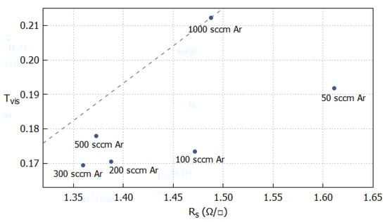
For the first series, the power was set at 500 W, and various argon flows were injected. The transmission spectra can be observed in Figure 1a. As shown, there was relatively little variation in the transmittance obtained in the spectra. However, a slight but clear improvement was observed between certain samples, indicating that this variation was not merely noise, but rather a discernible trend. Using Equation (1), the factor Tvis of each sample can be obtained; in Figure 1b, this factor is plotted against the sheet resistance (Rs). The measured sheet resistance corresponds to the AZO/Ag/AZO multilayer. However, as the AZO layers were not deposited under optimal conditions for high conductivity (their main role is to enhance wettability and adhesion, and provide protection to the silver layer), the conductivity of silver significantly surpassed that of AZO. Consequently, the primary determinant of the sheet resistance value was the silver layer.
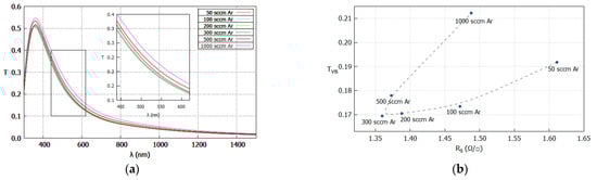
Figure 1.
Series at 500 W and various flows for AZO (10 nm)/Ag (25 nm)/AZO (10 nm): (a) transmittance spectrum in the visible and near-infrared range; (b) visible transmittance factor against sheet resistance.
At a flow rate of 300 sccm, the sample exhibits the lowest resistance, indicating the least emissivity. Lower flow rates result in a higher resistance, likely due to the limited number of argon atoms impacting the target; this leads to fewer sputtered silver atoms and a slower deposition rate. Conversely, higher flow rates also yield higher resistance. This behavior can be attributed to the gas density of argon atoms, which reduces the mean free path of the silver atoms, causing more frequent collisions before the substrate is reached.
As we aim to obtain samples with the highest transparency and the lowest emissivity (lower Rs), the optimal sample would be the one shown in the upper-left corner of Figure 2. Hence, low flow rates are discarded (<300 sccm). However, as the sample at 1000 sccm has a higher transmittance, and the samples at 500 and 300 sccm have a lower sheet resistance (indicative of a lower emissivity), we cannot determine a clear preference for a specific flow rate at this stage.
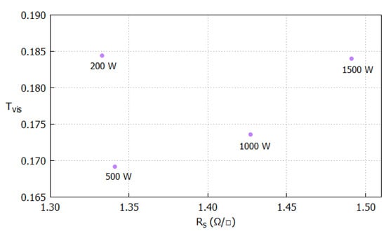
Figure 2.
A 300 sccm argon flow (fixed). Visible transmittance factor against sheet resistance in the AZO (10 nm)/Ag (24 nm)/AZO (10 nm) structure.
To analyze how the power affects the results, the argon flow was fixed at 300 sccm, and different samples were obtained in the 200–1500 W range. Analogously to the previous cases, Tvis was obtained from the spectra, and is represented in Figure 2.
In this case, the sample with 200 W has the highest transmittance and the lowest emissivity, suggesting that 200 W is the optimal condition. The deposition conditions for lower levels could not be studied, due to difficulties achieving the optimal discharge. Operating below 150 W was not feasible, as the equipment did not function properly under these conditions. When comparing the samples at 500, 1000, and 1500 W, it is difficult to pinpoint the optimal conditions, as the ones exhibiting a higher transmittance also demonstrate an elevated sheet resistance.
3.3. Silver Thickness Effect
To facilitate a proper comparison of the different samples, it would be ideal to place them on the same vertical axis. However, given the labor-intensive nature of this approach, we chose to investigate the influence of the deposited silver thickness instead. We expect to obtain a linear trend within a restricted range, allowing for a more effective analysis of the previous samples. To this end, we fixed two power values (200 and 500 W), and established trends for two flow-rate values for each power setting; the results are shown in Figure 3. The transmittance spectra for the samples deposited at 200 W and 300 sccm are shown in Figure S1 of the Supplementary Materials.
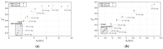
Figure 3.
Tvis vs. sheet resistance for varying silver thicknesses in the AZO (10 nm)/Ag/AZO (10 nm) structure: (a) using 200 W; (b) using 500 W.
Among the samples within the same series, the deposition conditions remain constant, and only the thickness of the deposited silver varies. At 200 W, the results at both flow rates are very similar, while, for 500 W, the samples at 1000 sccm show a higher transmittance, compared to those deposited at 300 sccm flow rates and the same power. Focusing on the range in which approximating to a linear trend is acceptable, the results are presented in Figure 4. Through applying these linear adjustments for each deposition condition, it is possible to eliminate the impact of depositing varying silver thickness. This allows us to compare samples that do not share the same Tvis or Rs values.
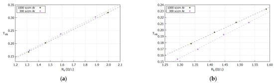
Figure 4.
Tvis vs. sheet resistance for varying silver thicknesses (data marked as “linear approximation” in Figure 3): (a) using 200 W; (b) using 500 W. The dashed line represents the linear fit when varying the silver thickness under each deposition condition.
Through visualization of these results, along with those previously obtained, a more comprehensive analysis can be achieved.
In this way, we can observe that, in the series in which the argon flow varies (Figure 5), when the sample at 1000 sccm is displaced parallel to the obtained trend, it remains higher than the other samples. This indicates that, via the adjustment of the silver thickness of the sample at 1000 sccm to achieve the same sheet resistance as the sample it is being compared to, a higher transmittance would be obtained than that of the reference sample.
Given this result, it has been deemed interesting to reexamine the effects of the power using the identified optimal flow rate of 1000 sccm. Both series with varying power are shown in Figure 6.
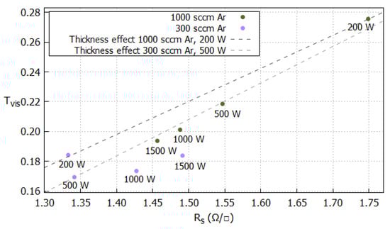
Figure 6.
The 300 and 1000 sccm argon flow (fixed). Visible transmittance factor against sheet resistance.
Regarding the series with variable power (Figure 6), the samples at 200 W are the only ones that remain above the trends. This aligns with the previous hypothesis, indicating that this is the optimal deposition condition. Furthermore, this hypothesis can be generalized, rather than only being valid for a specific flow rate.
These results differ from those obtained in [23]. Nevertheless, we consider them reliable because they were obtained under different conditions. The aforementioned article suggests that higher powers result in increased reflection in the mid-infrared range. However, this effect may be attributed to the increased thickness of the deposited silver, rather than to more favorable deposition conditions.
The observed dependence of properties on the deposited silver thickness aligns with the findings in [32]. As expected, greater thicknesses lead to a reduced transmittance and an increased reflectance. However, discounting the effect of the thickness, it is evident that silver layers deposited at a low power exhibit a higher visible transmittance.
3.4. Realistic Conditions
In this subsection, we analyze the results obtained for samples resembling those commercialized in the industry. These samples were deposited on glass, and the thickness of the AZO layers was increased to 47 nm. As a result, the high-transmission zone shifted toward longer wavelengths, as shown in Figure 7. Consequently, the resulting spectrum is more centered in the visible range, which is the desired outcome in low-emissivity coatings.
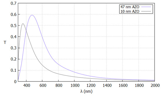
Figure 7.
Comparison of AZO (10 nm)/Ag (24 nm)/AZO (10 nm) vs. AZO (47 nm)/Ag (24 nm)/AZO (47 nm). Silver deposited at 200 W and 300 sccm.
The spectra corresponding to these samples can be visualized in Figure 8a. Once again, the difference is relatively small, but the sample at 200 W is consistently higher than the rest. Figure 8b shows the visible transmittance factor plotted against the sheet resistance. The sample at 200 W exhibits a higher transmittance, while the 500 W sample has lower Rs and, consequently, a lower emissivity.
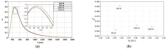
Figure 8.
Silver deposited at 300 sccm and different power levels with the AZO (47 nm)/Ag (24 nm)/AZO (47 nm): (a) transmittance spectrum in the visible and near-infrared range; (b) visible transmittance factor against sheet resistance.
For these samples, which are designed to resemble low-emissivity coatings, reflection spectra in the mid-infrared range were obtained, Figure 9. All samples exhibited an emissivity of approximately 97%, with only minor differences observed among them. Notably, the samples deposited at 200 and 500 W showed the highest reflectance, which is consistent with our previous findings.
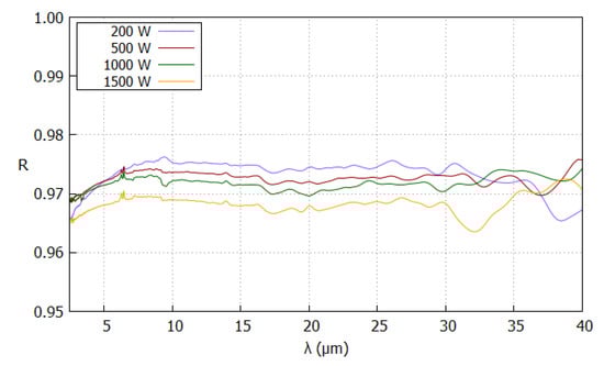
Figure 9.
The reflectance spectra in the mid-infrared range, series at 300 sccm, and different power levels, with 47 nm AZO.
Both the methods used to calculate the emissivity were compared, and the results are presented in Table 2. Clearly, the obtained values differ. This discrepancy is believed to be attributed to various sources of error in the reflection measurement with the spectrophotometer, such as sample inhomogeneity, pattern variability, and the concentration of CO2 and water in the atmosphere (which affect the absorption spectra), among others. On the other hand, sheet resistance measurements exhibit a higher consistency and fewer random errors. Thus, they have been used for the comparison.
Table 2.
Comparison of the methods used to calculate the emissivity. ϵn is the emissivity obtained from the IR reflectance spectrum using Equation (2), while ϵ is the emissivity obtained from Rs using Equation (3).
4. Conclusions
The aim of this study was to investigate the optimal conditions for silver deposition in low-emissive thin-film coatings. We explored how the samples varied when keeping all parameters constant, while modifying only the flow or power (with the appropriate carrier speed adjustment). We studied the effects of the thickness, both within a narrow range and an extended range, and considered these in our analysis. We also deposited samples with more realistic parameters. Furthermore, we compared the emissivity obtained using different methods.
Based on the results obtained in this study, it can be concluded that the optimal deposition conditions for silver in the fabrication of low-emissivity coatings, using a deposition system with similar dimensions to the one used in this study, correspond to a power of 200 W and an argon flow of 1000 sccm. To achieve the same results using another system, it is crucial to ensure that the target dimensions match. More generally, this can be extrapolated to 3.33 W/cm2. These conditions allow for samples with a higher transmittance in the visible light range and, at the same time, a lower sheet resistance and, thus, a lower emissivity.
The main drawback of depositing at 200 W is a longer deposition time. As demonstrated, the carrier speed is almost proportional to the supplied power, which means that achieving the same thickness takes more than twice the time at 200 W compared to at 500 W.
It has also been observed that less-optimal conditions are obtained with the powers of 1000 and 1500 W, as they generally produce samples with a higher sheet resistance. This has a negative impact on the optical and emissive properties of the coatings, limiting their energy efficiency and heat transfer reduction capabilities.
The results obtained in this study offer valuable insights into the fabrication of highly efficient and optically superior low-emissivity coatings. The identified optimal conditions correspond to low power settings and higher argon flow rates, providing important guidelines for practical applications in the industry.
Supplementary Materials
The following supporting information can be downloaded at: https://www.mdpi.com/article/10.3390/coatings13091556/s1, Figure S1: Transmittance spectrum of the AZO (10 nm)/Ag/AZO (10 nm) multilayer for different silver layer thicknesses deposited at 200 W and 300 sccm: between 300 and 2000 nm (top) and between 300 and 800 nm (bottom).
Author Contributions
Conceptualization, E.C.; methodology, C.C., N.H. and E.C.; formal analysis, C.C. and N.H.; investigation, C.C.; data curation, C.C.; writing—original draft preparation, C.C. and E.C.; writing—review and editing, C.C., N.H. and E.C.; visualization, C.C.; supervision, E.C.; project administration, E.C.; funding acquisition, E.C. All authors have read and agreed to the published version of the manuscript.
Funding
This research was funded by GOBIERNO DE ARAGON, grant number T20_20R.
Institutional Review Board Statement
Not applicable.
Informed Consent Statement
Not applicable.
Data Availability Statement
Not applicable.
Acknowledgments
We gratefully acknowledge the financial support of the “Departamento de Ciencia, Universidad y Sociedad del Conocimiento del Gobierno de Aragón” (group T20_20R).
Conflicts of Interest
The authors declare no conflict of interest.
References
- Schaefer, C.; Bräuer, G.; Szczyrbowski, J. Low Emissivity Coatings on Architectural Glass. Surf. Coat. Technol. 1997, 93, 37–45. [Google Scholar] [CrossRef]
- Martín-Palma, R.J.; Vázquez, L.; Martínez-Duart, J.M.; Riera, M. Silver-Based Low-Emissivity Coatings for Architectural Windows: Optical and Structural Properties. Sol. Energy Mater. Sol. Cells 1998, 53, 55–66. [Google Scholar] [CrossRef]
- Ding, G.; Clavero, C. Silver-Based Low-Emissivity Coating Technology for Energy-Saving Window Applications; IntechOpen: London, UK, 2017; ISBN 978-953-51-3004-8. [Google Scholar]
- Rabizadeh, M.; Ehsani, M.H.; Shahidi, M.M. ZnO/Metal/ZnO (Metal = Ag, Pt, Au) Films for Energy-Saving in Windows Application. Sci. Rep. 2022, 12, 15575. [Google Scholar] [CrossRef]
- Sun, K.; Zhang, D.; Yin, H.; Cheng, L.; Yuan, H.; Yang, C. Preparation of AZO/Cu/AZO Films with Low Infrared Emissivity, High Conductivity and High Transmittance by Adjusting the AZO Layer. Appl. Surf. Sci. 2022, 578, 152051. [Google Scholar] [CrossRef]
- Zhang, D.; Sun, K.; Yin, H.; Cheng, L.; Yuan, H.; Yang, C. Optimization of Photoelectric Properties and Temporal Stability of AZO/Ti/Cu/AZO Films by Insertion of Ti Layer for Low Emissivity Applications. Mater. Sci. Eng. B 2023, 293, 116471. [Google Scholar] [CrossRef]
- Jiang, Y.; Pillai, S.; Green, M.A. Realistic Silver Optical Constants for Plasmonics. Sci. Rep. 2016, 6, 30605. [Google Scholar] [CrossRef]
- Vanegas Parra, H.S.; Calderón Velasco, S.; Alfonso Orjuela, J.E.; Olaya Florez, J.J.; Carvalho, S. Influence of Ag Doping on the Microstructural, Optical, and Electrical Properties of ZrSiN Coatings Deposited through Pulsed-DC Reactive Magnetron Sputtering. Coatings 2023, 13, 1154. [Google Scholar] [CrossRef]
- Ando, E.; Miyazaki, M. Durability of Doped Zinc Oxide/Silver/Doped Zinc Oxide Low Emissivity Coatings in Humid Environment. Thin Solid Films 2008, 516, 4574–4577. [Google Scholar] [CrossRef]
- Ando, E.; Suzuki, S.; Aomine, N.; Miyazaki, M.; Tada, M. Sputtered Silver-Based Low-Emissivity Coatings with High Moisture Durability. Vacuum 2000, 59, 792–799. [Google Scholar] [CrossRef]
- Jobst, P.J.; Stenzel, O.; Schürmann, M.; Modsching, N.; Yulin, S.; Wilbrandt, S.; Gäbler, D.; Kaiser, N.; Tünnermann, A. Optical Properties of Unprotected and Protected Sputtered Silver Films: Surface Morphology vs. UV/VIS Reflectance. Adv. Opt. Technol. 2014, 3, 91–102. [Google Scholar] [CrossRef]
- Depla, D. Chemical Stability of Sputter Deposited Silver Thin Films. Coatings 2022, 12, 1915. [Google Scholar] [CrossRef]
- Tran, T.; Shrestha, M.; Baule, N.; Wang, K.; Fan, Q.H. Stable Ultra-Thin Silver Films Grown by Soft Ion Beam-Enhanced Sputtering with an Aluminum Cap Layer. ACS Appl. Mater. Interfaces 2023, 15, 29102–29109. [Google Scholar] [CrossRef]
- Baygi, S.J.M. Effect of the Thin Silver Layer in SnO2/Ag/SnO2 Nano-Coatings with Low Emission for Energy Storage. J. Electron. Mater. 2023, 52, 4532–4539. [Google Scholar] [CrossRef]
- Carretero, E.; Cueva, A.; Preciado-Garbayo, J.; Sevillano, P. Improved Photoenergy Properties of Low-Emissivity Coatings Deposited by Sputtering with an Ion Gun Treatment. Vacuum 2022, 205, 111485. [Google Scholar] [CrossRef]
- Szczyrbowski, J.; Brauer, G.; Ruske, M.; Schilling, H.; Zmelty, A. New Low Emissivity Coating Based on TwinMag (R) Sputtered TiO2 and Si3N4 Layers. Thin Solid Films 1999, 351, 254–259. [Google Scholar] [CrossRef]
- Kulczyk-Malecka, J.; Kelly, P.J.; West, G.; Clarke, G.C.B.; Ridealgh, J.A.; Almtoft, K.P.; Greer, A.L.; Barber, Z.H. Investigation of Silver Diffusion in TiO2/Ag/TiO2 Coatings. Acta Mater. 2014, 66, 396–404. [Google Scholar] [CrossRef]
- Ferrara, M.; Castaldo, A.; Esposito, S.; D’Angelo, A.; Guglielmo, A.; Antonaia, A. AlN-Ag Based Low-Emission Sputtered Coatings for High Visible Transmittance Window. Surf. Coat. Technol. 2016, 295, 2–7. [Google Scholar] [CrossRef]
- Addonizio, M.L.; Ferrara, M.; Castaldo, A.; Antonaia, A. Air-Stable Low-Emissive AlN-Ag Based Coatings for Energy-Efficient Retrofitting of Existing Windows. Energy Build. 2021, 250, 111259. [Google Scholar] [CrossRef]
- Liu, S.-N.; Zhou, Y.-W.; Sha, T.-Y.; Wu, F.-Y. Fabrication and Characterization of the AZO/Ag/AZO Transparent Conductive Films Prepared by RF Magnetron Sputtering Using Powder Targets. Nanosci. Nanotechnol. Lett. 2015, 7, 743–748. [Google Scholar] [CrossRef]
- Chiba, K.; Kageyama, T.; Iwata, T.; Fujimori, N.; Oda, H. Fabrication and Optical Properties of Low-Emissivity Coatings of Indium Tin Oxide or AlSiN and Ag-Alloy Multilayer Films on Glass. Jpn. J. Appl. Phys. 2005, 44, 2070. [Google Scholar] [CrossRef]
- Vo, T.T.B.; Choi, D. Zinc Oxide and Indium Tin Oxide as Embedding Layers for Ultrathin-Silver-Based Transparent Electrodes: A Comparative Study. Thin Solid Films 2023, 777, 139909. [Google Scholar] [CrossRef]
- Cinali, M.B.; Coskun, O.D. Optimization of Physical Properties of Sputtered Silver Films by Change of Deposition Power for Low Emissivity Applications. J. Alloys Compd. 2021, 853, 157073. [Google Scholar] [CrossRef]
- Bocchese, F.; Brown, I.; Cornil, D.; Moskovkin, P.; Muller, J.; Kenny, S.D.; Smith, R.; Lucas, S. Low-E Glass Improvement by the Understanding and Control of the Ag Growth. Appl. Surf. Sci. 2023, 611, 155600. [Google Scholar] [CrossRef]
- Hernández, A.R.C.; Ontiveros, R.I.R.; Ponce, H.E.E.; Ramírez, J.M.O.; Michel, J.R.P.; Moller, J.A.D. Effect of Silver on Structural, Optical, and Electrical Properties of ZnO:Al/Ag/ZnO:Al Thin Films. Nova Sci. 2022, 14, 1–11. [Google Scholar] [CrossRef]
- Miao, D.; Jiang, S.; Shang, S.; Chen, Z. Highly Transparent and Infrared Reflective AZO/Ag/AZO Multilayer Film Prepared on PET Substrate by RF Magnetron Sputtering. Vacuum 2014, 106, 1–4. [Google Scholar] [CrossRef]
- Miao, D.; Jiang, S.; Shang, S.; Chen, Z. Infrared Reflective Properties of AZO/Ag/AZO Trilayers Prepared by RF Magnetron Sputtering. Ceram. Int. 2014, 40, 12847–12853. [Google Scholar] [CrossRef]
- Filip, A.V.; Sava, B.A.; Medianu, R.V.; Boroica, L.; Dinca, M.C.; Pascu, R.; Tigau, N.; Andrei, A.; Moldovan, A.; Dumitru, M.; et al. Ultrathin Films of Silver by Magnetron Sputtering. Inorganics 2022, 10, 235. [Google Scholar] [CrossRef]
- Vitelaru, C.; Parau, A.C.; Dinu, M.; Pana, I.; Constantin, L.R.; Sobetkii, A.; Iordache, I. Transparent Silver Coatings with Copper Addition for Improved Conductivity by Combined DCMS and HiPIMS Process. Metals 2022, 12, 1264. [Google Scholar] [CrossRef]
- Rizzo, A.; Tagliente, M.A.; Alvisi, M.; Scaglione, S. Structural and Optical Properties of Silver Thin Films Deposited by RF Magnetron Sputtering. Thin Solid Films 2001, 396, 29–35. [Google Scholar] [CrossRef]
- Mashaiekhy, J.; Shafieizadeh, Z.; Nahidi, H. Effect of Substrate Temperature and Film Thickness on the Characteristics of Silver Thin Films Deposited by DC Magnetron Sputtering. Eur. Phys. J. Appl. Phys. 2012, 60, 20301. [Google Scholar] [CrossRef]
- Sun, X.; Hong, R.; Hou, H.; Fan, Z.; Shao, J. Optical Properties and Structures of Silver Thin Films Deposited by Magnetron Sputtering with Different Thicknesses. Chin. Opt. Lett. 2006, 4, 366–369. [Google Scholar]
- EN 410:2011; Glass in Building—Determination of Luminous and Solar Characteristics of Glazing. European Standard, European Committee for Standardization: Brussels, Belgium, 2011.
- Technical Resources|CIE. Available online: https://cie.co.at/technical-work/technical-resources (accessed on 14 August 2023).
- EN 12898:2019; Glass in Building—Determination of the Emissivity. European Standard, European Committee for Standardization: Brussels, Belgium, 2019.
Disclaimer/Publisher’s Note: The statements, opinions and data contained in all publications are solely those of the individual author(s) and contributor(s) and not of MDPI and/or the editor(s). MDPI and/or the editor(s) disclaim responsibility for any injury to people or property resulting from any ideas, methods, instructions or products referred to in the content. |
© 2023 by the authors. Licensee MDPI, Basel, Switzerland. This article is an open access article distributed under the terms and conditions of the Creative Commons Attribution (CC BY) license (https://creativecommons.org/licenses/by/4.0/).