Abstract
Cadmium (Cd)-free photodiodes based on n-type Zinc Selenide/p-type Zinc Telluride (n-ZnSe/p-ZnTe) heterojunctions were prepared by Radio Frequency-Magnetron Sputtering (RF-MS) technique, and their detailed optical and electrical characterization was performed. Onto an optical glass substrate, 100 nm gold (Au) thin film was deposited by Thermal Vacuum Evaporation (TVE) representing the back-contact, followed by the successive RF-MS deposition of ZnTe, ZnSe, Zinc Oxide (ZnO) and Indium Tin Oxide (ITO) thin films, finally resulting in the Au/ZnTe/ZnSe/ZnO/ITO sub-micrometric “substrate”-type configuration. Next, the optical characterization by Ultraviolet-Visible (UV-VIS) spectroscopy was performed on the component thin films, and their optical band gap values were determined. The electrical measurements in the dark and under illumination at different light intensities were subsequently performed. The Current–Voltage (I–V) characteristics in the dark are nonlinear with a relatively high asymmetry, following the modified Shockley–Read equation. From their analysis, the series resistance, shunt resistance, the ideality factor and saturation current were determined with high accuracy. It is worth noting that the action spectrum of the structure is shifted to short wavelengths. A sensibility test for the 420–500 nm range was performed while changing the intensity of the incident light from 100 mW/cm down to 10 mW/cm and measuring the photocurrent. The obtained results provided sufficient information to consider the present sub-micrometric photodiodes based on n-ZnSe/p-ZnTe heterojunctions to be more suitable for the UV domain, demonstrating their potential for integration within UV photodetectors relying on environmentally-friendly materials.
1. Introduction
Zinc Telluride (ZnTe) and Zinc Selenide (ZnSe) are AII-BVI semiconducting compounds having good optical and electrical properties. With a wide and direct band gap varying from 2.67 eV up to 2.75 eV at room temperature for ZnSe, and 1.7 eV up to 2.26 eV for ZnTe [1,2,3], they are more sensitive to blue–green and ultraviolet (UV) light. Therefore, ZnSe having a low absorption coefficient in the visible range of solar spectrum and an appropriate refractive index is commonly used within optoelectronic devices such as blue-green laser diodes [4], white light and green light emitting diodes (LEDs) [4,5,6], in single–junctions as buffer material [2,7,8] or “window” layer [9,10], but also in multi–junction solar cells [2,11], as well as within photo-electro-chemical devices [12] or photodetectos [13]. In contrast, ZnTe presents a high optical absorption coefficient as well as high mobility [14], and its conduction profile can be easily changed by doping [15], thus making it suitable to be integrated into optoelectronic devices such as LEDs [16] and in particular blue [17] or green [18] emitting diodes, photovoltaic and new generation graded band gap solar cells [19,20], devices relying onto ZnTe/CdTe heterojunctions [21], thin film transistors, photodetectors [22,23], and electro-optic field detectors [17].
Since Rajakarunanayake et al. [24], studying these materials was considered to offer great promise when integrating them into devices for short wavelength semiconductor optoelectronics. In particular, ZnTe presents great potential as an inter-layer within Cadmium Telluride (CdTe)-based solar cells, forming a low resistance ohmic contact due to a small valence band offset (0.1 eV) between ZnTe and CdTe [25,26,27,28]. On these premises, Cadmium (Cd)-free ZnTe-based heterojunctions attracted much interest, mostly due to the negative impact Cd has upon the environment, and studies of morpho–structural and electrical properties of various more environmentally-friendly ZnTe-based heterojunctions are still a hot topic. Gupta et al. [29] mentioned that ZnSe/ZnTe heterojunctions present high valence band offset, confirmed also by other authors who computed this offset, finding the value of 1 eV, results suggesting that the ZnSe/ZnTe heterojunctions present good rectifying properties [30]. This type of heterojunction can contribute to reducing the harmful effect of Cd, by replacing some of the devices based on CdS/CdTe heterojunctions without significant performance losses [30,31].
Although a great amount of work was already devoted to studying the physical properties of both ZnSe and ZnTe sputtered thin films [1,27,32,33], little has been reported regarding the electrical characterization of ZnSe/ZnTe heterojunctions. Moreover, the present study attempts the fabrication of a “substrate”-type sub-micrometric multi-layered structure based on thin film n-ZnSe/p-ZnTe heterojunctions, focusing on the analysis of its optical and photoelectrical properties. Hence, the investigated architecture could represent a Cd-free environmentally-“green” device when comparing to other photodiode counterparts based on CdSe, CdS or CdTe materials, as well as being very thin, light-weight and low-cost.
2. Experimental Procedures
A Cd-free “substrate”-type structure based on a ZnSe/ZnTe heterojunction was obtained by evaporating onto a cost-effective optical borosilicate glass (N-BK7, Heinz Herenz Hamburg, Germany) 100 nm gold (Au) via Thermal Vacuum Evaporation (TVE) technique at Torr working pressure, maintaining through the entire deposition process a substrate temperature of 100 °C. This Au thin film represented the back-contact of the structure, providing an excellent ohmic conduction of the Au/ZnTe interface. ZnTe was then sputtered via Radio Frequency-Magnetron Sputtering (RF-MS). The deposition parameters were: 13.56 MHz (frecquency of the RF generator), 50 W RF working power and a mbar working pressure of the argon (Ar) gas. During this 60 min process, the substrate’s temperature was kept constant at 200 °C. The ZnTe thin film was followed by ZnSe sputtered at 100 W RF power, mbar working pressure and 220 °C substrate’s temperature for 20 min. Afterwards, a zinc oxide (ZnO) ultra-thin film was sputtered onto Au/ZnTe/ZnSe at 50 W RF power, while the working pressure during this deposition carried out at room temperature was mbar, and the duration of the process was 35 min. Finally, an indium tin oxide (ITO) thin film was also deposited by RF-MS at 80 W and mbar for 40 min at room temperature. This latter thin film completed the Au/ZnTe/ZnSe/ZnO/ITO sub-micrometric structure. During all sputtering procedures, the target-to-substrate distance was kept constant at 9 cm. The obtained Au/ZnTe/ZnSe/ZnO/ITO structure is schematically represented in Figure 1a, as well as in the top- and back-side view photographs shown in Figure 1b. It is worth noting that the effective device area formed by successively overlapping the films was about 0.2 cm, much smaller than the substrate’s surface, in order to avoid potentially occurring edge effects such as short-circuits between the layers.
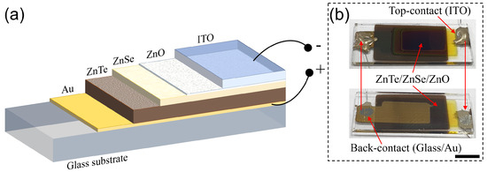
Figure 1.
(a) Schematic representation of the Au/ZnTe/ZnSe/ZnO/ITO sub-micrometric structure prepared onto an optical glass substrate; (b) corresponding top- and back-side CCD images of the prepared structure. The scale bar is 5 mm.
More details are presented in our previous papers focused on the morpho-structural characterizations of ZnSe [1,32], ZnTe [27,33] and ZnO [34,35], respectively. Herewith, the thickness of the ZnO ultra-thin film was first evaluated by means of X-ray reflectometry (XRR) using a Bruker D8 Discover Diffractometer (Bruker, Billerica, MA, USA) operating with CuK radiation ( nm). Optical properties of ITO, ZnSe and ZnTe thin films were subsequently investigated by transmission and optical absorption measurements in the 300–1500 nm spectral range at room temperature by using an UV-VIS PerkinElmer Lambda 750 spectrophotometer (PerkinElmer, Waltham, MA, USA). Via optical transmission spectra, the thickness values of ITO, ZnSe and ZnTe were evaluated, whereas their optical band gap energy was computed from the optical absorption spectra. Both current–voltage (I–V) characteristics in the dark and action spectrum at AM 1.5 illumination conditions of the Au/ZnTe/ZnSe/ZnO/ITO structure were measured at room temperature. The corresponding transport mechanism and electrical parameters of the structure were identified. Moreover, a sensibility test, as a UV detector, of the structure for the 420–500 nm range of solar spectrum was performed by varying the incident wavelength’s intensity from 100 mW/cm down to 10 mW/cm and measuring the photocurrent electrical intensity.
3. Results and Discussion
3.1. Structural Characterization
The structural properties of the ZnSe and ZnTe thin films, obtained in the same conditions, were presented in detail in our previous papers, i.e., [1,32] for ZnSe and [27,33] for ZnTe thin films, respectively. Additional studies have shown a weak tendency to a crystallographic texture and preferential orientation of sputtered ZnO ultra-thin films, attributed to the reduced plasma power and associated low sputtering rate [34,35]. Indeed, the thickness of the ZnO film was evaluated by XRR at roughly 55 nm, as resulting from the spectrum presented in Figure 2. The latter method uses total external reflection from surfaces being suitable for estimating layer thicknesses in this range of values, where the positions of interference fringes within reflectivity curve can be used to determine the film thickness by the modified Bragg equation [36]:
where is the ZnO thickness, is the observed position of the ith interference fringe (expressed in radians), is the critical angle for total reflection expressed in radians (see Figure 2), m is the integer number of fringe, and is the wavelength of the incident X-ray.

Figure 2.
X-ray reflectometry (XRR) spectrum that allowed thickness evaluation of the ultra-thin ZnO film as ∼55 nm.
3.2. Optical Characterization
Transmission spectra of the ITO, ZnO, ZnSe and ZnTe sputtered onto glass substrates (the same deposition parameters) are emphasized in Figure 3a. As can be noticed, both ITO and ZnO are transparent over almost all the entire spectral region, enough to allow light to reach the “window” layer interface without any considerable losses. As far as the ZnSe and ZnTe spectra are concerned, one may easily see the high transmittance in the infra-red region that both thin films have, with values larger than 70%. Transmission spectra were further used to compute the films’ thicknesses by using the “two-envelopes” method [37]. The latter implies constructing the two envelope functions around the minima and maxima of the interference fringes within transparent region. Plotting the linear dependence of as function of obeying Equation (2) for ITO, ZnSe and ZnTe allowed the evaluation of the slope as twice the film’s thickness (see Figure 3b–d):
where is related to the minimum and maximum interference conditions, n is the commonly reported refractive index corresponding to each material (1.83 for ITO [38], 2.67 for ZnSe [39] and 3.56 for ZnTe [40]), is the associated wavelength of the minimum or maximum point, d is the film’s thickness, whereas represents the order of the first interference fringe [41,42]. In this way, the transmission spectra of ITO, ZnSe and ZnTe permitted the evaluation of their corresponding thicknesses as about: nm for ITO (see Figure 3b), nm for ZnSe (see Figure 3c) and nm for ZnTe (see Figure 3d), whereas the indicated uncertainties represent the standard error of the linear regressions.
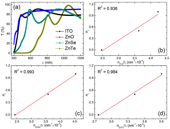
Figure 3.
(a) Optical transmission spectra of the ITO, ZnO, ZnSe and ZnTe thin films, RF-sputtered onto optical glass substrates; (b–d) corresponding plots used for thickness evaluation of ITO (b), ZnSe (c) and ZnTe (d), respectively, as twice the slope of linear dependency. denotes the coefficient of determination for the fit of the linear regressions.
The thickness values obtained from the transmission spectra for ITO, ZnSe and ZnTe were used to compute the optical band gap energies of the fabricated thin films by employing the absorption spectra presented in Figure 4 and Tauc’s plot method (see the insets of Figure 4a–c). In order to compute the values for band gap energy of ITO, ZnSe and ZnTe, the dependence of absorption coefficient () on the energies of incident photons () must be performed. By using relation (3), we can obtain as the ratio between the optical absorbance of the thin film (A) and its thickness (d):

Figure 4.
Absorbance spectra of the RF-sputtered ITO (a), ZnSe (b) and ZnTe (c), representing the dependency of the optical absorbance coefficient on the incident photons. The insets represent corresponding linear fit representation (using Tauc’s method) utilized to compute the optical band gap energies of the thin films.
Subsequently, the dependence of absorption coefficient on the incident photon energies for direct band gap semiconductors (such as cubic phase ZnSe and ZnTe) near the fundamental absorption edge is described by the following equation [43,44]:
where is the photon energy, and is the optical band gap corresponding to the Γ point of the first Brillouin zone. Thus, fitting the experimental data with Equation (4), optical band gap energies of ZnSe and ZnTe films, respectively, were obtained. The calculated values for the band gap energies of the sputtered films are 3.54 eV for ITO (see Figure 4a), 2.73 eV for the ZnSe (see Figure 4b) and 2.08 eV for the ZnTe (see Figure 4c), values that are in good agreement with the theoretical and other experimental determinations [1,2,3,33,45].
3.3. Electrical and Photoelectrical Measurements
The electrical measurements in the dark of this heterojunction revealed a nonlinear I–V characteristics with relatively high asymmetry (see Figure 5a), the rectifying factor being estimated to be around 50 at 1.25 V. Taking into account the optical band gap energy values of both materials determined herewith (see Figure 4) as well as in our previous papers (i.e., [1,32] for ZnSe and [27,33] for ZnTe, respectively), a theoretical energy band diagram for n-ZnSe/p-ZnTe heterojunction, constructed on the basis of Anderson’s model, would be similar to the one reported by Rao et al. [30,46] with particularly replacing in the latter the energy parameters of CdS with the ones of ZnSe. In this context, the observed asymmetry of the dark I–V characteristics is due to the heterojunction present at the ZnSe/ZnTe interface, the Au back-electrode and the ZnO/ITO top-electrode featuring a good ohmic behaviour. Analysing further the measured I–V characteristics in the dark, we found that it follows the modified Shockley–Read equation [47,48,49,50]:
where I is the current flowing just through the heterojunction, is the saturation current, q is the elementary charge, U is the applied voltage to the whole structure, n is the ideality factor of the diode, is the Boltzmann constant, and and are the series and shunt resistances, respectively. By performing the logarithmic plot of the intensity of the current, i.e., Equation (5) at forward bias, as a function of the applied voltage, i.e., versus U (see Figure 5b), a first determination of the diode ideality factor is obtained () along with the saturation current ( A) [26,49,50]. Both values are not accurately computed due to the great impact of series and shunt resistances, i.e., and , on the linearity of this plot. Therefore, the second step was to remove the effect of the series resistance and shunt resistance on this procedure to accurately evaluate the ideality factor and saturation current. To find these resistances, the differential resistance of the structure () is plotted versus the reciprocal current, i.e., , as the Equation (6) suggests [26,47,48,49,50,51]:
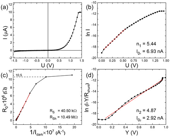
Figure 5.
(a) Current –voltage (I–V) dark ambipolar characteristics recorded at room temperature of the Au/ZnTe/ZnSe/ZnO/ITO “sandwich” structure; (b) semi-logarithmic fit ( vs. U) at forward bias, allowing the determination of ideality factor and saturation current; (c) dependency of as a function of reciprocal dark current permitting the evaluation of series and shunt resistances; (d) linear representation, i.e., vs. Y, illustrating the more accurate determination of the ideality factor and saturation current.
The computed values are 40.5 kΩ and 10.5 MΩ for the series and shunt resistances, respectively (see Figure 5c). The final step, in order to obtain more accurate values for the ideality factor and saturation current, are a change in variable for the voltage (U) applied to the structure to the drop voltage (Y) across the heterojunction, i.e., , and a subsequent semi-logarithmic plot of real current crossing the heterojunction, as a function of Y, see Figure 5d that obeys the modified Shockley–Read equation [50,51]:
where . One can easily see that, after eliminating the effect of both series and shunt resistances, the linearity in the plot from Figure 5d was extended allowing the evaluation of the ideality factor and saturation current with better accuracy, as: and A, respectively. The relatively high value obtained for the diode’s ideality factor, but comparable with other similar structures (i.e., in [52]), is typically expected in thin film-based devices due to the fine grain structure of the films. Unlike the high-end techniques such as molecular beam epitaxy (MBE), the RF-MS films have much less grain size and large grain boundary regions containing a lot of defects limiting the flow of the free charges by acting as carrier traps, as also shown in one of our recent papers [27].
Figure 6a displays the action spectrum (external quantum efficiency—EQE) of the Au/ZnTe/ZnSe/ZnO/ITO structure when illuminating it at AM 1.5 conditions. This EQE illustrates that the photo-generation process takes place, as expected, at small wavelengths, taking into account the threshold wavelengths for ZnSe and ZnTe ( nm and nm). According to Figure 6a, a large peak is observed around 450 nm, which corresponds to the photon energy of about 2.7 eV, resulting from the photon absorption within ZnSe layer. A second very small peak is also visible around 550 nm, corresponding to the energy band gap of ZnTe (i.e., ∼2.1 eV). One may thus easily notice that the action spectrum is strongly shifted to the UV domain—the barrier at ZnSe/ZnTe interface is shifted to the ZnO/ZnSe interface (thus the obtained maximum at 450 nm corresponds to ZnSe’s threshold wavelength). The observed behaviour is expected, while observing the good agreement of the obtained optical band gap values of ZnSe and ZnTe, respectively, with equation:
where is the optical band gap expressed in eV, is the product between Plank’s constant and speed of light in vacuum (i.e., 1.23985) and is the wavelength expressed in μm. In our structure, light first falls onto the n-type ZnSe layer where only wavelengths below 450 nm are absorbed, and the rest of the wavelengths are either reflected or transmitted towards the p-type ZnTe layer. The p-type layer only absorbs photons which have wavelengths below the one corresponding to its band gap, and, being very thin, its contribution to photogeneration is very low. Indeed, the I–V characteristics of the heterojunction under illumination in AM 1.5 conditions show a very low photocurrent and photo-voltage. This behavior was mentioned also by other authors concluding that, in the regime of photoelement, a power conversion efficiency of ∼10% can only be obtained for multi-junction solar cells containing CdTe [2] or CdSe [53] in conjunction with ZnSe and ZnTe thin films. Ultimately, observing that our structure behaves better in the regime of a photodiode, a light sensibility test for the 420–500 nm range was also performed by varying incident wavelength’s intensity from 100 mW/cm down to 10 mW/cm and measuring the photocurrent intensity (see Figure 6b). The variation of maximum sensitivity photocurrent () at 450 nm with the power of the incident light (P) is shown in Figure 6c. Theoretically, the photocurrent in a thin film photodiode varies with light power density according to the relation:
where k is a number which can be equal to, less than or greater than 1, corresponding to linear, sub-linear and super linear behaviors, respectively [52,54]. In the present study, the variation of with P was found to be slightly sub-linear (). The sub-linear variation in the ZnSe/ZnTe heterojunction results from the exponential distribution of carrier traps in the band gap of both polycrystalline thin films [27,54]. As intensity of the radiation increases, the quasi-Fermi level shifts towards the conduction band edge, increasing the number of traps that are converted into recombination centers; then, the photocurrent does not increase linearly with power density. All these observations clearly suggest that the present device is more suitable for UV-based sensor applications as UV photodetectors.
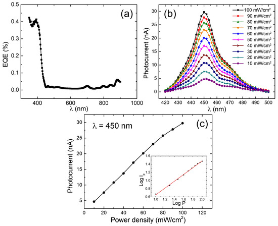
Figure 6.
(a) The action spectrum of the Au/ZnTe/ZnSe/ZnO/ITO “sandwich” structure at AM 1.5 illumination condition; (b) photo-sensibility test of the present structure between 100 mW/cm and 10 mW/cm incident wavelength intensity; (c) maximum sensitivity photocurrent (), taken at = 450 nm, represented as a function of the power of the incident light. The inset: corresponding log-log representation of the photocurrent versus power density with a sub-unitary slope of the linear regression ().
4. Conclusions
Cd-free photodiodes based on n-ZnSe/p-ZnTe heterojunction structures were prepared by the RF-MS technique. The optical characterization, via UV-VIS spectroscopy, illustrated that ITO and ZnO have high transparency (with values larger than 85%) as they should, given their common use as transparent conducting oxide (TCO) materials. The transmission spectra of ITO, ZnSe and ZnTe permitted the computation of their thicknesses as 275 nm, 237 nm and 437 nm, respectively. Using the Tauc’s plot method from the absorption spectra, the optical band gap energies of all three sputtered thin films were evaluated to 3.54 eV for ITO, 2.73 eV for ZnSe and 2.08 eV for ZnTe. Fitting the experimental data obtained from the dark I–V characteristics of the diodes recorded at room temperature, with modified Shockley–Read’s equation, the shunt and series resistances (10.49 MΩ and 40.5 kΩ, respectively) of the diodes were determined and a method to compute with high accuracy the ideality factor and the saturation current of the heterojunction was presented. Based on this model, a diode ideality factor of 4.87 and a saturation current value of 2.92 nA were obtained. The action spectrum at illumination in AM 1.5 conditions showed that a low photovoltaic response shifted in the UV range of the solar spectrum, as expected considering the values of the optical band gap of ZnTe and ZnSe. However, the photo-response in this range of wavelengths (420–500 nm) strongly changed when the light intensity changes from 100 mW/cm down to 10 mW/cm. The maximum sensitivity is at a wavelength of 450 nm. Based on these results, we have considered the present n-ZnSe/p-ZnTe heterojunction–based sub-micrometric structure to be more suitable for applications sensitive to the UV domain, thus with the potential to be integrated within sensitive UV photodetectors.
Author Contributions
Conceptualization, A.-M.P. and V.-A.A.; methodology, A.-M.P. and V.-A.A.; software, A.-M.P. and V.-A.A.; validation, V.-A.A.; formal analysis, A.-M.P.; investigation, A.-M.P.; resources, V.-A.A.; writing—original draft preparation, A.-M.P.; writing—review and editing, A.-M.P. and V.-A.A.; supervision, V.-A.A.; project administration, V.-A.A.; funding acquisition, V.-A.A. All authors have read and agreed to the published version of the manuscript.
Funding
This research was funded by the “Executive Unit for Financing Higher Education, Research, Development and Innovation” (UEFISCDI, Romania), through the grant: 115/2020 (PN-III-P1-1.1-TE-2019-0868).
Institutional Review Board Statement
Not applicable.
Informed Consent Statement
Not applicable.
Data Availability Statement
The data used and/or analyzed during the current study are available from the corresponding author on reasonable request.
Conflicts of Interest
The authors declare no conflict of interest. The funders had no role in the design of the study; in the collection, analyses, or interpretation of data; in the writing of the manuscript; or in the decision to publish the results.
Abbreviations
The following abbreviations are used in this manuscript:
| MDPI | Multidisciplinary Digital Publishing Institute |
| R&D | Research & development |
| MDEO | R&D Center for Materials and Electronic & Optoelectronic Devices |
| IMCN | Institute of Condensed Matter and Nanosciences |
| UCLouvain | Université Catholique de Louvain |
| LED | Light emitting diode |
| RF-MS | Radio frequency magnetron sputtering |
| TVE | Thermal Vacuum Evaporation |
| ITO | Indium Tin Oxide |
| TCO | Transparent conducting oxide |
| XRD | X-ray diffraction |
| XRR | X-ray reflectometry |
| VIS | Visible spectral region |
| UV | Ultraviolet spectral region |
| NIR | Near-infrared spectral region |
| EQE | External quantum efficiency |
| MBE | Molecular beam epitaxy |
| UEFISCDI | Executive Unit for Financing Higher Education, Research, Development and Innovation |
References
- Toma, O.; Antohe, V.A.; Panaitescu, A.M.; Iftimie, S.; Răduţă, A.M.; Radu, A.; Ion, L.; Antohe, Ş. Effect of RF Power on the Physical Properties of Sputtered ZnSe Nanostructured Thin Films for Photovoltaic Applications. Nanomaterials 2021, 11, 2841. [Google Scholar] [CrossRef] [PubMed]
- Saikia, P.; Saikia, P.K.; Saikia, D. Fabrication and characterization of ZnSe/ZnTe/CdTe/HgTe multijunction solar cell. Optoelectron. Adv. Mater. Rapid Commun. 2011, 5, 204–207. [Google Scholar]
- Rathod, K.C.; Sanadi, K.R.; Kamble, P.D.; Kamble, G.S.; Gaur, M.L.; Garadkar, K.M. Growth Mechanism, Structural and Photoelectrochemical Study of Zinc Tellurium Thin Film. Asian J. Chem. 2022, 34, 715–719. [Google Scholar] [CrossRef]
- Qian, L.; Zhang, T.; Teng, F.; Xu, Z.; Quan, S. Luminescent properties and excitation mechanism of ZnSe quantum dots embedded in ZnS Matrix. Mater. Chem. Phys. 2006, 100, 337–339. [Google Scholar] [CrossRef]
- Ou, K.; Wang, S.; Wan, G.; Huang, M.; Zhang, Y.; Bai, L.; Yi, L. A study of structural, morphological and optical properties of nanostructured ZnSe/ZnS multilayer thin films. J. Alloys Compd. 2017, 726, 707–711. [Google Scholar] [CrossRef]
- Mehta, C.; Saini, G.S.S.; Abbas, J.M.; Tripathi, S.K. Effect of deposition parameters on structural, optical and electrical properties of nanocrystalline ZnSe thin films. Appl. Surf. Sci. 2009, 256, 608–614. [Google Scholar] [CrossRef]
- Prabhu, M.; Kamalakkannan, K.; Soundararajan, N.; Ramachandran, K. Fabrication and characterization of ZnSe thin films based low-cost dye sensitized solar cells. J. Mater. Sci. Mater. Electron. 2015, 26, 3963–3969. [Google Scholar] [CrossRef]
- Eisele, W.; Ennaoui, A.; Schubert-Bischoff, P.; Giersig, M.; Pettenkofer, C.; Krauser, J.; Lux-Steiner, M.; Zweigart, S.; Karg, F. XPS, TEM and NRA investigations of Zn(Se,OH)/Zn(OH)2 films on Cu(In,Ga)(S,Se)2 substrates for highly efficient solar cells. Sol. Energy Mater. Sol. Cells 2003, 75, 17–26. [Google Scholar] [CrossRef]
- Subbaiah, Y.P.V.; Prathap, P.; Devika, M.; Reddy, K.T.R. Close-spaced evaporated ZnSe films: Preparation and characterization. Phys. B Condens. Matter 2005, 365, 240–246. [Google Scholar] [CrossRef]
- Antohe, Ş.; Ion, L.; Gîrtan, M.; Toma, O. Optical and morphological studies of thermally vacuum evaporated ZnSe thin films. Rom. Rep. Phys. 2013, 65, 805–811. [Google Scholar]
- Islam, A.B.M.O.; Chaure, N.B.; Wellings, J.; Tolan, G.; Dharmadasa, I.M. Development of electrodeposited ZnTe layers as window materials in ZnTe/CdTe/CdHgTe multi-layer solar cells. Mater. Charact. 2009, 60, 160–163. [Google Scholar] [CrossRef]
- Venkatachalam, S.; Mangalaraj, D.; Narayandass, S.K.; Kim, K.; Yi, J. Composition, structural, dielectric and DC characterization of vacuum deposited ZnSe thin films. Vacuum 2007, 81, 928–933. [Google Scholar] [CrossRef]
- Lin, T.K.; Chang, S.J.; Su, Y.K.; Chiou, Y.Z.; Wang, C.K.; Chang, S.P.; Chang, C.M.; Tang, J.J.; Huang, B.R. ZnSe MSM photodetectors prepared on GaAs and ZnSe substrates. Mater. Sci. Eng. B 2005, 119, 202–205. [Google Scholar] [CrossRef]
- Singh, H.; Singh, M.; Singh, J.; Bansod, B.S.; Singh, T.; Thakur, A.; Wani, M.F.; Sharma, J. Composition dependence study of thermally evaporated nanocrystalline ZnTe thin films. J. Mater. Sci. Mater. Electron. 2019, 30, 3504–3510. [Google Scholar] [CrossRef]
- Olusola, O.I.; Madugu, M.L.; Abdul-Manaf, N.A.; Dharmadasa, I.M. Growth and characterisation of n- and p-type ZnTe thin films for applications in electronic devices. Curr. Appl. Phys. 2016, 16, 120–130. [Google Scholar] [CrossRef]
- Hussain, T.; Al-Kuhaili, M.F.; Durrani, S.M.A.; Qayyum, H.A. Influence of angle deposition on the properties of ZnTe thin films prepared by thermal evaporation. Ceram. Int. 2018, 44, 10130–10140. [Google Scholar] [CrossRef]
- Kumar, V.; Kumar, V.; Dwivedi, D.K. Growth and characterization of zinc telluride thin films for photovoltaic applications. Phys. Scr. 2012, 86, 015604. [Google Scholar] [CrossRef]
- Sato, K.; Asahi, T.; Hanafusa, M.; Noda, A.; Arakawa, A.; Uchida, M.; Oda, O.; Yamada, Y.; Taguchi, T. Development of Pure Green LEDs Based on ZnTe. Phys. Status Solidi (a) 2000, 180, 267–274. [Google Scholar] [CrossRef]
- Toma, O.; Antohe, Ş. Optical and morphological investigations of thermally vacuum evaporated ZnTe thin films. Chalcogenide Lett. 2014, 11, 611–618. [Google Scholar]
- Fauzi, F.; Diso, D.G.; Echendu, O.K.; Patel, V.; Purandare, Y.; Burton, R.; Dharmadasa, I.M. Development of ZnTe layers using an electrochemical technique for applications in thin-film solar cells. Semicond. Sci. Technol. 2013, 28, 045005. [Google Scholar] [CrossRef]
- Toma, O.; Ion, L.; Gîrtan, M.; Antohe, Ş. Optical, morphological and electrical studies of thermally vacuum evaporated CdTe thin films for photovoltaic applications. Sol. Energy 2014, 108, 51–60. [Google Scholar] [CrossRef]
- Cao, Y.L.; Liu, Z.T.; Chen, L.M.; Tang, Y.B.; Luo, L.B.; Jie, J.S.; Zhang, W.J.; Lee, S.T.; Lee, C.S. Single-crystalline ZnTe nanowires for application as high-performance Green/Ultraviolet photodetector. Opt. Express 2011, 19, 6100–6108. [Google Scholar] [CrossRef] [PubMed]
- Singh, H.; Singh, P.; Thakur, A.; Singh, T.; Sharma, J. Nanocrystalline ZnxTe100-x (x = 0, 5, 20, 30, 40, 50) thin films: Structural, optical and electrical properties. Mater. Sci. Semicond. Process. 2018, 75, 276–282. [Google Scholar] [CrossRef]
- Rajakarunanayake, Y.; Miles, R.H.; Wu, G.Y.; McGill, T.C. Band offset of the ZnSe-ZnTe superlattices: A fit to photoluminescence data by k·p theory. J. Vac. Sci. Technol. B Microelectron. Process. Phenom. 1988, 6, 1354–1359. [Google Scholar] [CrossRef]
- Späth, B.; Fritsche, J.; Säuberlich, F.; Klein, A.; Jaegermann, W. Studies of sputtered ZnTe films as interlayer for the CdTe thin film solar cell. Thin Solid Film. 2005, 480–481, 204–207. [Google Scholar] [CrossRef]
- Ion, L.; Enculescu, I.; Iftimie, S.; Ghenescu, V.; Tăzlăoanu, C.; Beşleagă, C.; Mitran, T.L.; Antohe, V.A.; Gugiu, M.M.; Antohe, Ş. Effects of proton irradiation on the spectral performance of photovoltaic cells based on CdS/CdTe thin films. Chalcogenide Lett. 2010, 7, 521–530. [Google Scholar]
- Panaitescu, A.M.; Antohe, I.; Răduţă, A.M.; Iftimie, S.; Antohe, Ş.; Mihăilescu, C.N.; Antohe, V.A. Morphological, optical, and electrical properties of RF-sputtered zinc telluride thin films for electronic and optoelectronic applications. AIP Adv. 2022, 12, 115013. [Google Scholar] [CrossRef]
- Suthar, D.; Chuhadiya, S.; Sharma, R.; Himanshu; Dhaka, M.S. An overview on the role of ZnTe as an efficient interface in CdTe thin film solar cells: A review. Mater. Adv. 2022, 3, 8081–8107. [Google Scholar] [CrossRef]
- Gupta, M.C.; Ballato, J. (Eds.) The Handbook of Photonics, 2nd ed.; CRC Press: Boca Raton, FL, USA, 2006; 1040p, ISBN 9780849330957. [Google Scholar]
- Rao, G.K.; Bangera, K.V.; Shivakumar, G.K. Studies on vacuum deposited p-ZnTe/n-ZnSe heterojunction diodes. Solid-State Electron. 2010, 54, 787–790. [Google Scholar] [CrossRef]
- Chasta, G.; Himanshu; Patel, S.L.; Chander, S.; Kannan, M.D.; Dhaka, M.S. Analysis of different vacuum annealing levels for ZnSe thin films as potential buffer layer for solar cells. J. Mater. Sci. Mater. Electron. 2022, 33, 139–157. [Google Scholar] [CrossRef]
- Ion, L.; Iftimie, S.; Radu, A.; Antohe, V.A.; Toma, O.; Antohe, Ş. Physical properties of RF-sputtered ZnSe thin films for photovoltaic applications: Influence of film thickness. Proc. Rom. Acad. Ser. A 2021, 22, 25–34. [Google Scholar]
- Manica, D.; Antohe, V.A.; Moldovan, A.; Pascu, R.; Iftimie, S.; Ion, L.; Şuchea, M.P.; Antohe, Ş. Thickness Effect on Some Physical Properties of RF Sputtered ZnTe Thin Films for Potential Photovoltaic Applications. Nanomaterials 2021, 11, 2286. [Google Scholar] [CrossRef] [PubMed]
- Locovei, C.; Coman, D.; Radu, A.; Ion, L.; Antohe, V.A.; Vasile, N.; Dumitru, A.; Iftimie, S.; Antohe, Ş. Physical properties of Cu and Dy co-doped ZnO thin films prepared by radio frequency magnetron sputtering for hybrid organic/inorganic electronic devices. Thin Solid Film. 2019, 685, 379–384. [Google Scholar] [CrossRef]
- Beşleagă, C.; Stan, G.E.; Gâlcă, A.C.; Ion, L.; Antohe, Ş. Double layer structure of ZnO thin films deposited by RF-magnetron sputtering on glass substrate. Appl. Surf. Sci. 2012, 258, 8819–8824. [Google Scholar] [CrossRef]
- Huang, T.C.; Gilles, R.; Will, G. Thin-film thickness and density determination from X-ray reflectivity data using a conventional power diffractometer. Thin Solid Film. 1993, 230, 99–101. [Google Scholar] [CrossRef]
- Ur Rehman, K.M.; Liu, X.; Riaz, M.; Yang, Y.; Feng, S.; Khan, M.W.; Ahmad, A.; Shezad, M.; Wazir, Z.; Ali, Z.; et al. Fabrication and characterization of Zinc Telluride (ZnTe) thin films grown on glass substrates. Phys. B Condens. Matter 2019, 560, 204–207. [Google Scholar] [CrossRef]
- Yang, Y.; Sun, X.W.; Chen, B.J.; Xu, C.X.; Chen, T.P.; Sun, C.Q.; Tay, B.K.; Sun, Z. Refractive indices of textured indium tin oxide and zinc oxide thin films. Thin Solid Film. 2006, 510, 95–101. [Google Scholar] [CrossRef]
- Prakash, D.; Shaaban, E.R.; Shapaan, M.; Mohamed, S.H.; Othman, A.A.; Verma, K.D. Thickness-dependent dispersion parameters, energy gap and nonlinear refractive index of ZnSe thin films. Mater. Res. Bull. 2016, 80, 120–126. [Google Scholar] [CrossRef]
- Bellakhder, H.; Outzourhit, A.; Ameziane, E.L. Study of ZnTe thin films deposited by r.f. sputtering. Thin Solid Film. 2001, 382, 30–33. [Google Scholar] [CrossRef]
- Băzăvan, R.; Ion, L.; Socol, G.; Enculescu, I.; Băzăvan, D.; Tăzlăoanu, C.; Lörinczi, A.; Mihăilescu, I.N.; Popescu, M.; Antohe, Ş. Optical properties of pulsed-laser deposited ZnO thin films. J. Optoelectron. Adv. Mater. 2009, 11, 425–428. [Google Scholar]
- Beşleagă, C.; Ion, L.; Antohe, Ş. AZO thin films synthesized by RF-magnetron sputtering: The role of deposition power. Rom. Rep. Phys. 2014, 66, 993–1001. [Google Scholar]
- Tauc, J. (Ed.) Amorphous and Liquid Semiconductors; Plenum Press: New York, NY, USA, 1974; 441p, ISBN 9781461587071. [Google Scholar] [CrossRef]
- Antohe, Ş.; Iftimie, S.; Ghenescu, V.; Constantineanu, R.; Gugiu, M.M.; Ion, M.; Stan, I.; Radu, A.; Ion, L. Efect of protons irradiation on the performances of CdS/CdTe photovoltaic cells for space applications. Rom. Rep. Phys. 2012, 64, 1153–1162. [Google Scholar]
- Amalathas, A.P.; Alkaisi, M.M. Effects of film thickness and sputtering power on properties of ITO thin films deposited by RF magnetron sputtering without oxygen. J. Mater. Sci. Mater. Electron. 2016, 27, 11064–11071. [Google Scholar] [CrossRef]
- Rao, G.K.; Ashith, V.K.; Priya, K.; Pawan, K. Effect of bismuth nanoparticle incorporation on the characteristics of p-ZnTe/n-CdS thin film light sensors. Sens. Actuators A Phys. 2018, 284, 194–200. [Google Scholar] [CrossRef]
- Sze, S.M.; Li, Y.; Ng, K.K. (Eds.) Physics of Semiconductor Devices, 4th ed.; Wiley: Hoboken, NJ, USA, 2021; 944p, ISBN 9781119429111. [Google Scholar]
- Fonash, S.J. (Ed.) Solar Cell Device Physics, 2nd ed.; Elsevier: Amsterdam, The Netherlands, 2009; 381p, ISBN 9780080912271. [Google Scholar]
- Oueriagli, A.; Kassi, H.; Hotchandani, S.; Leblanc, R.M. Analysis of dark current-voltage characteristics of Al/chlorophyll a/Ag sandwich cells. J. Appl. Phys. 1992, 71, 5523–5530. [Google Scholar] [CrossRef]
- Antohe, Ş.; Ruxandra, V.; Ţugulea, L.; Gheorghe, V.; Ionaşcu, D. Three-Layered Photovoltaic Cell with an Enlarged Photoactive Region of Codeposited Dyes. J. Phys. III Fr. 1996, 6, 1133–1144. [Google Scholar] [CrossRef]
- Radu, M.; Ghenescu, V.; Stan, I.; Ion, L.; Beşleagă, C.; Nicolaev, A.; Mitran, T.L.; Tăzlăoanu, C.; Radu, A.; Porumb, O.; et al. Photovoltaic properties of the CdS/CdTe heterojunction solar cells before and after proton irradiation. Chalcogenide Lett. 2011, 8, 477–485. [Google Scholar]
- Rao, G.K. Electrical and photoresponse properties of vacuum deposited Si/Al:ZnSe and Bi:ZnTe/Al:ZnSe photodiodes. Appl. Phys. A 2017, 123, 224. [Google Scholar] [CrossRef]
- Gashin, P.; Focsha, A.; Potlog, T.; Simashkevich, A.V.; Leondar, V. n-ZnSe/p-ZnTe/n-CdSe tandem solar cells. Sol. Energy Mater. Sol. Cells 1997, 46, 323–331. [Google Scholar] [CrossRef]
- Rao, K.G.; Bangera, K.V.; Shivakumar, G.K. Photoconductivity and photo-detecting properties of vacuum deposited ZnSe thin films. Solid State Sci. 2011, 13, 1921–1925. [Google Scholar] [CrossRef]


Disclaimer/Publisher’s Note: The statements, opinions and data contained in all publications are solely those of the individual author(s) and contributor(s) and not of MDPI and/or the editor(s). MDPI and/or the editor(s) disclaim responsibility for any injury to people or property resulting from any ideas, methods, instructions or products referred to in the content. |
© 2023 by the authors. Licensee MDPI, Basel, Switzerland. This article is an open access article distributed under the terms and conditions of the Creative Commons Attribution (CC BY) license (https://creativecommons.org/licenses/by/4.0/).